1. Product Overview
The EL847 series represents a family of four-channel phototransistor photocouplers housed in a standard 16-pin Dual In-line Package (DIP). Each channel integrates an infrared emitting diode optically coupled to a phototransistor detector, providing robust electrical isolation between input and output circuits. This device is engineered for reliable signal transmission in environments where potential differences and noise immunity are critical concerns.
The core function is to transfer electrical signals using light, thereby achieving galvanic isolation. This prevents ground loops, suppresses noise, and protects sensitive circuitry from high-voltage transients. The series is available in both standard through-hole DIP and surface-mount (SMD) lead form options, offering flexibility for different PCB assembly processes.
2. Technical Parameter Deep Dive
2.1 Absolute Maximum Ratings
These ratings define the limits beyond which permanent damage to the device may occur. Operation under these conditions is not guaranteed.
- Input Forward Current (IF): 60 mA (Continuous). This is the maximum DC current that can be applied to the input LED.
- Peak Forward Current (IFP): 1 A for 1 μs pulse. Allows for brief, high-current pulses for driving or testing.
- Reverse Voltage (VR): 6 V. The maximum reverse bias voltage the input LED can withstand.
- Collector-Emitter Voltage (VCEO): 80 V. The maximum voltage the output phototransistor can block when off.
- Collector Current (IC): 50 mA. The maximum continuous current the output transistor can sink.
- Isolation Voltage (VISO): 5000 Vrms for 1 minute. A key safety parameter indicating the dielectric strength between the input and output sides.
- Operating Temperature (TOPR): -55°C to +110°C. Specifies the ambient temperature range for reliable operation.
- Soldering Temperature (TSOL): 260°C for 10 seconds. Defines the reflow soldering profile tolerance.
2.2 Electro-Optical Characteristics
These parameters define the device's performance under normal operating conditions (TA = 25°C unless noted).
2.2.1 Input Characteristics (LED Side)
- Forward Voltage (VF): Typically 1.2V, maximum 1.4V at IF = 20 mA. Used to calculate the required current-limiting resistor.
- Reverse Current (IR): Maximum 10 μA at VR = 4V. Indicates very low leakage when the LED is reverse-biased.
- Input Capacitance (Cin): Typically 30 pF, maximum 250 pF. Affects high-frequency switching capability on the input side.
2.2.2 Output Characteristics (Phototransistor Side)
- Collector-Emitter Dark Current (ICEO): Maximum 100 nA at VCE = 20V, IF = 0mA. The leakage current when the LED is off; a lower value is better for noise immunity.
- Collector-Emitter Breakdown Voltage (BVCEO): Minimum 80V at IC = 0.1mA. Confirms the high-voltage blocking capability.
- Collector-Emitter Saturation Voltage (VCE(sat)): Typically 0.1V, maximum 0.2V at IF = 20mA, IC = 1mA. The voltage drop across the transistor when it is fully on (saturated). A low value is desirable to minimize power loss.
2.2.3 Transfer Characteristics
- Current Transfer Ratio (CTR): 50% to 600% at IF = 5mA, VCE = 5V. This is the most critical parameter, defined as (IC / IF) * 100%. It represents the efficiency of converting input current to output current. The wide range indicates the device is available in different gain bins.
- Isolation Resistance (RIO): Minimum 5 x 10¹⁰ Ω at VIO = 500V DC. Extremely high resistance between isolated sides, ensuring minimal leakage.
- Floating Capacitance (CIO): Typically 0.6 pF, maximum 1.0 pF. The parasitic capacitance across the isolation barrier, which affects common-mode transient immunity and high-frequency noise coupling.
- Cut-off Frequency (fc): Typically 80 kHz at VCE = 5V, IC = 2mA, RL = 100Ω. The -3dB bandwidth, indicating the maximum useful digital signal frequency.
- Rise Time (tr) & Fall Time (tf): Typically 6 μs and 8 μs respectively (max 18 μs each) under specified test conditions. These switching speed parameters are crucial for determining maximum data rates in digital applications.
3. Performance Curve Analysis
The datasheet includes typical characteristic curves (though not detailed in the provided text). These would typically illustrate the relationship between key parameters, providing designers with a deeper understanding of device behavior beyond the tabulated min/typ/max values.
- CTR vs. Forward Current (IF): Shows how efficiency changes with drive current, often peaking at a specific IF.
- CTR vs. Temperature: Illustrates the negative temperature coefficient of CTR, which typically decreases as temperature increases. This is critical for designing stable circuits over the full temperature range.
- Output Current (IC) vs. Collector-Emitter Voltage (VCE): Family of curves showing the phototransistor's output characteristics for different input currents, similar to a bipolar transistor's output curves.
- Saturation Voltage (VCE(sat)) vs. Collector Current (IC): Shows how the on-state voltage drop increases with load current.
4. Mechanical & Package Information
4.1 Package Dimensions
The device is offered in two primary lead form options:
- Standard DIP Type: Through-hole package with 16 pins on a 2.54mm (100-mil) pitch. Detailed dimensional drawings specify body length, width, height, pin length, and spacing.
- Option S Type (Surface Mount): Gull-wing lead form for SMD assembly. Dimensions include footprint recommendations for PCB land pattern design.
A key safety-related mechanical feature is the creepage distance of >7.62 mm between the input and output sides of the package. This is the shortest distance along the surface of the insulating package between conductive parts and is essential for meeting safety standards for high isolation voltage.
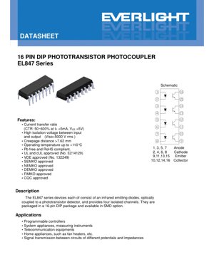
4.2 Pinout and Schematic
The pin configuration is straightforward and consistent across channels:
- Pins 1, 3, 5, 7: Anode for Channels 1-4 respectively.
- Pins 2, 4, 6, 8: Cathode for Channels 1-4 respectively.
- Pins 9, 11, 13, 15: Emitter for Channels 1-4 respectively.
- Pins 10, 12, 14, 16: Collector for Channels 1-4 respectively.
This arrangement groups all inputs on one side (pins 1-8) and all outputs on the opposite side (pins 9-16), physically reinforcing the isolation barrier.
4.3 Device Marking
Devices are marked on the top with \"EL847\" (device number), followed by a 1-digit year code (Y), a 2-digit week code (WW), and an optional \"V\" suffix denoting VDE approval for that unit.
5. Soldering & Assembly Guidelines
5.1 Reflow Soldering Profile
The datasheet provides a detailed reflow profile compliant with IPC/JEDEC J-STD-020D for lead-free soldering:
- Preheat: 150°C to 200°C over 60-120 seconds.
- Time Above Liquidus (TL=217°C): 60-100 seconds.
- Peak Temperature (TP): 260°C maximum.
- Time within 5°C of Peak: 30 seconds maximum.
- Maximum Ramp-Up Rate: 3°C/second from Tsmax to Tp.
- Maximum Ramp-Down Rate: 6°C/second.
- Total Cycle Time: 8 minutes maximum from 25°C to peak.
- Number of Reflows: The device can withstand up to 3 reflow cycles.
Adherence to this profile is critical to prevent package cracking, delamination, or damage to the internal die and wire bonds due to thermal stress.
6. Packaging & Ordering Information
The EL847 series is ordered using the part number format: EL847X-V.
- X: Lead form option. \"S\" for surface mount, blank (none) for standard DIP.
- V: Optional suffix indicating VDE safety approval is included for that specific unit.
Packing: Both variants are supplied in tubes containing 20 units each.
7. Application Suggestions
7.1 Typical Application Circuits
The EL847 is versatile and can be used in various configurations:
- Digital Signal Isolation: Connect the input LED in series with a current-limiting resistor to a microcontroller GPIO pin. The output collector can be pulled up to the isolated side's logic voltage through a resistor. The emitter is typically grounded. This provides noise-immune transmission of ON/OFF signals, such as in PLC I/O modules.
- Analog Signal Isolation (Linear Mode): By operating the phototransistor in its linear region (not saturated), the output current can be made roughly proportional to the input LED current. This requires careful biasing and is subject to CTR variations and temperature drift. It is often used for low-bandwidth, low-accuracy analog isolation.
- Driving Small Loads: The output can directly drive small loads like relays, LEDs, or optotriac drivers, provided the collector current and voltage ratings are not exceeded.
7.2 Design Considerations & Best Practices
- CTR Selection and Circuit Design: The wide CTR range (50-600%) necessitates careful design. For digital switching, choose a CTR bin that guarantees saturation of the output transistor at the minimum specified CTR with your chosen IF and load resistor (RL). The condition IC = CTRmin * IF must be greater than VCC/RL to ensure saturation.
- Speed vs. Current Trade-off: Higher IF generally improves switching speed (reduces tr/tf) but decreases CTR over time due to LED aging. A design should use the lowest IF that meets speed and noise immunity requirements.
- Noise Immunity and Bypassing: To improve common-mode transient immunity (CMTI), use a bypass capacitor (e.g., 0.1 μF) between the supply and ground on both the input and output sides, placed as close to the device pins as possible. This helps counteract the effects of the internal coupling capacitance (CIO).
- Heat Dissipation: Observe the total power dissipation limits (PTOT = 200 mW). Power is calculated as (IF * VF) on the input side plus (IC * VCE) on the output side.
8. Technical Comparison & Key Advantages
The EL847 differentiates itself in the market through several key features:
- High Isolation Voltage (5000 Vrms): Exceeds the requirements of many industrial control and power supply applications, providing a significant safety margin.
- Wide Operating Temperature Range (-55°C to +110°C): Suitable for harsh industrial and automotive environments where temperature extremes are common.
- Comprehensive Safety Approvals: UL, cUL, VDE, SEMKO, NEMKO, DEMKO, FIMKO, and CQC approvals simplify the process of incorporating the device into end products that require certification for various global markets.
- Four Channels in One Package: Offers board space savings and cost efficiency compared to using four single-channel optocouplers for multi-signal isolation tasks.
- Dual Package Options: Availability in both through-hole (DIP) and surface-mount (SMD) forms provides flexibility for both prototyping and high-volume automated assembly.
9. Frequently Asked Questions (Based on Technical Parameters)
Q1: How do I select the correct current-limiting resistor for the input LED?
A1: Use the formula: Rlimit = (Vsupply - VF) / IF. Use the maximum VF from the datasheet (1.4V) for a worst-case design to ensure IF is not exceeded. Choose IF based on required CTR and speed; 5-20 mA is typical.
Q2: My circuit isn't switching fully. The output voltage doesn't go low enough. What's wrong?
A2: The phototransistor is likely not entering saturation. This is usually a CTR issue. Verify that your design uses the minimum CTR (50%) for calculations. Increase IF or increase the value of the pull-up resistor RL on the collector to reduce the required IC for saturation (IC(sat) ≈ VCC/RL).
Q3: Can I use this for isolating analog signals like sensor outputs?
A3: It is possible but challenging. The phototransistor's linearity is poor, and CTR varies significantly with temperature and device-to-device. For accurate analog isolation, dedicated isolation amplifiers or linear optocouplers (which include feedback to compensate for nonlinearities) are strongly recommended.
Q4: What is the significance of the creepage distance >7.62 mm?
A4: Creepage is the shortest path along the surface of the insulating package between conductive parts (e.g., input pin 1 and output pin 9). A longer creepage distance prevents surface tracking (arcing across the surface due to contamination or humidity) and is a mandatory requirement for safety certifications at high isolation voltages like 5000 Vrms.
10. Practical Design Case Study
Scenario: Isolating four digital control signals from a microcontroller to a 24V industrial actuator driver.
- Requirements: Signal frequency < 1 kHz, high noise immunity, isolation for safety and ground loop prevention.
- Design Choices:
- Device: EL847 (Standard DIP).
- Input Side: Microcontroller GPIO (3.3V, capable of 20mA). Choose IF = 10 mA for good speed and longevity. Rlimit = (3.3V - 1.4V) / 0.01A = 190Ω. Use a standard 200Ω resistor.
- Output Side: Actuator driver expects a 24V logic high, pulled to ground for ON. Connect collector to 24V supply via a pull-up resistor. Choose RL to ensure saturation at minimum CTR. Required IC(sat) > 24V / RL. With CTRmin=50% and IF=10mA, IC >= 5mA. Therefore, RL must be < 24V / 0.005A = 4.8 kΩ. A 3.3 kΩ resistor is chosen, giving IC(sat) ≈ 7.3mA, which is well within the device's 50mA rating and provides a good margin.
- Bypassing: Add a 0.1 μF ceramic capacitor between Pin 10 (Collector 1) and Pin 9 (Emitter 1), and similarly for other channels, to improve noise immunity.
- Result: A robust, electrically isolated interface capable of reliably transmitting control signals in an electrically noisy industrial environment.
11. Operating Principle
A photocoupler's operation is based on electro-optical-electrical conversion. When a forward current (IF) is applied to the input Infrared Emitting Diode (IRED), it emits photons (light) with a wavelength typically around 940 nm. This light travels across a transparent insulating gap (often made of mold compound or air) within the package. The light strikes the base region of the output silicon phototransistor. The absorbed photons generate electron-hole pairs, creating a base current that turns the transistor on, allowing a collector current (IC) to flow. The key point is that the only connection between the input and output is the beam of light, providing the galvanic isolation. The ratio IC/IF is the Current Transfer Ratio (CTR), which depends on the LED's luminous efficiency, the phototransistor's sensitivity, and the optical coupling efficiency between them.
12. Industry Trends & Context
Photocouplers like the EL847 remain fundamental components in power electronics, industrial automation, and renewable energy systems where high-voltage isolation is non-negotiable. The trend in this sector is towards:
- Higher Speed: Development of digital isolators based on CMOS RF or capacitive coupling technologies offering data rates in the Mbps to Gbps range, far exceeding the ~100 kHz limit of traditional phototransistor couplers.
- Higher Integration Combining isolation with other functions like gate drivers, ADC interfaces, or USB/I2C/SPI isolators in single packages.
- Improved Reliability & Lifetime: Focus on LED technology with lower degradation over time and temperature, leading to more stable CTR over the product's lifetime.
- Miniaturization: Moving towards smaller, surface-mount packages like SOIC-8 and even smaller, while maintaining or improving isolation ratings.
Despite these trends, phototransistor-based photocouplers maintain strong relevance due to their simplicity, robustness, high isolation voltage capability, ease of use, and cost-effectiveness for applications requiring medium-to-low speed signal isolation, such as the programmable controllers, home appliances, and telecommunication equipment listed in the EL847 datasheet. Their comprehensive safety certifications make them a trusted choice for designs requiring regulatory approval.
LED Specification Terminology
Complete explanation of LED technical terms
Photoelectric Performance
| Term | Unit/Representation | Simple Explanation | Why Important |
|---|---|---|---|
| Luminous Efficacy | lm/W (lumens per watt) | Light output per watt of electricity, higher means more energy efficient. | Directly determines energy efficiency grade and electricity cost. |
| Luminous Flux | lm (lumens) | Total light emitted by source, commonly called "brightness". | Determines if the light is bright enough. |
| Viewing Angle | ° (degrees), e.g., 120° | Angle where light intensity drops to half, determines beam width. | Affects illumination range and uniformity. |
| CCT (Color Temperature) | K (Kelvin), e.g., 2700K/6500K | Warmth/coolness of light, lower values yellowish/warm, higher whitish/cool. | Determines lighting atmosphere and suitable scenarios. |
| CRI / Ra | Unitless, 0–100 | Ability to render object colors accurately, Ra≥80 is good. | Affects color authenticity, used in high-demand places like malls, museums. |
| SDCM | MacAdam ellipse steps, e.g., "5-step" | Color consistency metric, smaller steps mean more consistent color. | Ensures uniform color across same batch of LEDs. |
| Dominant Wavelength | nm (nanometers), e.g., 620nm (red) | Wavelength corresponding to color of colored LEDs. | Determines hue of red, yellow, green monochrome LEDs. |
| Spectral Distribution | Wavelength vs intensity curve | Shows intensity distribution across wavelengths. | Affects color rendering and quality. |
Electrical Parameters
| Term | Symbol | Simple Explanation | Design Considerations |
|---|---|---|---|
| Forward Voltage | Vf | Minimum voltage to turn on LED, like "starting threshold". | Driver voltage must be ≥Vf, voltages add up for series LEDs. |
| Forward Current | If | Current value for normal LED operation. | Usually constant current drive, current determines brightness & lifespan. |
| Max Pulse Current | Ifp | Peak current tolerable for short periods, used for dimming or flashing. | Pulse width & duty cycle must be strictly controlled to avoid damage. |
| Reverse Voltage | Vr | Max reverse voltage LED can withstand, beyond may cause breakdown. | Circuit must prevent reverse connection or voltage spikes. |
| Thermal Resistance | Rth (°C/W) | Resistance to heat transfer from chip to solder, lower is better. | High thermal resistance requires stronger heat dissipation. |
| ESD Immunity | V (HBM), e.g., 1000V | Ability to withstand electrostatic discharge, higher means less vulnerable. | Anti-static measures needed in production, especially for sensitive LEDs. |
Thermal Management & Reliability
| Term | Key Metric | Simple Explanation | Impact |
|---|---|---|---|
| Junction Temperature | Tj (°C) | Actual operating temperature inside LED chip. | Every 10°C reduction may double lifespan; too high causes light decay, color shift. |
| Lumen Depreciation | L70 / L80 (hours) | Time for brightness to drop to 70% or 80% of initial. | Directly defines LED "service life". |
| Lumen Maintenance | % (e.g., 70%) | Percentage of brightness retained after time. | Indicates brightness retention over long-term use. |
| Color Shift | Δu′v′ or MacAdam ellipse | Degree of color change during use. | Affects color consistency in lighting scenes. |
| Thermal Aging | Material degradation | Deterioration due to long-term high temperature. | May cause brightness drop, color change, or open-circuit failure. |
Packaging & Materials
| Term | Common Types | Simple Explanation | Features & Applications |
|---|---|---|---|
| Package Type | EMC, PPA, Ceramic | Housing material protecting chip, providing optical/thermal interface. | EMC: good heat resistance, low cost; Ceramic: better heat dissipation, longer life. |
| Chip Structure | Front, Flip Chip | Chip electrode arrangement. | Flip chip: better heat dissipation, higher efficacy, for high-power. |
| Phosphor Coating | YAG, Silicate, Nitride | Covers blue chip, converts some to yellow/red, mixes to white. | Different phosphors affect efficacy, CCT, and CRI. |
| Lens/Optics | Flat, Microlens, TIR | Optical structure on surface controlling light distribution. | Determines viewing angle and light distribution curve. |
Quality Control & Binning
| Term | Binning Content | Simple Explanation | Purpose |
|---|---|---|---|
| Luminous Flux Bin | Code e.g., 2G, 2H | Grouped by brightness, each group has min/max lumen values. | Ensures uniform brightness in same batch. |
| Voltage Bin | Code e.g., 6W, 6X | Grouped by forward voltage range. | Facilitates driver matching, improves system efficiency. |
| Color Bin | 5-step MacAdam ellipse | Grouped by color coordinates, ensuring tight range. | Guarantees color consistency, avoids uneven color within fixture. |
| CCT Bin | 2700K, 3000K etc. | Grouped by CCT, each has corresponding coordinate range. | Meets different scene CCT requirements. |
Testing & Certification
| Term | Standard/Test | Simple Explanation | Significance |
|---|---|---|---|
| LM-80 | Lumen maintenance test | Long-term lighting at constant temperature, recording brightness decay. | Used to estimate LED life (with TM-21). |
| TM-21 | Life estimation standard | Estimates life under actual conditions based on LM-80 data. | Provides scientific life prediction. |
| IESNA | Illuminating Engineering Society | Covers optical, electrical, thermal test methods. | Industry-recognized test basis. |
| RoHS / REACH | Environmental certification | Ensures no harmful substances (lead, mercury). | Market access requirement internationally. |
| ENERGY STAR / DLC | Energy efficiency certification | Energy efficiency and performance certification for lighting. | Used in government procurement, subsidy programs, enhances competitiveness. |