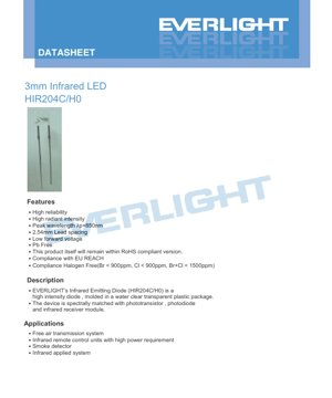
1. Product Overview
The HIR204C/H0 is a high-intensity infrared emitting diode housed in a 3.0mm water-clear transparent plastic package. It is designed for applications requiring reliable infrared emission with specific spectral characteristics.
1.1 Core Features and Advantages
The device offers several key advantages for infrared system design:
- High Reliability: Engineered for consistent performance and long operational life.
- High Radiant Intensity: Delivers strong infrared output, suitable for medium-range applications.
- Peak Wavelength: The emission is centered at a typical wavelength (λp) of 850 nanometers, which is a common standard for many IR receivers and sensors.
- Low Forward Voltage: Typically 1.45V at 20mA, contributing to lower power consumption in the driving circuit.
- Environmental Compliance: The product is Pb-Free, compliant with EU REACH regulations, and meets Halogen-Free requirements (Br < 900ppm, Cl < 900ppm, Br+Cl < 1500ppm). The product itself remains within RoHS compliant specifications.
- Standard Lead Spacing: Features a 2.54mm (0.1 inch) lead pitch, compatible with standard prototyping boards and PCB layouts.
1.2 Target Applications
This infrared LED is spectrally matched with common phototransistors, photodiodes, and infrared receiver modules, making it suitable for a variety of systems including:
- Free air transmission systems for data or signal communication.
- Infrared remote control units that require higher power output for extended range or through obstacles.
- Smoke detectors, where IR beams are used for particle detection.
- Other general infrared applied systems such as object sensing, proximity detection, and industrial automation.
2. Technical Specifications Deep Dive
2.1 Absolute Maximum Ratings
These ratings define the limits beyond which permanent damage to the device may occur. Operation under these conditions is not guaranteed.
- Continuous Forward Current (IF): 100 mA
- Peak Forward Current (IFP): 1.0 A. This rating applies under pulsed conditions with a pulse width ≤ 100μs and a duty cycle ≤ 1%.
- Reverse Voltage (VR): 5 V
- Operating Temperature (Topr): -40°C to +85°C
- Storage Temperature (Tstg): -40°C to +85°C
- Soldering Temperature (Tsol): 260°C maximum for a duration not exceeding 5 seconds.
- Power Dissipation (Pd): 150 mW at or below an ambient temperature of 25°C in free air.
2.2 Electro-Optical Characteristics
These parameters are measured at an ambient temperature (Ta) of 25°C and define the typical performance of the device.
- Radiant Intensity (Ie): A measure of the infrared power emitted per solid angle.
- Typical value is 20 mW/sr when driven at a forward current (IF) of 20mA.
- Under pulsed conditions (IF=100mA, Pulse Width ≤100μs, Duty ≤1%), the typical radiant intensity is 40 mW/sr.
- Peak Wavelength (λp): 850 nm (typical) at IF=20mA. This is the wavelength at which the emission intensity is highest.
- Spectral Bandwidth (Δλ): 45 nm (typical) at IF=20mA. This defines the range of wavelengths emitted, centered around the peak.
- Forward Voltage (VF):
- 1.45V (typical), 1.65V (maximum) at IF=20mA.
- 1.80V (typical), 2.40V (maximum) at IF=100mA under pulsed conditions.
- Reverse Current (IR): Maximum of 10 μA when a reverse voltage (VR) of 5V is applied.
- View Angle (2θ1/2): 40 degrees (typical) at IF=20mA. This is the full angle at which the radiant intensity drops to half of its maximum value (on-axis).
Measurement Tolerances: Forward Voltage: ±0.1V; Radiant Intensity: ±10%; Peak Wavelength: ±1.0nm.
3. Binning System Explanation
The HIR204C/H0 is available in different performance grades, or \"bins,\" primarily based on radiant intensity. This allows designers to select a device that meets the specific output requirements of their application.
3.1 Radiant Intensity Binning
The binning is defined at a standard test condition of IF = 20mA. The unit for radiant intensity is mW/sr.
- Bin N: Minimum 11.0, Maximum 17.6
- Bin P: Minimum 15.0, Maximum 24.0
- Bin Q: Minimum 21.0, Maximum 34.0
- Bin R: Minimum 30.0, Maximum 48.0
Selection of a higher bin (e.g., R vs. N) ensures a higher minimum guaranteed radiant output, which can translate to longer range or stronger signal strength in an application.
4. Performance Curve Analysis
The datasheet provides several characteristic curves that illustrate the device's behavior under varying conditions. Understanding these is crucial for robust circuit design.
4.1 Forward Current vs. Ambient Temperature
This curve shows the derating of the maximum allowable continuous forward current as the ambient temperature increases. At 25°C, the maximum is 100mA. As temperature rises, this maximum current must be reduced to prevent exceeding the device's power dissipation limit and causing thermal damage. The curve typically shows a linear decrease from 100mA at 25°C to a lower value at 85°C.
4.2 Spectral Distribution
This graph plots relative radiant intensity against wavelength. It visually confirms the peak wavelength (λp) of 850nm and the spectral bandwidth (Δλ) of approximately 45nm. The curve is typically Gaussian in shape, centered on 850nm.
4.3 Radiant Intensity vs. Forward Current
This is a key design curve. It shows that radiant intensity (Ie) increases with forward current (IF), but the relationship is not perfectly linear, especially at higher currents. There is a point of diminishing returns where increasing current yields less additional optical output and generates significantly more heat. Designers often operate the LED at or below the recommended continuous current (20mA or 100mA pulsed) based on this curve and thermal considerations.
4.4 Relative Radiant Intensity vs. Angular Displacement
This polar plot illustrates the spatial emission pattern of the LED. It shows how the intensity drops off as you move away from the central axis (0°). The \"view angle\" of 40° is defined where the intensity falls to 50% of its on-axis value. This information is vital for optical design, determining beam coverage, and aligning the LED with a receiver.
5. Mechanical and Package Information
5.1 Package Dimensions
The LED is housed in a standard 3.0mm round package. The detailed mechanical drawing in the datasheet provides all critical dimensions including:
- Overall diameter and height of the epoxy lens.
- Lead diameter and length.
- Distance from the base of the lens to the bend in the leads.
- The seating plane.
General Tolerance: Unless otherwise specified, dimensions have a tolerance of ±0.25mm. It is essential to refer to the exact drawing for PCB hole placement and mechanical fit.
5.2 Polarity Identification
<>The package typically uses a flat side on the rim or a longer lead to denote the cathode (negative side). The datasheet drawing will clearly indicate the anode and cathode. Correct polarity must be observed during circuit assembly.6. Soldering and Assembly Guidelines
Proper handling is critical to maintain device reliability and performance.
6.1 Lead Forming
- Bending must be done at a point at least 3mm from the base of the epoxy bulb.
- Always form leads before soldering the component.
- Avoid applying stress to the LED package or its base during forming, as this can damage internal connections or crack the epoxy.
- Cut leads at room temperature. High-temperature cutting can induce failures.
- Ensure PCB holes align perfectly with LED leads to avoid mounting stress.
6.2 Storage Conditions
- Recommended storage after receipt: ≤ 30°C and ≤ 70% Relative Humidity.
- Shelf life under these conditions is 3 months.
- For longer storage (up to 1 year), place in a sealed container with a nitrogen atmosphere and desiccant.
- Once the original packaging is opened, use components within 24 hours.
- Avoid rapid temperature changes in humid environments to prevent condensation.
6.3 Soldering Recommendations
The solder joint must be at least 3mm away from the epoxy bulb.
- Hand Soldering: Iron tip temperature ≤ 300°C (for a 30W max iron). Soldering time ≤ 3 seconds per lead.
- Wave/Dip Soldering: Preheat temperature ≤ 100°C for ≤ 60 seconds. Solder bath temperature ≤ 260°C for ≤ 5 seconds.
- General Rules:
- Avoid stress on leads during and immediately after soldering while the device is hot.
- Do not perform dip/hand soldering more than once.
- Protect the LED from mechanical shock/vibration until it cools to room temperature after soldering.
- Avoid rapid cooling processes.
- Always use the lowest effective soldering temperature and time.
6.4 Cleaning
- If cleaning is necessary, use isopropyl alcohol at room temperature for no more than one minute. Air dry at room temperature.
- Avoid ultrasonic cleaning. If absolutely required, extensive pre-qualification is necessary to ensure the specific ultrasonic power and assembly conditions do not damage the LED die or wire bonds.
6.5 Thermal Management
Although not detailed with specific thermal resistance values in this datasheet, heat management is emphasized. The power dissipation (Pd) rating of 150mW is for free air at 25°C. In real applications, especially when driving at higher currents or in enclosed spaces, the LED's junction temperature will rise. This can reduce luminous efficacy and lifespan. Designers must consider heat sinking, PCB copper area, and ambient conditions during the application design phase to ensure the LED operates within safe temperature limits.
7. Packaging and Ordering Information
7.1 Label Specification
The label on the packaging contains key information for traceability and identification:
- CPN: Customer's Product Number
- P/N: Product Number (e.g., HIR204C/H0)
- QTY: Quantity in the package
- CAT: Luminous Intensity Rank (Bin code, e.g., N, P, Q, R)
- HUE: Dominant Wavelength Rank
- REF: Forward Voltage Rank
- LOT No: Manufacturing Lot Number
- X: Month of production
- REF: Label reference number
7.2 Packing Specification
- Primary Packaging: Anti-static bags.
- Secondary Packaging: Inner cartons.
- Tertiary Packaging: Master outside cartons.
- Standard Packing Quantity:
- 200 to 1000 pieces per anti-static bag.
- 5 bags are packed into 1 inner carton.
- 10 inner cartons are packed into 1 outside carton.
8. Application Design Considerations
8.1 Driving Circuit Design
To operate the LED, a current-limiting circuit is mandatory. A simple series resistor is often sufficient for basic applications. The resistor value (R) can be calculated using Ohm's Law: R = (Vsupply - Vf) / If. For example, with a 5V supply, a Vf of 1.45V, and a desired If of 20mA: R = (5 - 1.45) / 0.02 = 177.5Ω. A standard 180Ω resistor would be suitable. For pulsed operation at higher currents (e.g., 100mA), a transistor or dedicated LED driver IC is recommended to provide the necessary current pulse.
8.2 Optical Design and Alignment
The 40-degree viewing angle provides a reasonably broad beam. For longer-range or focused applications, a lens may be added in front of the LED. Conversely, for very wide coverage, multiple LEDs may be needed. Precise mechanical alignment with the receiving sensor (phototransistor, IR receiver module) is crucial for optimal system performance. The spatial emission pattern curve should be consulted to understand signal strength at off-axis angles.
8.3 Interference and Noise Immunity
Infrared systems can be susceptible to ambient light noise, particularly from sunlight and incandescent lamps which contain IR components. Strategies to mitigate this include:
- Using modulated IR signals (e.g., 38kHz carrier) and a receiver tuned to the same frequency.
- Adding an optical filter that blocks visible light but passes 850nm IR on the receiver side.
- Physically shielding the LED and receiver pair from direct ambient light sources.
9. Technical Comparison and Positioning
The HIR204C/H0 occupies a specific position in the infrared LED market. Compared to smaller SMD IR LEDs, it offers higher potential radiant output due to its larger die size and package, making it suitable for applications needing more power. Compared to larger, dedicated high-power IR emitters, it is more compact and easier to drive with simple circuits. Its 850nm wavelength is the most common, ensuring broad compatibility with receivers. Key differentiators include its clear package (no tint), standard 2.54mm lead spacing for easy prototyping, and well-defined binning structure for output consistency.
10. Frequently Asked Questions (Based on Technical Parameters)
10.1 What is the difference between Continuous Current (IF) and Peak Current (IFP)?
Continuous Forward Current (IF=100mA) is the maximum DC current that can be passed through the LED indefinitely without causing damage, assuming thermal limits are respected. Peak Forward Current (IFP=1.0A) is the maximum current allowed only under very short pulse conditions (≤100μs pulse width, ≤1% duty cycle). This allows for brief, high-intensity bursts of light for applications like long-range remote controls, but the average power must remain within the device's dissipation limits.
10.2 How do I select the correct Bin (N, P, Q, R)?
Choose based on the minimum radiant intensity your application requires at the operating distance and under worst-case conditions (e.g., low battery, high temperature). If your design calculations show you need at least 18 mW/sr, you must select Bin Q (Min 21.0) or Bin R (Min 30.0). Bin N (Min 11.0) would not be guaranteed to work. Selecting a higher bin provides more design margin.
10.3 Why is the soldering distance (3mm from the bulb) so important?
The epoxy resin that forms the lens has a different coefficient of thermal expansion than the metal leads. Applying high soldering heat too close to the epoxy can cause thermal stress, potentially leading to micro-cracks in the epoxy or damage to the internal die attach. These cracks can allow moisture ingress later, leading to premature failure. The 3mm distance allows the heat to dissipate along the lead before reaching the sensitive package.
11. Design and Usage Case Study
11.1 Case: Improving Range of a Consumer IR Remote Control
Scenario: A designer is creating a universal remote control that needs to work reliably from up to 10 meters away, even at slight angles, in a typical living room.
Design Choices using HIR204C/H0:
- Drive Current: Instead of using the typical 20mA continuous, the designer uses a pulsed drive circuit. They pulse the LED at 100mA with a very short duty cycle (e.g., 0.5%) to generate high-intensity bursts, leveraging the IFP rating. This significantly boosts the peak optical power and thus the effective range.
- Bin Selection: To ensure consistent performance across all manufactured units and account for battery voltage drop, the designer specifies Bin R LEDs. This guarantees a high minimum output even at the end of the battery's life.
- Placement and Lens: Two LEDs are placed slightly apart and angled a few degrees from each other to create a wider effective beam pattern, improving the chance of hitting the receiver from various angles. A simple, low-cost plastic lens cap is used over the LEDs to collimate the beam slightly for better directionality.
- Thermal Consideration: Since the duty cycle is very low (0.5%), the average power is small (100mA * 1.65V * 0.005 = 0.825mW), well below the 150mW Pd rating. No special heat sinking is required on the PCB.
This approach demonstrates how understanding the datasheet's pulsed ratings, binning, and thermal parameters enables an optimized, cost-effective design for a demanding application.
12. Operating Principle
An Infrared Light Emitting Diode (IR LED) operates on the same fundamental principle as a standard visible LED but uses different semiconductor materials to produce light in the infrared spectrum. The HIR204C/H0 uses a Gallium Aluminum Arsenide (GaAlAs) chip. When a forward voltage is applied across the LED's P-N junction, electrons and holes recombine in the active region of the semiconductor. This recombination process releases energy in the form of photons. The specific bandgap energy of the GaAlAs material determines the wavelength of these photons, which in this case is centered around 850 nanometers, placing it in the near-infrared region, invisible to the human eye. The water-clear epoxy package does not filter or tint the light, allowing the maximum amount of the generated infrared radiation to escape.
13. Technology Trends
The field of infrared emitters continues to evolve. General trends observable in the industry include:
- Increased Efficiency: Development of new semiconductor epitaxial structures to achieve higher radiant intensity (mW/sr) for the same input current (mA), improving overall system power efficiency.
- Miniaturization: While through-hole packages like the 3mm remain popular for robustness and ease of use, there is a strong trend towards surface-mount device (SMD) packages (e.g., 0805, 0603) for automated assembly and space-constrained designs like smartphones (for proximity sensors) and tiny IoT devices.
- Wavelength Diversification: While 850nm and 940nm are dominant, there is growing use of other wavelengths for specific applications, such as 810nm for medical devices or specific narrow bands for gas sensing.
- Integration: Combining the IR LED with a driver circuit, modulator, or even a photodetector in a single package to create smarter, easier-to-use \"sensor modules.\"
- Enhanced Reliability Data: Modern datasheets are increasingly providing more detailed lifetime and reliability data (e.g., L70, L50 figures under various stress conditions) to support designs for automotive, industrial, and medical applications where long-term performance is critical.
The HIR204C/H0 represents a mature, reliable, and well-understood component that benefits from these ongoing material and manufacturing advancements, ensuring its continued relevance in a wide array of electronic designs.
LED Specification Terminology
Complete explanation of LED technical terms
Photoelectric Performance
| Term | Unit/Representation | Simple Explanation | Why Important |
|---|---|---|---|
| Luminous Efficacy | lm/W (lumens per watt) | Light output per watt of electricity, higher means more energy efficient. | Directly determines energy efficiency grade and electricity cost. |
| Luminous Flux | lm (lumens) | Total light emitted by source, commonly called "brightness". | Determines if the light is bright enough. |
| Viewing Angle | ° (degrees), e.g., 120° | Angle where light intensity drops to half, determines beam width. | Affects illumination range and uniformity. |
| CCT (Color Temperature) | K (Kelvin), e.g., 2700K/6500K | Warmth/coolness of light, lower values yellowish/warm, higher whitish/cool. | Determines lighting atmosphere and suitable scenarios. |
| CRI / Ra | Unitless, 0–100 | Ability to render object colors accurately, Ra≥80 is good. | Affects color authenticity, used in high-demand places like malls, museums. |
| SDCM | MacAdam ellipse steps, e.g., "5-step" | Color consistency metric, smaller steps mean more consistent color. | Ensures uniform color across same batch of LEDs. |
| Dominant Wavelength | nm (nanometers), e.g., 620nm (red) | Wavelength corresponding to color of colored LEDs. | Determines hue of red, yellow, green monochrome LEDs. |
| Spectral Distribution | Wavelength vs intensity curve | Shows intensity distribution across wavelengths. | Affects color rendering and quality. |
Electrical Parameters
| Term | Symbol | Simple Explanation | Design Considerations |
|---|---|---|---|
| Forward Voltage | Vf | Minimum voltage to turn on LED, like "starting threshold". | Driver voltage must be ≥Vf, voltages add up for series LEDs. |
| Forward Current | If | Current value for normal LED operation. | Usually constant current drive, current determines brightness & lifespan. |
| Max Pulse Current | Ifp | Peak current tolerable for short periods, used for dimming or flashing. | Pulse width & duty cycle must be strictly controlled to avoid damage. |
| Reverse Voltage | Vr | Max reverse voltage LED can withstand, beyond may cause breakdown. | Circuit must prevent reverse connection or voltage spikes. |
| Thermal Resistance | Rth (°C/W) | Resistance to heat transfer from chip to solder, lower is better. | High thermal resistance requires stronger heat dissipation. |
| ESD Immunity | V (HBM), e.g., 1000V | Ability to withstand electrostatic discharge, higher means less vulnerable. | Anti-static measures needed in production, especially for sensitive LEDs. |
Thermal Management & Reliability
| Term | Key Metric | Simple Explanation | Impact |
|---|---|---|---|
| Junction Temperature | Tj (°C) | Actual operating temperature inside LED chip. | Every 10°C reduction may double lifespan; too high causes light decay, color shift. |
| Lumen Depreciation | L70 / L80 (hours) | Time for brightness to drop to 70% or 80% of initial. | Directly defines LED "service life". |
| Lumen Maintenance | % (e.g., 70%) | Percentage of brightness retained after time. | Indicates brightness retention over long-term use. |
| Color Shift | Δu′v′ or MacAdam ellipse | Degree of color change during use. | Affects color consistency in lighting scenes. |
| Thermal Aging | Material degradation | Deterioration due to long-term high temperature. | May cause brightness drop, color change, or open-circuit failure. |
Packaging & Materials
| Term | Common Types | Simple Explanation | Features & Applications |
|---|---|---|---|
| Package Type | EMC, PPA, Ceramic | Housing material protecting chip, providing optical/thermal interface. | EMC: good heat resistance, low cost; Ceramic: better heat dissipation, longer life. |
| Chip Structure | Front, Flip Chip | Chip electrode arrangement. | Flip chip: better heat dissipation, higher efficacy, for high-power. |
| Phosphor Coating | YAG, Silicate, Nitride | Covers blue chip, converts some to yellow/red, mixes to white. | Different phosphors affect efficacy, CCT, and CRI. |
| Lens/Optics | Flat, Microlens, TIR | Optical structure on surface controlling light distribution. | Determines viewing angle and light distribution curve. |
Quality Control & Binning
| Term | Binning Content | Simple Explanation | Purpose |
|---|---|---|---|
| Luminous Flux Bin | Code e.g., 2G, 2H | Grouped by brightness, each group has min/max lumen values. | Ensures uniform brightness in same batch. |
| Voltage Bin | Code e.g., 6W, 6X | Grouped by forward voltage range. | Facilitates driver matching, improves system efficiency. |
| Color Bin | 5-step MacAdam ellipse | Grouped by color coordinates, ensuring tight range. | Guarantees color consistency, avoids uneven color within fixture. |
| CCT Bin | 2700K, 3000K etc. | Grouped by CCT, each has corresponding coordinate range. | Meets different scene CCT requirements. |
Testing & Certification
| Term | Standard/Test | Simple Explanation | Significance |
|---|---|---|---|
| LM-80 | Lumen maintenance test | Long-term lighting at constant temperature, recording brightness decay. | Used to estimate LED life (with TM-21). |
| TM-21 | Life estimation standard | Estimates life under actual conditions based on LM-80 data. | Provides scientific life prediction. |
| IESNA | Illuminating Engineering Society | Covers optical, electrical, thermal test methods. | Industry-recognized test basis. |
| RoHS / REACH | Environmental certification | Ensures no harmful substances (lead, mercury). | Market access requirement internationally. |
| ENERGY STAR / DLC | Energy efficiency certification | Energy efficiency and performance certification for lighting. | Used in government procurement, subsidy programs, enhances competitiveness. |