Table of Contents
- 1. Product Overview
- 2. Technical Specifications Deep Dive
- 2.1 Absolute Maximum Ratings
- 2.2 Electro-Optical Characteristics
- 3. Performance Curve Analysis
- 4. Mechanical & Package Information
- 4.1 Pin Configuration
- 4.2 Package Dimension Drawings
- 5. Soldering & Assembly Guidelines
- 6. Ordering Information & Packaging
- 6.1 Part Numbering System
- 6.2 Packaging Quantities
- 6.3 Device Marking
- 7. Application Suggestions
- 7.1 Typical Application Circuits
- 7.2 Design Considerations & Best Practices
- 8. Technical Comparison & Differentiation
- 9. Frequently Asked Questions (FAQ)
1. Product Overview
The EL817-G series represents a family of phototransistor-based photocouplers (optocouplers) designed for signal isolation and transmission between circuits of different potentials. Each device integrates an infrared emitting diode optically coupled to a silicon phototransistor detector, housed within a compact 4-pin Dual In-line Package (DIP). The primary function is to provide electrical isolation, preventing voltage spikes, ground loops, and noise from propagating between input and output circuits, thereby protecting sensitive components and ensuring signal integrity.
The core value proposition of this series lies in its robust isolation capabilities, verified by a high isolation voltage rating of 5000Vrms. This makes it suitable for industrial control systems and mains-connected appliances. The devices are manufactured to be halogen-free, complying with environmental regulations (Br < 900 ppm, Cl < 900 ppm, Br+Cl < 1500 ppm). They also carry approvals from major international safety standards bodies including UL, cUL, VDE, SEMKO, NEMKO, DEMKO, FIMKO, and CQC, underscoring their reliability for use in certified end products.
2. Technical Specifications Deep Dive
2.1 Absolute Maximum Ratings
These ratings define the stress limits beyond which permanent damage to the device may occur. Operation under these conditions is not guaranteed.
- Input (LED Side): The infrared diode has a maximum continuous forward current (IF) of 60 mA. It can withstand a very short 1 μs pulse current (IFP) of up to 1 A, useful for transient suppression. The maximum reverse voltage (VR) is 6 V. Input power dissipation (PD) is rated at 100 mW at 25°C, derating by 2.9 mW/°C above 100°C ambient temperature.
- Output (Transistor Side): The phototransistor collector current (IC) is limited to 50 mA. The collector-emitter voltage (VCEO) can be as high as 80 V, while the emitter-collector voltage (VECO) is limited to 7 V. Output power dissipation (PC) is 150 mW at 25°C, derating by 5.8 mW/°C above 100°C.
- Device Total: The total power dissipation for the entire package (PTOT) must not exceed 200 mW.
- Isolation & Environment: The isolation voltage (VISO) between input and output is 5000 Vrms (tested for 1 minute at 40-60% RH). The operating temperature range (TOPR) is exceptionally wide, from -55°C to +110°C. The storage temperature (TSTG) range is -55°C to +125°C. The device can survive soldering at 260°C for up to 10 seconds.
2.2 Electro-Optical Characteristics
These parameters define the device's performance under normal operating conditions (Ta = 25°C unless noted).
- Input Diode Characteristics: The forward voltage (VF) is typically 1.2V with a maximum of 1.4V at IF = 20 mA. Reverse current (IR) is a maximum of 10 μA at VR = 4V. Input capacitance (Cin) is typically 30 pF.
- Output Transistor Characteristics: The collector-emitter dark current (ICEO), which is the leakage current when the LED is off, is a maximum of 100 nA at VCE = 20V. Breakdown voltages are BVCEO ≥ 80V and BVECO ≥ 7V.
- Transfer Characteristics (Critical):
- Current Transfer Ratio (CTR): This is the ratio of output collector current (IC) to input LED forward current (IF), expressed as a percentage. It is the key parameter defining the device's sensitivity and gain. The EL817-G series is offered in multiple CTR grades, measured at IF = 5mA and VCE = 5V:
- EL817: 50% to 600% (broad range)
- EL817A: 80% to 160%
- EL817B: 130% to 260%
- EL817C: 200% to 400%
- EL817D: 300% to 600%
- EL817X: 100% to 200%
- EL817Y: 150% to 300%
- Saturation Voltage: The collector-emitter saturation voltage (VCE(sat)) is typically 0.1V (max 0.2V) when the device is fully on (IF=20mA, IC=1mA), indicating good switching performance.
- Isolation Parameters: The isolation resistance (RIO) is a minimum of 5×10¹⁰ Ω. The isolation capacitance (CIO) is typically 0.6 pF, which is very low and helps maintain high-frequency noise rejection.
- Switching Speed: The rise time (tr) and fall time (tf) are typically 6 μs and 8 μs, respectively (max 18 μs each), under specified test conditions (VCE=2V, IC=2mA, RL=100Ω). The cut-off frequency (fc) is typically 80 kHz. These parameters define the maximum digital signal frequency the coupler can handle effectively.
- Current Transfer Ratio (CTR): This is the ratio of output collector current (IC) to input LED forward current (IF), expressed as a percentage. It is the key parameter defining the device's sensitivity and gain. The EL817-G series is offered in multiple CTR grades, measured at IF = 5mA and VCE = 5V:
3. Performance Curve Analysis
While the PDF indicates the presence of "Typical Electro-Optical Characteristics Curves," the specific graphs are not provided in the text content. Typically, such datasheets include curves illustrating the following relationships, which are crucial for design:
- CTR vs. Forward Current (IF): Shows how the current transfer ratio changes with the driving current of the LED. CTR often decreases at very high IF due to heating and efficiency droop.
- CTR vs. Ambient Temperature (Ta): Illustrates the temperature dependence of the device's gain. Phototransistor-based couplers typically exhibit a negative temperature coefficient for CTR; gain decreases as temperature increases.
- Forward Voltage (VF) vs. Forward Current (IF): The standard diode I-V curve, important for calculating the required current-limiting resistor for the input side.
- Collector Current (IC) vs. Collector-Emitter Voltage (VCE): The output transistor's characteristic curves, showing the saturation region and the active region for different levels of input LED current (IF).
- Switching Time vs. Load Resistance (RL): Demonstrates how the choice of pull-up resistor on the collector affects the rise and fall times of the output signal.
Designers should consult the full PDF with graphs to accurately model device behavior across their intended operating conditions.
4. Mechanical & Package Information
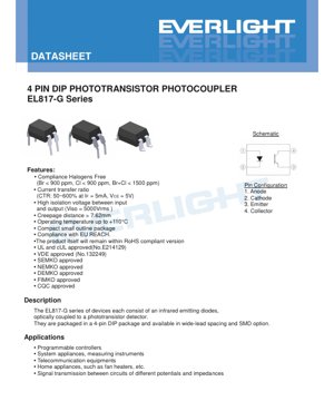
4.1 Pin Configuration
The standard 4-pin DIP pinout is as follows (viewed from the top, with the notch or dot indicating pin 1):
- Anode (of the input LED)
- Cathode (of the input LED)
- Emitter (of the output phototransistor)
- Collector (of the output phototransistor)
This configuration is consistent across the series. The creepage distance (the shortest distance along the surface of the insulating package between conductive pins) is specified as greater than 7.62 mm, which contributes to the high isolation rating.
4.2 Package Dimension Drawings
The series is offered in several package variants, though detailed dimensions in mm are not fully specified in the provided text. The options include:
- Standard DIP Type: The classic through-hole package.
- Option M Type: Features a "wide lead bend" providing a 0.4-inch (approx. 10.16 mm) lead spacing instead of the standard 0.3-inch (7.62 mm), useful for breadboarding or specific PCB layouts requiring more clearance.
- Option S1 & S2 Types: Surface-mount device (SMD) lead forms. These are "low profile" packages designed for reflow soldering. The datasheet includes recommended pad layouts for both S1 and S2 options to ensure proper soldering and mechanical stability. The pad dimensions are suggested as a reference and should be modified based on the specific PCB manufacturing process.
5. Soldering & Assembly Guidelines
The device is rated for a maximum soldering temperature (TSOL) of 260°C for 10 seconds. This aligns with common lead-free reflow soldering profiles.
For Through-Hole (DIP, M) Packages: Standard wave soldering or hand soldering techniques can be used. Care should be taken not to exceed the 10-second limit at the pin junction to prevent thermal damage to the internal die and epoxy package.
For Surface Mount (S1, S2) Packages: Standard infrared or convection reflow soldering processes are applicable. The recommended pad layout provided in the datasheet should be followed to achieve proper solder fillets and avoid tombstoning. The low-profile design aids in stability during the reflow process. As with all moisture-sensitive devices, if the reel has been exposed to ambient humidity for extended periods, baking according to IPC/JEDEC standards may be required before reflow to prevent "popcorning."
Storage: Devices should be stored within the specified storage temperature range of -55°C to +125°C, in a dry environment to maintain solderability and prevent internal corrosion.
6. Ordering Information & Packaging
6.1 Part Numbering System
The part number follows the format: EL817X(Y)(Z)-FVG
- X: Lead form option. S1 or S2 (SMD), M (Wide lead DIP), or none (Standard DIP).
- Y: CTR Rank. A, B, C, D, X, Y, or none (for the base EL817 broad range).
- Z: Tape and reel option for SMD parts. TU or TD (tape direction), or none.
- F: Lead frame material. F for Iron, none for Copper.
- V: Optional VDE safety approval marking.
- G: Denotes Halogen-free construction.
Example: EL817B-S1(TU)-G would be an SMD device (S1) with CTR rank B (130-260%), packaged in a TU-style tape and reel, with halogen-free construction.
6.2 Packaging Quantities
- Standard DIP and M options: 100 units per tube.
- S1 option on tape & reel: 1500 units per reel.
- S2 option on tape & reel: 2000 units per reel.
6.3 Device Marking
The top of the package is marked with a code: EL 817FRYWWV
- EL: Manufacturer identifier.
- 817: Device number.
- F: Factory/Process code.
- R: CTR Rank (A, B, C, D, X, Y).
- Y: 1-digit year code.
- WW: 2-digit week code.
- V: Denotes VDE approval if present.
7. Application Suggestions
7.1 Typical Application Circuits
The EL817-G is versatile and can be used in both digital and linear applications.
- Digital Signal Isolation: The most common use. The input LED is driven by a digital signal (often through a current-limiting resistor). The phototransistor acts as a switch, pulling the output line to ground when the LED is on. A pull-up resistor to VCC on the collector is required. The switching speed (tr, tf) limits the maximum data rate, making it suitable for lower-speed digital interfaces like GPIO isolation, UART, or I/O lines in PLCs.
- Analog Signal Isolation (Linear Mode): By operating the phototransistor in its active region (not saturated), the device can transmit analog signals. The CTR is not perfectly linear, and its variation with temperature and current must be accounted for. This mode is often used for isolated feedback in switch-mode power supplies, where the non-linearity can be compensated within the control loop.
- Input/Output (I/O) Module Isolation: In Programmable Logic Controllers (PLCs) and industrial control systems, these couplers isolate the sensitive CPU from noisy or high-voltage field signals (24V, 120VAC, etc.).
7.2 Design Considerations & Best Practices
- CTR Selection: Choose a CTR grade that provides sufficient output current for your load (e.g., to drive a logic gate or an opto-triac driver) without requiring excessive input current. Using a device with higher CTR allows for lower IF, reducing power consumption on the input side. However, ensure the chosen grade's minimum CTR meets the circuit's worst-case (e.g., high temperature, end-of-life) requirements.
- Input Current Limiting: Always use a series resistor (Rin) with the input LED to set the desired forward current (IF). Calculate Rin = (Vsource - VF) / IF. Do not exceed the absolute maximum IF of 60 mA continuously.
- Output Load Resistor: The value of the pull-up resistor (RL) on the collector affects both the output logic high level and the switching speed. A smaller RL provides faster fall times (transistor turning on pulls down faster) but slower rise times (the RC time constant with the transistor's output capacitance is larger) and consumes more power when the output is low. A larger RL does the opposite. A typical value is between 1kΩ and 10kΩ.
- Noise Immunity: For digital applications, adding a small capacitor (e.g., 1-10 nF) between the collector and emitter (output side) can help filter high-frequency noise. However, this will further degrade switching speed.
- Temperature Effects: Remember that CTR degrades with increasing temperature. Design must be verified over the full operating temperature range, using the minimum expected CTR at the maximum operating temperature.
- Isolation Layout: On the PCB, maintain the recommended creepage and clearance distances (≥7.62mm) between the input and output circuits. This often means leaving a slot or gap in the PCB under the coupler body and ensuring no copper traces bridge the isolation barrier too closely.
8. Technical Comparison & Differentiation
The EL817-G series competes in a crowded market of general-purpose 4-pin photocouplers. Its key differentiators are:
- High Temperature Rating: An operating temperature up to +110°C exceeds the common +85°C or +100°C ratings of many competitors, making it suitable for harsh environments like under-the-hood automotive applications or industrial equipment near heat sources.
- Multiple Safety Approvals: The comprehensive set of international safety approvals (UL, VDE, etc.) is a significant advantage for products requiring global market certification.
- Halogen-Free Compliance: Meets modern environmental regulations, which is increasingly a requirement in consumer electronics and other sectors.
- Wide CTR Grading: The availability of seven distinct CTR grades (including the broad EL817) provides designers with fine-grained control over gain selection for optimized circuit performance and cost.
- Package Variety: Offering standard DIP, wide-lead DIP, and two SMD profiles provides flexibility for different assembly processes and board space constraints.
9. Frequently Asked Questions (FAQ)
Q1: What is the main purpose of the creepage distance specification (>7.62 mm)?
A1: Creepage distance is the shortest path along the surface of the insulating package between two conductive terminals (e.g., pin 1 and pin 4). A longer creepage distance prevents surface leakage currents and arcing, especially in humid or contaminated environments, and is a critical factor in achieving the high 5000Vrms isolation rating.
Q2: How do I choose between the different CTR grades (A, B, C, D, X, Y)?
A2: Select based on your required output current and desired input current efficiency. For a given output current need, a higher CTR grade (e.g., D: 300-600%) requires a lower input LED current, saving power. However, higher CTR devices may have slightly different temperature coefficients or cost more. Grade X and Y offer intermediate, tighter ranges. Use the minimum CTR value from the datasheet for your worst-case design calculations.
Q3: Can I use this for isolating 240VAC mains signals?
A3: The 5000Vrms isolation voltage is suitable for providing reinforced insulation in many mains-connected applications. However, the final design must consider system-level safety standards (e.g., IEC 62368-1, IEC 60747-5-5), which dictate required distances and tests beyond the component rating. The coupler is a key part of the solution, but proper PCB layout and enclosure design are equally critical.
Q4: Why are there two different collector-emitter voltage ratings (VCEO 80V and BVCEO 80V)?
A4: VCEO (80V) in the Absolute Maximum Ratings table is the maximum voltage that can be applied without causing damage. BVCEO (80V min) in the Characteristics table is the breakdown voltage, the point at which the device begins to conduct significantly even with the LED off. They are closely related but defined differently. In practice, you should design so that VCE never approaches 80V during operation, leaving a safety margin.
Q5: What is the difference between the S1 and S2 SMD options?
A5: The primary difference is the package footprint and the number of units per reel (1500 for S1, 2000 for S2). The S2 package is likely slightly modified to allow more devices on a standard reel. The datasheet provides separate recommended pad layouts for each, so it is essential to use the correct footprint for the ordered part.
LED Specification Terminology
Complete explanation of LED technical terms
Photoelectric Performance
| Term | Unit/Representation | Simple Explanation | Why Important |
|---|---|---|---|
| Luminous Efficacy | lm/W (lumens per watt) | Light output per watt of electricity, higher means more energy efficient. | Directly determines energy efficiency grade and electricity cost. |
| Luminous Flux | lm (lumens) | Total light emitted by source, commonly called "brightness". | Determines if the light is bright enough. |
| Viewing Angle | ° (degrees), e.g., 120° | Angle where light intensity drops to half, determines beam width. | Affects illumination range and uniformity. |
| CCT (Color Temperature) | K (Kelvin), e.g., 2700K/6500K | Warmth/coolness of light, lower values yellowish/warm, higher whitish/cool. | Determines lighting atmosphere and suitable scenarios. |
| CRI / Ra | Unitless, 0–100 | Ability to render object colors accurately, Ra≥80 is good. | Affects color authenticity, used in high-demand places like malls, museums. |
| SDCM | MacAdam ellipse steps, e.g., "5-step" | Color consistency metric, smaller steps mean more consistent color. | Ensures uniform color across same batch of LEDs. |
| Dominant Wavelength | nm (nanometers), e.g., 620nm (red) | Wavelength corresponding to color of colored LEDs. | Determines hue of red, yellow, green monochrome LEDs. |
| Spectral Distribution | Wavelength vs intensity curve | Shows intensity distribution across wavelengths. | Affects color rendering and quality. |
Electrical Parameters
| Term | Symbol | Simple Explanation | Design Considerations |
|---|---|---|---|
| Forward Voltage | Vf | Minimum voltage to turn on LED, like "starting threshold". | Driver voltage must be ≥Vf, voltages add up for series LEDs. |
| Forward Current | If | Current value for normal LED operation. | Usually constant current drive, current determines brightness & lifespan. |
| Max Pulse Current | Ifp | Peak current tolerable for short periods, used for dimming or flashing. | Pulse width & duty cycle must be strictly controlled to avoid damage. |
| Reverse Voltage | Vr | Max reverse voltage LED can withstand, beyond may cause breakdown. | Circuit must prevent reverse connection or voltage spikes. |
| Thermal Resistance | Rth (°C/W) | Resistance to heat transfer from chip to solder, lower is better. | High thermal resistance requires stronger heat dissipation. |
| ESD Immunity | V (HBM), e.g., 1000V | Ability to withstand electrostatic discharge, higher means less vulnerable. | Anti-static measures needed in production, especially for sensitive LEDs. |
Thermal Management & Reliability
| Term | Key Metric | Simple Explanation | Impact |
|---|---|---|---|
| Junction Temperature | Tj (°C) | Actual operating temperature inside LED chip. | Every 10°C reduction may double lifespan; too high causes light decay, color shift. |
| Lumen Depreciation | L70 / L80 (hours) | Time for brightness to drop to 70% or 80% of initial. | Directly defines LED "service life". |
| Lumen Maintenance | % (e.g., 70%) | Percentage of brightness retained after time. | Indicates brightness retention over long-term use. |
| Color Shift | Δu′v′ or MacAdam ellipse | Degree of color change during use. | Affects color consistency in lighting scenes. |
| Thermal Aging | Material degradation | Deterioration due to long-term high temperature. | May cause brightness drop, color change, or open-circuit failure. |
Packaging & Materials
| Term | Common Types | Simple Explanation | Features & Applications |
|---|---|---|---|
| Package Type | EMC, PPA, Ceramic | Housing material protecting chip, providing optical/thermal interface. | EMC: good heat resistance, low cost; Ceramic: better heat dissipation, longer life. |
| Chip Structure | Front, Flip Chip | Chip electrode arrangement. | Flip chip: better heat dissipation, higher efficacy, for high-power. |
| Phosphor Coating | YAG, Silicate, Nitride | Covers blue chip, converts some to yellow/red, mixes to white. | Different phosphors affect efficacy, CCT, and CRI. |
| Lens/Optics | Flat, Microlens, TIR | Optical structure on surface controlling light distribution. | Determines viewing angle and light distribution curve. |
Quality Control & Binning
| Term | Binning Content | Simple Explanation | Purpose |
|---|---|---|---|
| Luminous Flux Bin | Code e.g., 2G, 2H | Grouped by brightness, each group has min/max lumen values. | Ensures uniform brightness in same batch. |
| Voltage Bin | Code e.g., 6W, 6X | Grouped by forward voltage range. | Facilitates driver matching, improves system efficiency. |
| Color Bin | 5-step MacAdam ellipse | Grouped by color coordinates, ensuring tight range. | Guarantees color consistency, avoids uneven color within fixture. |
| CCT Bin | 2700K, 3000K etc. | Grouped by CCT, each has corresponding coordinate range. | Meets different scene CCT requirements. |
Testing & Certification
| Term | Standard/Test | Simple Explanation | Significance |
|---|---|---|---|
| LM-80 | Lumen maintenance test | Long-term lighting at constant temperature, recording brightness decay. | Used to estimate LED life (with TM-21). |
| TM-21 | Life estimation standard | Estimates life under actual conditions based on LM-80 data. | Provides scientific life prediction. |
| IESNA | Illuminating Engineering Society | Covers optical, electrical, thermal test methods. | Industry-recognized test basis. |
| RoHS / REACH | Environmental certification | Ensures no harmful substances (lead, mercury). | Market access requirement internationally. |
| ENERGY STAR / DLC | Energy efficiency certification | Energy efficiency and performance certification for lighting. | Used in government procurement, subsidy programs, enhances competitiveness. |