Table of Contents
- 1. Product Overview
- 1.1 Core Advantages
- 1.2 Target Applications
- 2. Technical Parameter Analysis
- 2.1 Absolute Maximum Ratings
- 2.2 Electro-Optical Characteristics
- 3. Performance Curve Analysis
- 4. Mechanical & Package Information
- 4.1 Package Dimensions and Types
- 4.2 Polarity Identification and Marking
- 4.3 Recommended SMD Pad Layout
- 5. Soldering & Assembly Guidelines
- 6. Packaging & Ordering Information
- 6.1 Model Numbering System
- 6.2 Packing Specifications
- 7. Application Design Considerations
- 7.1 Input Circuit Design
- 7.2 Output Circuit Design
- 7.3 Thermal Management
- 8. Technical Comparison & Selection Guide
- 9. Frequently Asked Questions (FAQ)
- 10. Design-in Case Study Example
- 11. Operating Principle
- 12. Technology Trends
1. Product Overview
The EL4XXA-G series are single-pole, normally-open (Form A) solid-state relays (SSRs) in a 4-pin DIP package. These devices utilize an AlGaAs infrared LED optically coupled to a high-voltage output detector circuit consisting of a photovoltaic diode array and MOSFETs. This design provides a solid-state equivalent to a 1 Form A electromechanical relay (EMR), offering benefits such as longer life, silent operation, and resistance to mechanical shock and vibration. The series is available in surface-mount (SMD) options and is compliant with halogen-free and RoHS standards.
1.1 Core Advantages
- High Isolation: Provides 5000 Vrms of isolation between input and output, enhancing safety and noise immunity in control circuits.
- Low Drive Current: Features a low LED turn-on current (typically 3-5mA), making it compatible with low-power microcontroller outputs.
- Wide Voltage Range: The series covers output withstand voltages from 60V (EL406A) to 600V (EL460A), suitable for various AC/DC load switching applications.
- Robust Compliance: Halogen-free construction and compliance with major international safety standards including UL 1577, UL 508, VDE, and CQC.
- Wide Temperature Range: Operates reliably from -40°C to +85°C, suitable for industrial and harsh environments.
1.2 Target Applications
These SSRs are designed for applications requiring reliable, isolated switching. Typical use cases include:
- Telecommunication Equipment: Signal routing and line card switching.
- Test and Measurement Instruments: Automated test equipment (ATE) signal switching.
- Factory Automation (FA) & Office Automation (OA): Control of sensors, solenoids, and small motors.
- Industrial Control Systems: PLC output modules, process control interfaces.
- Security Systems: Alarm panel switching and access control.
2. Technical Parameter Analysis
2.1 Absolute Maximum Ratings
The following table summarizes the critical limits that must not be exceeded to prevent permanent device damage. These are not operating conditions.
- Input (LED Side): Maximum forward current (IF) is 50mA DC, with a peak forward current (IFP) of 1A under pulsed conditions (0.1% duty cycle). The maximum reverse voltage (VR) is 5V.
- Output (Switch Side): The breakdown voltage (VL) defines the maximum voltage the output MOSFETs can block. It varies by model: EL406A (60V), EL425A (250V), EL440A (400V), EL460A (600V). The continuous load current (IL) rating decreases as the voltage rating increases, from 550mA for the EL406A to 50mA for the EL460A, reflecting the trade-off between voltage handling and on-resistance.
- Isolation & Thermal: The isolation voltage (Viso) is 5000 Vrms. The device can be stored from -40°C to +125°C and operated from -40°C to +85°C. The soldering temperature is rated at 260°C for 10 seconds.
2.2 Electro-Optical Characteristics
These parameters define the device's performance under typical operating conditions (TA=25°C).
- Input Characteristics: The forward voltage (VF) is typically 1.18V at IF=10mA, with a maximum of 1.5V. This low VF contributes to the low drive power requirement.
- Output Characteristics (Key Differentiator): The on-resistance (Rd(ON)) is a critical parameter affecting power dissipation and voltage drop across the switch. It varies significantly across the series:
- EL406A: Typ. 0.7Ω, Max. 2.5Ω
- EL425A: Typ. 6.5Ω, Max. 15Ω
- EL440A: Typ. 20Ω, Max. 30Ω
- EL460A: Typ. 40Ω, Max. 70Ω
- Switching Speed: The turn-on time (Ton) is relatively slow (typically 1.4ms max 3ms) due to the photovoltaic gate charging mechanism. The turn-off time (Toff) is very fast (typically 0.05ms max 0.5ms). This asymmetry is important for timing-sensitive applications.
- Transfer Characteristics: The LED turn-on current (IF(on)) is the minimum current required to fully turn the output MOSFET on, typically 3-5mA. The turn-off current (IF(off)) is the maximum current at which the output is guaranteed to be off, typically 0.4mA. This defines the input control logic thresholds.
3. Performance Curve Analysis
While specific graphical data is not provided in the text, the datasheet references typical electro-optical characteristic curves. Based on the parameters, key relationships can be inferred:
- On-Resistance vs. Temperature: The Rd(ON) of MOSFETs has a positive temperature coefficient. It will increase as the junction temperature rises, leading to higher conduction losses at elevated temperatures. Proper thermal design is essential, especially for models with higher current ratings (EL406A).
- LED Forward Voltage vs. Current: The VF vs. IF curve is standard for an AlGaAs LED. Driving the LED with a constant current (e.g., 10mA) is recommended for stable operation across temperature variations.
- Output Leakage Current vs. Voltage: The off-state leakage current (Ileak) is specified at a maximum of 1μA at the full rated voltage. This parameter is crucial for applications requiring very high off-state impedance.
4. Mechanical & Package Information
4.1 Package Dimensions and Types
The series offers three primary lead form options to accommodate different PCB assembly processes:
- Standard DIP Type: Through-hole package with 0.1-inch (2.54mm) row spacing for conventional wave or hand soldering.
- Option M Type: Through-hole package with a wider lead bend, providing 0.4-inch (10.16mm) row spacing for applications requiring greater creepage distance or specific PCB layout needs.
- Option S1 Type: Surface-mount device (SMD) lead form with a low profile. This option is essential for automated pick-and-place assembly and high-density PCB designs.
4.2 Polarity Identification and Marking
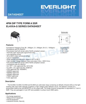
The pin configuration is clearly defined:
- Pin 1: LED Anode (+)
- Pin 2: LED Cathode (-)
- Pins 3 & 4: MOSFET Drain terminals (output switch). These are typically connected together on the PCB to handle the load current.
The device is marked on the top with a code: EL [Part Number] G YWWV.
Example: "EL 460A G YWWV" indicates an EL460A, halogen-free (G), with year (Y) and week (WW) of manufacture, and VDE option (V).
4.3 Recommended SMD Pad Layout
For the S1 (surface mount) option, a specific pad layout is recommended to ensure reliable soldering and mechanical strength. The dimensions ensure proper solder fillet formation and thermal relief during reflow.
5. Soldering & Assembly Guidelines
- Reflow Soldering (S1 Option): The device is rated for a peak soldering temperature of 260°C for 10 seconds. Standard lead-free reflow profiles (IPC/JEDEC J-STD-020) are applicable. Ensure the profile does not exceed the maximum temperature or time at peak temperature.
- Wave Soldering (DIP & M Options): Standard wave soldering processes can be used. Preheating is recommended to minimize thermal shock.
- Hand Soldering: Use a temperature-controlled iron. Limit contact time to prevent excessive heat transfer to the package.
- Cleaning: Compatible with most common flux cleaning processes. Verify compatibility if using aggressive solvents.
- Storage: Store in a dry, anti-static environment within the specified temperature range (-40°C to +125°C). For extended storage, follow moisture sensitivity level (MSL) guidelines, typically using dry-pack packaging for SMD parts.
6. Packaging & Ordering Information
6.1 Model Numbering System
The part number follows the format: EL4XXA(Y)(Z)-VG
- XX: Part number (06, 25, 40, 60) defining output voltage/current rating.
- Y: Lead form option (S1 for surface mount, or blank for standard DIP).
- Z: Tape and reel option (TA, TB, TU, TD, or blank for tube).
- V: Indicates VDE safety approval option.
- G: Denotes Halogen-Free construction.
6.2 Packing Specifications
- Tube Packaging: Standard DIP and Option M types are supplied in tubes of 100 units.
- Tape & Reel (S1 Option): Available in different reel types:
- TA, TB: 1000 units per reel.
- TU, TD: 1500 units per reel.
7. Application Design Considerations
7.1 Input Circuit Design
Drive the input LED with a constant current source or a voltage source with a series current-limiting resistor. Calculate the resistor value using: R = (Vcc - VF) / IF, where VF is typically 1.18V-1.5V and IF is chosen between 5mA and 20mA for optimal speed and reliability. Ensure the driving circuit can supply at least the minimum IF(on) (5mA max) to guarantee full output turn-on. A reverse protection diode across the LED is not strictly necessary due to the built-in 5V reverse voltage rating, but may be added for robustness in noisy environments.
7.2 Output Circuit Design
Voltage Selection: Choose the model (EL406A, 425A, 440A, 460A) based on the peak voltage (DC or AC) of your load, including any transients or surges. A safety derating of 20-30% is recommended.
Current and Power Dissipation: The key design constraint is power dissipation and heat. Power dissipated in the SSR (Pdiss) is calculated as: Pdiss = (IL^2 * Rd(ON)) + (IF * VF). The first term dominates. For example, running an EL406A at its maximum 550mA load with a typical Rd(ON) of 0.7Ω generates ~212mW of heat. Ensure the total power dissipation (Pout max 500mW) is not exceeded and that the PCB provides adequate thermal relief, especially for the higher current models.
Inductive/ Capacitive Loads: When switching inductive loads (relays, solenoids, motors), use a snubber circuit (RC network) or a flyback diode across the load to suppress voltage spikes that could exceed the device's VL rating. For capacitive loads, consider inrush current limiting.
7.3 Thermal Management
The SSR has no internal heatsink. Heat is conducted away through the leads. Use sufficient copper area on the PCB pads, especially for pins 3 and 4 (output), to act as a heatsink. For high ambient temperatures or continuous high-current operation, monitor the device temperature to ensure it stays within the operating range. The on-resistance will increase with temperature, creating a self-limiting effect but also reducing performance.
8. Technical Comparison & Selection Guide
The EL4XXA-G series offers a clear trade-off matrix:
- EL406A (60V, 550mA): Best choice for low-voltage, higher current DC switching (e.g., 12V/24V systems, battery-powered devices) where low voltage drop and power loss are critical. Has the lowest Rd(ON).
- EL425A (250V, 150mA) & EL440A (400V, 120mA): Ideal for mainstream AC line voltage applications (120VAC, 240VAC) switching small loads like indicators, small solenoids, or as pilot devices for larger contactors. The EL440A provides extra margin for 240VAC systems.
- EL460A (600V, 50mA): Designed for high-voltage industrial applications or situations with significant voltage transients. Suitable for switching signals or very low-power loads in high-voltage environments.
Compared to Electromechanical Relays (EMRs): These SSRs offer no moving parts, hence no contact bounce, arcing, or wear-out mechanisms related to cycle count. They operate silently and are immune to vibration. However, they have inherent on-resistance leading to heat generation and voltage drop, and typically have lower current ratings and higher cost per amp than comparable EMRs.
Compared to other SSRs: The photovoltaic MOSFET coupling scheme provides very high isolation and clean switching without the need for an external bias supply on the output side (unlike phototransistor or phototriac couplers). The turn-on speed is slower than some other opto-MOSFETs but is sufficient for most control applications.
9. Frequently Asked Questions (FAQ)
Q1: Can I use this SSR to switch AC loads directly?
A1: Yes, but with important caveats. The output is a pair of MOSFETs. Most MOSFETs have an inherent body diode. In a standard configuration, this SSR can block voltage of either polarity when off, but can only conduct current in one direction when on (like a diode). For true AC load switching, two devices would need to be configured in inverse series (back-to-back). Some SSRs have this configuration internally, but the EL4XXA-G datasheet shows a single MOSFET schematic, indicating it is for DC or unidirectional switching. Verify the specific model's capability for your AC application.
Q2: Why is the turn-on time much slower than the turn-off time?
A2: The turn-on time is limited by the speed at which the photovoltaic diode array can generate enough current to charge the gate capacitance of the output MOSFET to its threshold voltage. This is a relatively slow, current-limited process. Turn-off is fast because it only requires discharging the gate through the internal circuitry, which can be done quickly.
Q3: How do I interpret the "Pulse Load Current" rating?
A3: The pulse load current (ILPeak) is a higher current that can be handled for a very short duration (100ms, single pulse). This is useful for handling inrush currents from lamps or motors. Do not use this rating for continuous or repetitive pulsed operation. For repetitive pulses, the average power dissipation must remain within the Pout limit.
Q4: Is an external heatsink required?
A4: Typically not for the DIP package under its rated conditions. The primary heatsink is the PCB copper. For continuous operation at maximum load current, especially for the EL406A, ensure the PCB has adequate copper area (e.g., several square centimeters) connected to the output pins to dissipate heat. In confined spaces or high ambient temperatures, thermal analysis is recommended.
10. Design-in Case Study Example
Scenario: Designing a digital I/O module for a PLC that needs to switch 24VDC inductive loads (small solenoid valves) with a steady-state current of 200mA. The environment is industrially noisy.
Component Selection: The EL406A is chosen for its 60V rating (well above 24VDC) and low on-resistance. At 200mA, the typical voltage drop is only 200mA * 0.7Ω = 0.14V, and power dissipation is (0.2^2)*0.7 = 0.028W, which is negligible.
Input Circuit: The PLC's digital output is 24VDC. A series resistor is calculated: R = (24V - 1.3V) / 0.01A = 2270Ω. A standard 2.2kΩ resistor is selected, providing IF ≈ 10.3mA, safely above the maximum IF(on) of 5mA.
Output Circuit: A flyback diode (1N4007) is placed directly across the solenoid coil to clamp inductive kickback voltage and protect the EL406A's output. The diode cathode connects to the positive supply, anode to the SSR output/load connection.
PCB Layout: Pins 3 and 4 are connected to a large copper pour on the PCB to aid heat dissipation, though the heat generated is minimal in this case. The input and output traces are kept separate to maintain good isolation.
This design provides a robust, long-life, and silent switching solution compared to a small electromechanical relay.
11. Operating Principle
The EL4XXA-G operates on the principle of optical isolation and photovoltaic driving. When a forward current is applied to the input AlGaAs infrared LED, it emits light. This light is detected by a photovoltaic diode array on the output side. This array generates a small voltage (photovoltaic effect) when illuminated. This generated voltage is applied directly to the gate of one or more power MOSFETs, turning them on and creating a low-resistance path between the output pins (3 & 4). When the LED current is removed, the light stops, the photovoltaic voltage collapses, and the MOSFET gate discharges, turning the output off. This mechanism provides complete galvanic isolation between the low-voltage control circuit and the high-voltage load circuit, as only light crosses the isolation barrier.
12. Technology Trends
Solid-state relays continue to evolve in several key directions relevant to the EL4XXA-G's technology:
- Lower On-Resistance (Rd(ON)): Advances in MOSFET and packaging technology are steadily reducing the Rd(ON) for a given voltage rating and package size, enabling higher current switching in smaller footprints and with lower losses.
- Higher Integration: Trends include integrating input-side drivers (constant current sources, logic-level translators) and output-side protection features (overvoltage clamps, overtemperature shutdown) into the SSR package, simplifying external circuitry.
- Improved Thermal Performance: New package designs with exposed thermal pads (e.g., DIP packages with a bottom pad) allow for much more efficient heat transfer to the PCB, significantly increasing the continuous current rating for the same silicon.
- Wider Voltage Ranges: Devices capable of blocking higher voltages (1kV+) are becoming more common in compact packages, driven by applications in renewable energy and electric vehicles.
- Focus on Safety and Compliance: As with the EL4XXA-G, there is an increasing emphasis on meeting the latest international safety standards (UL, VDE, CQC), environmental regulations (halogen-free, RoHS), and automotive-grade qualifications for reliability.
The EL4XXA-G series represents a mature and reliable implementation of photovoltaic MOSFET SSR technology, well-suited for a broad range of industrial and commercial control applications requiring safe, isolated, and reliable low-to-medium power switching.
LED Specification Terminology
Complete explanation of LED technical terms
Photoelectric Performance
| Term | Unit/Representation | Simple Explanation | Why Important |
|---|---|---|---|
| Luminous Efficacy | lm/W (lumens per watt) | Light output per watt of electricity, higher means more energy efficient. | Directly determines energy efficiency grade and electricity cost. |
| Luminous Flux | lm (lumens) | Total light emitted by source, commonly called "brightness". | Determines if the light is bright enough. |
| Viewing Angle | ° (degrees), e.g., 120° | Angle where light intensity drops to half, determines beam width. | Affects illumination range and uniformity. |
| CCT (Color Temperature) | K (Kelvin), e.g., 2700K/6500K | Warmth/coolness of light, lower values yellowish/warm, higher whitish/cool. | Determines lighting atmosphere and suitable scenarios. |
| CRI / Ra | Unitless, 0–100 | Ability to render object colors accurately, Ra≥80 is good. | Affects color authenticity, used in high-demand places like malls, museums. |
| SDCM | MacAdam ellipse steps, e.g., "5-step" | Color consistency metric, smaller steps mean more consistent color. | Ensures uniform color across same batch of LEDs. |
| Dominant Wavelength | nm (nanometers), e.g., 620nm (red) | Wavelength corresponding to color of colored LEDs. | Determines hue of red, yellow, green monochrome LEDs. |
| Spectral Distribution | Wavelength vs intensity curve | Shows intensity distribution across wavelengths. | Affects color rendering and quality. |
Electrical Parameters
| Term | Symbol | Simple Explanation | Design Considerations |
|---|---|---|---|
| Forward Voltage | Vf | Minimum voltage to turn on LED, like "starting threshold". | Driver voltage must be ≥Vf, voltages add up for series LEDs. |
| Forward Current | If | Current value for normal LED operation. | Usually constant current drive, current determines brightness & lifespan. |
| Max Pulse Current | Ifp | Peak current tolerable for short periods, used for dimming or flashing. | Pulse width & duty cycle must be strictly controlled to avoid damage. |
| Reverse Voltage | Vr | Max reverse voltage LED can withstand, beyond may cause breakdown. | Circuit must prevent reverse connection or voltage spikes. |
| Thermal Resistance | Rth (°C/W) | Resistance to heat transfer from chip to solder, lower is better. | High thermal resistance requires stronger heat dissipation. |
| ESD Immunity | V (HBM), e.g., 1000V | Ability to withstand electrostatic discharge, higher means less vulnerable. | Anti-static measures needed in production, especially for sensitive LEDs. |
Thermal Management & Reliability
| Term | Key Metric | Simple Explanation | Impact |
|---|---|---|---|
| Junction Temperature | Tj (°C) | Actual operating temperature inside LED chip. | Every 10°C reduction may double lifespan; too high causes light decay, color shift. |
| Lumen Depreciation | L70 / L80 (hours) | Time for brightness to drop to 70% or 80% of initial. | Directly defines LED "service life". |
| Lumen Maintenance | % (e.g., 70%) | Percentage of brightness retained after time. | Indicates brightness retention over long-term use. |
| Color Shift | Δu′v′ or MacAdam ellipse | Degree of color change during use. | Affects color consistency in lighting scenes. |
| Thermal Aging | Material degradation | Deterioration due to long-term high temperature. | May cause brightness drop, color change, or open-circuit failure. |
Packaging & Materials
| Term | Common Types | Simple Explanation | Features & Applications |
|---|---|---|---|
| Package Type | EMC, PPA, Ceramic | Housing material protecting chip, providing optical/thermal interface. | EMC: good heat resistance, low cost; Ceramic: better heat dissipation, longer life. |
| Chip Structure | Front, Flip Chip | Chip electrode arrangement. | Flip chip: better heat dissipation, higher efficacy, for high-power. |
| Phosphor Coating | YAG, Silicate, Nitride | Covers blue chip, converts some to yellow/red, mixes to white. | Different phosphors affect efficacy, CCT, and CRI. |
| Lens/Optics | Flat, Microlens, TIR | Optical structure on surface controlling light distribution. | Determines viewing angle and light distribution curve. |
Quality Control & Binning
| Term | Binning Content | Simple Explanation | Purpose |
|---|---|---|---|
| Luminous Flux Bin | Code e.g., 2G, 2H | Grouped by brightness, each group has min/max lumen values. | Ensures uniform brightness in same batch. |
| Voltage Bin | Code e.g., 6W, 6X | Grouped by forward voltage range. | Facilitates driver matching, improves system efficiency. |
| Color Bin | 5-step MacAdam ellipse | Grouped by color coordinates, ensuring tight range. | Guarantees color consistency, avoids uneven color within fixture. |
| CCT Bin | 2700K, 3000K etc. | Grouped by CCT, each has corresponding coordinate range. | Meets different scene CCT requirements. |
Testing & Certification
| Term | Standard/Test | Simple Explanation | Significance |
|---|---|---|---|
| LM-80 | Lumen maintenance test | Long-term lighting at constant temperature, recording brightness decay. | Used to estimate LED life (with TM-21). |
| TM-21 | Life estimation standard | Estimates life under actual conditions based on LM-80 data. | Provides scientific life prediction. |
| IESNA | Illuminating Engineering Society | Covers optical, electrical, thermal test methods. | Industry-recognized test basis. |
| RoHS / REACH | Environmental certification | Ensures no harmful substances (lead, mercury). | Market access requirement internationally. |
| ENERGY STAR / DLC | Energy efficiency certification | Energy efficiency and performance certification for lighting. | Used in government procurement, subsidy programs, enhances competitiveness. |