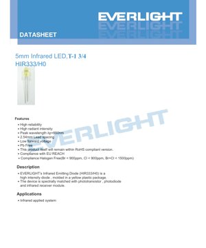
1. Product Overview
The HIR333/H0 is a high-intensity infrared emitting diode housed in a standard T-1 3/4 (5mm) through-hole package with a yellow plastic lens. The device is engineered to deliver reliable performance in infrared sensing and communication systems. Its primary function is to emit infrared light at a peak wavelength of 850nm, which is spectrally optimized for compatibility with common silicon-based photodetectors such as phototransistors, photodiodes, and integrated infrared receiver modules. The product is designed with a focus on high reliability and consistent output.
1.1 Core Advantages and Target Market
The key advantages of this component include its high radiant intensity, which enables strong signal transmission, and its low forward voltage, contributing to energy-efficient operation. It is constructed using lead-free materials and complies with major environmental and safety directives including RoHS, EU REACH, and halogen-free standards (Br < 900ppm, Cl < 900ppm, Br+Cl < 1500ppm). These features make it suitable for a wide range of commercial and industrial infrared applications where regulatory compliance and long-term reliability are critical. The target market includes manufacturers of security systems, remote controls, optical switches, object detection sensors, and various consumer electronics requiring non-visible light sources.
2. In-Depth Technical Parameter Analysis
This section provides a detailed breakdown of the electrical, optical, and thermal specifications that define the operational boundaries and performance of the LED.
2.1 Absolute Maximum Ratings
The Absolute Maximum Ratings define the stress limits beyond which permanent damage to the device may occur. These ratings should never be exceeded, even momentarily. Operation should be maintained within the recommended operating conditions for reliable performance.
- Continuous Forward Current (IF): 100 mA. This is the maximum DC current that can be continuously applied to the LED.
- Peak Forward Current (IFP): 1.0 A. This high current is permissible only under pulsed conditions with a pulse width ≤ 100μs and a duty cycle ≤ 1% to prevent overheating.
- Reverse Voltage (VR): 5 V. Exceeding this reverse bias voltage can cause junction breakdown.
- Power Dissipation (Pd): 150 mW at or below 25°C free air temperature. This rating decreases with increasing ambient temperature.
- Temperature Ranges: Operating: -40°C to +85°C; Storage: -40°C to +100°C.
- Soldering Temperature (Tsol): 260°C for a maximum of 5 seconds, defining the limits for wave or reflow soldering processes.
2.2 Electro-Optical Characteristics
The Electro-Optical Characteristics are specified at a standard test condition of an ambient temperature (Ta) of 25°C. These parameters define the typical performance of the device.
- Radiant Intensity (Ie): This is the optical power emitted per unit solid angle, measured in milliwatts per steradian (mW/sr). The typical value is 15 mW/sr at a forward current (IF) of 20mA. Under a pulsed current of 100mA, the radiant intensity can reach 80 mW/sr.
- Peak Wavelength (λp): 850 nm (typical). This is the wavelength at which the optical output power is at its maximum. This wavelength is invisible to the human eye but is efficiently detected by silicon sensors.
- Spectral Bandwidth (Δλ): 45 nm (typical). This indicates the range of wavelengths the LED emits, measured at half the maximum intensity (Full Width at Half Maximum - FWHM).
- Forward Voltage (VF): 1.45V (typical) at IF=20mA, with a maximum of 1.65V. At IF=100mA (pulsed), the typical VF rises to 1.80V with a maximum of 2.40V.
- Reverse Current (IR): Maximum 10 μA at VR=5V, indicating very low leakage in the off-state.
- View Angle (2θ1/2): 30 degrees (typical). This is the full angle at which the radiant intensity drops to half of its value at the center (0°). A 30° angle provides a moderately focused beam.
3. Binning System Explanation
The radiant intensity of the LEDs is sorted into different bins or ranks to ensure consistency for the end-user. The binning is performed under a standard test condition of IF = 20mA. The available bins are defined by a letter code (M, N, P, Q, R) with corresponding minimum and maximum radiant intensity values. This allows designers to select a component that meets their specific sensitivity or range requirements. For example, selecting a 'P' bin guarantees a minimum radiant intensity of 15.0 mW/sr and a maximum of 24.0 mW/sr. The datasheet does not indicate separate binning for wavelength (Hue) or forward voltage (REF) for this specific part number, but the label specification suggests these parameters are tracked during manufacturing.
4. Performance Curve Analysis
The typical performance curves provide visual insights into the device's behavior under varying conditions, which is crucial for circuit design and thermal management.
4.1 Forward Current vs. Ambient Temperature
This derating curve shows how the maximum allowable continuous forward current decreases as the ambient temperature increases above 25°C. To ensure the junction temperature remains within safe limits and to maintain long-term reliability, the operating current must be reduced in high-temperature environments. Designers must consult this curve when operating the LED in enclosures or at elevated ambient temperatures.
4.2 Spectral Distribution
The spectral distribution graph plots the relative radiant intensity against wavelength. It visually confirms the peak wavelength at 850nm and the approximately 45nm spectral bandwidth. The curve is characteristic of GaAlAs (Gallium Aluminum Arsenide) semiconductor material. The narrow, well-defined peak ensures minimal overlap with visible light and optimal coupling with silicon detectors, which have peak sensitivity around 800-900nm.
4.3 Radiant Intensity vs. Forward Current
This curve illustrates the relationship between the drive current and the optical output. The radiant intensity increases super-linearly with current at lower levels and tends to become more linear at higher currents, eventually saturating as internal efficiency drops due to heating effects. The curve for the pulsed condition (100mA) shows significantly higher output than the DC condition, highlighting the benefit of pulsed operation for achieving high peak intensity without thermal damage.
4.4 Relative Radiant Intensity vs. Angular Displacement
This polar plot depicts the spatial emission pattern of the LED. It shows how the light intensity diminishes as the viewing angle moves away from the central axis (0°). The pattern is roughly Lambertian for this package type, with the intensity at the half-angle points (approximately ±15°) being 50% of the on-axis intensity, defining the 30° view angle.
5. Mechanical and Package Information
The device uses a standard 5mm (T-1 3/4) radial leaded package. The leads have a standard 2.54mm (0.1 inch) spacing, compatible with common perforated prototyping boards and PCB layouts. The package dimension drawing provides critical measurements including the overall diameter, lens height, lead length, and lead diameter. The body is molded from yellow plastic, which is transparent to the 850nm infrared light but appears colored to aid in visual identification and differentiation from visible-light LEDs. The cathode is typically identified by a flat spot on the lens rim and/or a shorter lead. All dimensions have a standard tolerance of ±0.25mm unless otherwise specified.
6. Soldering and Assembly Guidelines
Proper handling during assembly is essential to prevent mechanical or thermal damage to the LED.
6.1 Lead Forming
If leads need to be bent, it must be done at a point at least 3mm away from the base of the epoxy bulb. Forming should always be performed before soldering, at room temperature, and with care to avoid applying stress directly to the epoxy body, which can crack the package or damage the internal wire bonds. PCB holes must align precisely with the LED leads to avoid mounting stress.
6.2 Storage
LEDs should be stored in a cool, dry environment (≤30°C, ≤70% Relative Humidity). The recommended storage life after shipment is 3 months. For longer storage (up to one year), the components should be kept in a sealed, moisture-barrier bag with desiccant, preferably in a nitrogen atmosphere, to prevent moisture absorption and potential \"popcorning\" during soldering.
6.3 Soldering Process
A minimum distance of 3mm must be maintained between the solder joint and the epoxy bulb. Recommended soldering parameters are:
Hand Soldering: Iron tip temperature ≤300°C (for a 30W max iron), soldering time ≤3 seconds per lead.
Wave/Dip Soldering: Preheat temperature ≤100°C for ≤60 seconds; solder bath temperature ≤260°C for ≤5 seconds.
The provided soldering profile graph recommends a rapid temperature ramp-up, a plateau (soak) zone, a brief peak at 260°C, and a controlled cooldown. Rapid cooling or thermal shock should be avoided. Re-soldering (more than one cycle of dip or hand soldering) is not recommended.
6.4 Cleaning
If cleaning is necessary after soldering, use isopropyl alcohol at room temperature for no more than one minute. Do not use ultrasonic cleaning unless its effects (power, frequency, duration) have been thoroughly pre-qualified on sample assemblies, as ultrasonic energy can fracture the delicate internal semiconductor structure.
5.5 Heat Management
Effective thermal management is a critical design consideration. The power dissipation rating of 150mW is specified at 25°C. In real applications, the actual power dissipated (VF * IF) must be derated as ambient temperature rises, as shown in the derating curve. For continuous operation at high currents or in high ambient temperatures, consider using a heatsink, increasing airflow, or implementing pulsed drive to reduce average junction temperature and ensure long-term reliability.
7. Packaging and Ordering Information
The LEDs are packaged in anti-static bags to protect them from electrostatic discharge (ESD). These bags are placed inside inner cartons, which are then packed into larger outside cartons for shipping. A typical packing quantity is 200-500 pieces per bag, with 5 bags per inner carton, and 10 inner cartons per master outside carton. The label on the bag contains key information for traceability and identification, including the Customer's Product Number (CPN), the manufacturer's Product Number (P/N), packing Quantity (QTY), and the Luminous Intensity Rank (CAT). Other codes may indicate Dominant Wavelength Rank (HUE), Forward Voltage Rank (REF), Lot Number, and Date Code.
8. Application Suggestions and Design Considerations
8.1 Typical Application Scenarios
- Infrared Remote Controls: Used as the transmitter in TV, audio, and set-top box remotes.
- Proximity and Object Detection: Paired with a phototransistor to sense the presence, absence, or position of an object.
- Optical Switches: Used in slot sensors (e.g., paper detection in printers) or reflective sensors.
- Security Systems: For night vision illumination in CCTV cameras or as part of infrared intrusion detection beams.
- Industrial Automation: For non-contact sensing in counting, alignment, and level detection applications.
8.2 Design Considerations
- Current Limiting: Always use a series resistor or constant current driver to limit the forward current to the desired value, calculated based on the supply voltage and the LED's forward voltage.
- Pulsed Operation: For applications requiring high peak intensity (like long-range sensing), use pulsed drive with appropriate duty cycle to stay within the peak current and average power ratings.
- Optical Design: Consider the 30° view angle when designing lenses, apertures, or optical paths. For longer range, external lenses can be used to collimate the beam.
- Detector Matching: Ensure the selected photodetector (phototransistor, photodiode, or receiver IC) has high sensitivity in the 850nm region.
- Ambient Light Immunity: In environments with strong ambient light (especially sunlight containing IR), use modulated (pulsed) IR signals and synchronous detection in the receiver to distinguish the signal from background noise.
9. Technical Comparison and Differentiation
Compared to standard visible-light LEDs, this IR LED is optimized for output in the infrared spectrum with a material (GaAlAs) that provides high efficiency at 850nm. Its key differentiators within the IR LED category are its combination of relatively high radiant intensity (15 mW/sr typical) and low forward voltage (1.45V typical), which can lead to lower power consumption in battery-operated devices. The 30° viewing angle offers a good balance between beam concentration and coverage area. Compliance with modern environmental standards (RoHS, REACH, Halogen-Free) is a significant advantage for products destined for global markets, eliminating material compliance concerns.
10. Frequently Asked Questions Based on Technical Parameters
Q: Can I drive this LED directly from a 5V supply?
A: No. You must use a current-limiting resistor. For example, with a 5V supply and a target current of 20mA, and assuming a typical VF of 1.45V, the resistor value would be R = (5V - 1.45V) / 0.02A = 177.5Ω. A standard 180Ω resistor would be suitable.
Q: What is the difference between the DC and pulsed radiant intensity ratings?
A: The DC rating (15 mW/sr at 20mA) is for continuous operation where thermal effects limit the output. The pulsed rating (80 mW/sr at 100mA) is achievable because the brief pulse does not allow the junction to heat up significantly, allowing much higher instantaneous current and thus higher light output.
Q: How do I identify the cathode?
A: In a standard 5mm package, the cathode is typically indicated by two features: 1) A flat edge on the round plastic lens rim. 2) The cathode lead is usually shorter than the anode lead. Always verify the polarity before soldering.
Q: Is this LED sensitive to ESD?
A> Like all semiconductor devices, it can be damaged by electrostatic discharge. It is supplied in anti-static packaging and should be handled with appropriate ESD precautions during assembly.
11. Practical Design and Usage Case
Case: Designing a Simple Object Detection Sensor
A common application is a break-beam sensor. The HIR333/H0 IR LED is placed on one side of a path, and a phototransistor is placed directly opposite. When an object passes between them, it interrupts the infrared beam, causing the phototransistor's output to change. For this design:
1. Drive the LED with a 20mA constant current using a simple transistor switch or a microcontroller GPIO pin (with series resistor).
2. For improved noise immunity and range, pulse the LED at a frequency (e.g., 38kHz) and use a phototransistor module with a built-in 38kHz filter.
3. Align the LED and detector carefully, considering the 30° emission cone. For longer gaps, consider adding a tube or collimating lens in front of the LED to narrow the beam.
4. Place the sensor away from direct sunlight or other strong sources of infrared light to prevent false triggers.
12. Principle of Operation Introduction
An Infrared Light Emitting Diode (IR LED) is a semiconductor p-n junction diode. When a forward voltage is applied, electrons from the n-region and holes from the p-region are injected across the junction. When these charge carriers recombine in the active region, energy is released in the form of photons (light). The wavelength (color) of the emitted light is determined by the bandgap energy of the semiconductor material. The HIR333/H0 uses Gallium Aluminum Arsenide (GaAlAs), which has a bandgap corresponding to photons in the near-infrared spectrum, specifically around 850 nanometers. The yellow plastic package is doped to be transparent to this wavelength while blocking visible light, and it also acts as a primary lens to shape the output beam.
13. Technology Trends and Developments
The trend in infrared LED technology continues towards higher efficiency (more light output per electrical watt input) and higher power densities. This allows for either brighter sources or more energy-efficient designs. There is also development in varying peak wavelengths; while 850nm and 940nm are common, other wavelengths are being optimized for specific applications like gas sensing or medical diagnostics. Packaging is evolving to support surface-mount technology (SMD) for automated assembly, though through-hole packages like the 5mm remain popular for prototyping, repair, and certain high-reliability applications. Integration is another trend, with IR LEDs being combined with drivers, modulators, and even detectors into single modules to simplify system design for the end user.
LED Specification Terminology
Complete explanation of LED technical terms
Photoelectric Performance
| Term | Unit/Representation | Simple Explanation | Why Important |
|---|---|---|---|
| Luminous Efficacy | lm/W (lumens per watt) | Light output per watt of electricity, higher means more energy efficient. | Directly determines energy efficiency grade and electricity cost. |
| Luminous Flux | lm (lumens) | Total light emitted by source, commonly called "brightness". | Determines if the light is bright enough. |
| Viewing Angle | ° (degrees), e.g., 120° | Angle where light intensity drops to half, determines beam width. | Affects illumination range and uniformity. |
| CCT (Color Temperature) | K (Kelvin), e.g., 2700K/6500K | Warmth/coolness of light, lower values yellowish/warm, higher whitish/cool. | Determines lighting atmosphere and suitable scenarios. |
| CRI / Ra | Unitless, 0–100 | Ability to render object colors accurately, Ra≥80 is good. | Affects color authenticity, used in high-demand places like malls, museums. |
| SDCM | MacAdam ellipse steps, e.g., "5-step" | Color consistency metric, smaller steps mean more consistent color. | Ensures uniform color across same batch of LEDs. |
| Dominant Wavelength | nm (nanometers), e.g., 620nm (red) | Wavelength corresponding to color of colored LEDs. | Determines hue of red, yellow, green monochrome LEDs. |
| Spectral Distribution | Wavelength vs intensity curve | Shows intensity distribution across wavelengths. | Affects color rendering and quality. |
Electrical Parameters
| Term | Symbol | Simple Explanation | Design Considerations |
|---|---|---|---|
| Forward Voltage | Vf | Minimum voltage to turn on LED, like "starting threshold". | Driver voltage must be ≥Vf, voltages add up for series LEDs. |
| Forward Current | If | Current value for normal LED operation. | Usually constant current drive, current determines brightness & lifespan. |
| Max Pulse Current | Ifp | Peak current tolerable for short periods, used for dimming or flashing. | Pulse width & duty cycle must be strictly controlled to avoid damage. |
| Reverse Voltage | Vr | Max reverse voltage LED can withstand, beyond may cause breakdown. | Circuit must prevent reverse connection or voltage spikes. |
| Thermal Resistance | Rth (°C/W) | Resistance to heat transfer from chip to solder, lower is better. | High thermal resistance requires stronger heat dissipation. |
| ESD Immunity | V (HBM), e.g., 1000V | Ability to withstand electrostatic discharge, higher means less vulnerable. | Anti-static measures needed in production, especially for sensitive LEDs. |
Thermal Management & Reliability
| Term | Key Metric | Simple Explanation | Impact |
|---|---|---|---|
| Junction Temperature | Tj (°C) | Actual operating temperature inside LED chip. | Every 10°C reduction may double lifespan; too high causes light decay, color shift. |
| Lumen Depreciation | L70 / L80 (hours) | Time for brightness to drop to 70% or 80% of initial. | Directly defines LED "service life". |
| Lumen Maintenance | % (e.g., 70%) | Percentage of brightness retained after time. | Indicates brightness retention over long-term use. |
| Color Shift | Δu′v′ or MacAdam ellipse | Degree of color change during use. | Affects color consistency in lighting scenes. |
| Thermal Aging | Material degradation | Deterioration due to long-term high temperature. | May cause brightness drop, color change, or open-circuit failure. |
Packaging & Materials
| Term | Common Types | Simple Explanation | Features & Applications |
|---|---|---|---|
| Package Type | EMC, PPA, Ceramic | Housing material protecting chip, providing optical/thermal interface. | EMC: good heat resistance, low cost; Ceramic: better heat dissipation, longer life. |
| Chip Structure | Front, Flip Chip | Chip electrode arrangement. | Flip chip: better heat dissipation, higher efficacy, for high-power. |
| Phosphor Coating | YAG, Silicate, Nitride | Covers blue chip, converts some to yellow/red, mixes to white. | Different phosphors affect efficacy, CCT, and CRI. |
| Lens/Optics | Flat, Microlens, TIR | Optical structure on surface controlling light distribution. | Determines viewing angle and light distribution curve. |
Quality Control & Binning
| Term | Binning Content | Simple Explanation | Purpose |
|---|---|---|---|
| Luminous Flux Bin | Code e.g., 2G, 2H | Grouped by brightness, each group has min/max lumen values. | Ensures uniform brightness in same batch. |
| Voltage Bin | Code e.g., 6W, 6X | Grouped by forward voltage range. | Facilitates driver matching, improves system efficiency. |
| Color Bin | 5-step MacAdam ellipse | Grouped by color coordinates, ensuring tight range. | Guarantees color consistency, avoids uneven color within fixture. |
| CCT Bin | 2700K, 3000K etc. | Grouped by CCT, each has corresponding coordinate range. | Meets different scene CCT requirements. |
Testing & Certification
| Term | Standard/Test | Simple Explanation | Significance |
|---|---|---|---|
| LM-80 | Lumen maintenance test | Long-term lighting at constant temperature, recording brightness decay. | Used to estimate LED life (with TM-21). |
| TM-21 | Life estimation standard | Estimates life under actual conditions based on LM-80 data. | Provides scientific life prediction. |
| IESNA | Illuminating Engineering Society | Covers optical, electrical, thermal test methods. | Industry-recognized test basis. |
| RoHS / REACH | Environmental certification | Ensures no harmful substances (lead, mercury). | Market access requirement internationally. |
| ENERGY STAR / DLC | Energy efficiency certification | Energy efficiency and performance certification for lighting. | Used in government procurement, subsidy programs, enhances competitiveness. |