Table of Contents
- 1. Product Overview
- 2. Technical Parameter Deep-Dive
- 2.1 Absolute Maximum Ratings
- 2.2 Electro-Optical Characteristics
- 3. Performance Curve Analysis
- 3.1 Spectral Sensitivity
- 3.2 Temperature Dependence
- 3.3 Linearity and Dynamic Response
- 3.4 Capacitance vs. Voltage
- 4. Mechanical and Packaging Information
- 4.1 Package Dimension
- 4.2 Polarity Identification
- 5. Soldering and Assembly Guidelines
- 6. Packaging and Ordering Information
- 6.1 Packing Specification
- 6.2 Label Specification
- 7. Application Suggestions
- 7.1 Typical Application Scenarios
- 7.2 Design Considerations
- 8. Technical Comparison and Differentiation
- 9. Frequently Asked Questions (Based on Technical Parameters)
- 9.1 What is the difference between short-circuit current (ISC) and reverse light current (IL)?
- 9.2 Why is the dark current important?
- 9.3 How do I choose the load resistor (RL) for my application?
- 9.4 Can I use this with a visible light source like a red LED?
- 10. Design and Usage Case Study
- 11. Operating Principle
- 12. Technology Trends
1. Product Overview
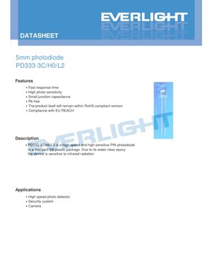
The PD333-3C/H0/L2 is a high-speed, high-sensitivity silicon PIN photodiode housed in a standard 5mm diameter plastic package. This device is designed for applications requiring fast optical detection, leveraging its small junction capacitance and fast response time. The use of water-clear epoxy as the lens material makes it sensitive to a broad spectrum, including visible and infrared radiation, with a peak sensitivity specifically in the near-infrared region. Its primary design goals are to provide reliable performance in compact, cost-effective sensing solutions.
2. Technical Parameter Deep-Dive
This section provides an objective analysis of the key electrical and optical parameters specified in the datasheet.
2.1 Absolute Maximum Ratings
The device is rated for a maximum reverse voltage (VR) of 32V, which defines the upper limit of the bias voltage that can be applied without risking permanent damage. The operating temperature range (Topr) is from -25°C to +85°C, suitable for most commercial and industrial environments. Storage can occur in a wider range from -40°C to +100°C. The soldering temperature (Tsol) is specified at 260°C, which is a standard peak temperature for lead-free reflow processes. The power dissipation (Pc) is 150 mW at or below 25°C ambient temperature, a parameter crucial for thermal management in the application circuit.
2.2 Electro-Optical Characteristics
The spectral response is broad, covering a bandwidth (λ0.5) from 400 nm to 1100 nm, with a typical peak sensitivity wavelength (λP) at 940 nm. This makes it ideal for infrared sensing applications, such as those using 850nm or 940nm IR LEDs. Key sensitivity parameters include a typical open-circuit voltage (VOC) of 0.39V and a short-circuit current (ISC) of 40 μA, both measured under an irradiance (Ee) of 1 mW/cm² at 940nm. Under a 5V reverse bias, the typical reverse light current (IL) is 40 μA under the same irradiance condition. The reverse dark current (ID), a critical parameter for low-light performance, is typically 5 nA at VR=10V, with a maximum of 30 nA. The total junction capacitance (Ct) is typically 18 pF at VR=5V and 1 MHz, which directly influences the device's speed. The rise and fall times (tr/tf) are typically 45 ns each when measured with VR=10V and a 100Ω load resistor (RL), confirming its high-speed capability. The viewing angle (2θ1/2) is 80 degrees.
3. Performance Curve Analysis
The datasheet includes several typical performance curves that illustrate how key parameters vary with operating conditions. These curves are essential for design engineers to predict real-world performance.
3.1 Spectral Sensitivity
The spectral sensitivity curve shows the relative responsivity of the photodiode across wavelengths from approximately 400 nm to 1100 nm. The curve peaks sharply around 940 nm, confirming its optimization for near-infrared light. Sensitivity drops significantly in the deep visible and beyond 1100 nm.
3.2 Temperature Dependence
Two curves highlight temperature effects: Power Dissipation vs. Ambient Temperature and Reverse Dark Current vs. Ambient Temperature. The power dissipation derating curve shows how the maximum allowable power decreases as ambient temperature increases above 25°C. The dark current curve demonstrates that ID increases exponentially with temperature, a common characteristic of semiconductor junctions. This is critical for applications operating at elevated temperatures, as increased dark current raises the noise floor.
3.3 Linearity and Dynamic Response
The Reverse Light Current vs. Ee curve illustrates the photodiode's linearity. Over a specified range of irradiance, the photocurrent (IL) should increase linearly with incident optical power. The Response Time vs. Load Resistance curve shows how the rise/fall time (tr/tf) increases with higher load resistance (RL). For high-speed applications, a low-value load resistor (like the 100Ω used in the spec) is necessary, though it produces a smaller output voltage swing.
3.4 Capacitance vs. Voltage
The Terminal Capacitance vs. Reverse Voltage curve shows that the junction capacitance (Ct) decreases as the reverse bias voltage increases. This is due to the widening of the depletion region. Applying a higher reverse bias (within limits) can thus improve speed by reducing capacitance, at the cost of potentially higher dark current.
4. Mechanical and Packaging Information
4.1 Package Dimension
The device uses a standard radial-leaded 5mm (T-1 3/4) package. The detailed dimension drawing specifies the diameter, lead spacing, lead length, and lens shape. A key note specifies that dimensional tolerances are ±0.25mm unless otherwise stated. The anode and cathode are identified, with the longer lead typically being the anode (positive side in photovoltaic mode).
4.2 Polarity Identification
Polarity is indicated by lead length. The longer lead is the anode (P-side), and the shorter lead is the cathode (N-side). When operated in photoconductive mode (reverse biased), the cathode should be connected to the positive supply voltage.
5. Soldering and Assembly Guidelines
The absolute maximum rating for soldering temperature is 260°C. This aligns with common lead-free reflow profiles. During hand soldering, care should be taken to minimize the heat exposure time to prevent damage to the plastic package and the epoxy lens. The device should be stored in conditions within the specified storage temperature range (-40°C to +100°C) and in a dry environment to prevent moisture absorption, which could affect reliability during reflow.
6. Packaging and Ordering Information
6.1 Packing Specification
The standard packing method is: 200-500 pieces per bag, 5 bags per inner carton, and 10 inner cartons per master (outside) carton.
6.2 Label Specification
The label on the packaging contains several fields: CPN (Customer's Product Number), P/N (Product Number), QTY (Packing Quantity), LOT No. (Lot Number for traceability), and date codes. This facilitates inventory management and traceability.
7. Application Suggestions
7.1 Typical Application Scenarios
The datasheet lists: High-speed photo detection, Security systems, and Cameras. Specifically, this photodiode is well-suited for:
- Infrared Remote Control Receivers: Paired with a 940nm IR LED and a demodulating IC.
- Optical Encoders: For speed and position sensing in printers, motors, or industrial equipment.
- Ambient Light Sensing (ALS): For display backlight control in devices, though its IR sensitivity may require filtering for accurate visible light measurement.
- Simple Object Detection: In conjunction with an IR light source for proximity sensing or break-beam sensors.
- Pulse Oximetry (in medical devices, with appropriate qualifications): Sensing red and IR light, though medical certification is required.
7.2 Design Considerations
Bias Configuration: For high-speed or linear response, use the photodiode in photoconductive mode (reverse biased). A transimpedance amplifier (TIA) circuit is commonly used to convert the photocurrent into a voltage. The feedback resistor and capacitor in the TIA must be chosen based on the desired bandwidth and the photodiode's capacitance (18 pF typical).
Noise Minimization: Keep the photodiode leads short and use a guarded layout to minimize parasitic capacitance and pick-up of electromagnetic interference. For low-light applications, consider cooling the device to reduce dark current noise.
Optical Considerations: The water-clear lens admits visible and IR light. If only IR detection is desired, an IR-pass filter can be added to block visible light and reduce noise from ambient visible sources. The 80-degree viewing angle provides a wide field of view; optical apertures or lenses can be used to narrow it if needed.
8. Technical Comparison and Differentiation
Compared to a standard PN photodiode, a PIN photodiode like the PD333-3C/H0/L2 has an intrinsic (I) region between the P and N layers. This intrinsic region creates a larger depletion area, which results in two key advantages: 1) Lower Junction Capacitance: The 18 pF capacitance is relatively low for a 5mm device, enabling faster response times. 2) Improved Linearity: The wider depletion region allows for more efficient charge carrier collection across a wider range of bias voltages and light intensities. Compared to phototransistors, photodiodes are generally faster and have a more linear output but produce a much smaller current signal, requiring more sophisticated amplification.
9. Frequently Asked Questions (Based on Technical Parameters)
9.1 What is the difference between short-circuit current (ISC) and reverse light current (IL)?
ISC is measured with zero bias across the diode (photovoltaic mode), while IL is measured under a specified reverse bias (photoconductive mode). IL is typically very close to, but not exactly the same as, ISC. The datasheet shows both as 40 μA typical under the same test conditions.
9.2 Why is the dark current important?
Dark current is the small current that flows even when no light is present. It sets the noise floor for the sensor. In low-light applications, a low dark current (5 nA typical here) is essential for achieving a good signal-to-noise ratio.
9.3 How do I choose the load resistor (RL) for my application?
The choice involves a trade-off between speed and output amplitude. A small RL (e.g., 50Ω) gives fast response (see the tr/tf vs. RL curve) but a small output voltage (Vout = IL * RL). A large RL gives a larger voltage but slower response due to the RC time constant formed by the photodiode capacitance and RL. For digital pulse detection, speed is often prioritized.
9.4 Can I use this with a visible light source like a red LED?
Yes, the spectral response curve shows significant sensitivity down to 400 nm. However, its responsivity at 650 nm (red) will be lower than at its 940 nm peak. You would get a smaller signal compared to using an IR source of the same optical power.
10. Design and Usage Case Study
Case: Designing an Infrared Data Link Receiver. A designer needs to receive modulated data from a 940nm IR LED at 38 kHz (a common remote control frequency). They select the PD333-3C/H0/L2 for its high sensitivity at 940nm and fast response (45 ns rise time is more than sufficient for 38 kHz). The photodiode is reverse-biased at 5V. The output is connected to a dedicated IR receiver IC (which includes a TIA, bandpass filter tuned to 38 kHz, and demodulator). The designer places the photodiode close to the IC's input pin, uses short traces, and adds a small decoupling capacitor near the bias supply to minimize noise. An IR-transparent window is placed in front of the photodiode to block visible light and reduce interference from fluorescent lights, which can flicker at 100/120 Hz.
11. Operating Principle
A PIN photodiode is a semiconductor device that converts light into electrical current. When photons with energy greater than the semiconductor's bandgap strike the device, they generate electron-hole pairs in the intrinsic region. Under the influence of the built-in electric field (in photovoltaic mode) or an applied reverse bias (in photoconductive mode), these charge carriers are swept apart, creating a measurable photocurrent that is proportional to the incident optical power. The "I" (intrinsic) layer is key: it is lightly doped, creating a wide depletion region that reduces capacitance for higher speed and improves quantum efficiency by providing a larger volume for photon absorption.
12. Technology Trends
The general trend in photodiode technology is toward higher integration, lower noise, and greater application specificity. This includes the development of photodiodes with on-chip amplification (integrated photodiode-amplifier combinations), arrays for imaging or multi-channel sensing, and devices with tailored spectral responses or built-in optical filters. There is also ongoing research into materials beyond silicon (like InGaAs) for extended infrared range detection. For standard commercial components like the 5mm PIN photodiode, the focus remains on cost reduction, reliability improvement, and achieving tighter parameter distributions while maintaining key performance metrics like speed and sensitivity.
LED Specification Terminology
Complete explanation of LED technical terms
Photoelectric Performance
| Term | Unit/Representation | Simple Explanation | Why Important |
|---|---|---|---|
| Luminous Efficacy | lm/W (lumens per watt) | Light output per watt of electricity, higher means more energy efficient. | Directly determines energy efficiency grade and electricity cost. |
| Luminous Flux | lm (lumens) | Total light emitted by source, commonly called "brightness". | Determines if the light is bright enough. |
| Viewing Angle | ° (degrees), e.g., 120° | Angle where light intensity drops to half, determines beam width. | Affects illumination range and uniformity. |
| CCT (Color Temperature) | K (Kelvin), e.g., 2700K/6500K | Warmth/coolness of light, lower values yellowish/warm, higher whitish/cool. | Determines lighting atmosphere and suitable scenarios. |
| CRI / Ra | Unitless, 0–100 | Ability to render object colors accurately, Ra≥80 is good. | Affects color authenticity, used in high-demand places like malls, museums. |
| SDCM | MacAdam ellipse steps, e.g., "5-step" | Color consistency metric, smaller steps mean more consistent color. | Ensures uniform color across same batch of LEDs. |
| Dominant Wavelength | nm (nanometers), e.g., 620nm (red) | Wavelength corresponding to color of colored LEDs. | Determines hue of red, yellow, green monochrome LEDs. |
| Spectral Distribution | Wavelength vs intensity curve | Shows intensity distribution across wavelengths. | Affects color rendering and quality. |
Electrical Parameters
| Term | Symbol | Simple Explanation | Design Considerations |
|---|---|---|---|
| Forward Voltage | Vf | Minimum voltage to turn on LED, like "starting threshold". | Driver voltage must be ≥Vf, voltages add up for series LEDs. |
| Forward Current | If | Current value for normal LED operation. | Usually constant current drive, current determines brightness & lifespan. |
| Max Pulse Current | Ifp | Peak current tolerable for short periods, used for dimming or flashing. | Pulse width & duty cycle must be strictly controlled to avoid damage. |
| Reverse Voltage | Vr | Max reverse voltage LED can withstand, beyond may cause breakdown. | Circuit must prevent reverse connection or voltage spikes. |
| Thermal Resistance | Rth (°C/W) | Resistance to heat transfer from chip to solder, lower is better. | High thermal resistance requires stronger heat dissipation. |
| ESD Immunity | V (HBM), e.g., 1000V | Ability to withstand electrostatic discharge, higher means less vulnerable. | Anti-static measures needed in production, especially for sensitive LEDs. |
Thermal Management & Reliability
| Term | Key Metric | Simple Explanation | Impact |
|---|---|---|---|
| Junction Temperature | Tj (°C) | Actual operating temperature inside LED chip. | Every 10°C reduction may double lifespan; too high causes light decay, color shift. |
| Lumen Depreciation | L70 / L80 (hours) | Time for brightness to drop to 70% or 80% of initial. | Directly defines LED "service life". |
| Lumen Maintenance | % (e.g., 70%) | Percentage of brightness retained after time. | Indicates brightness retention over long-term use. |
| Color Shift | Δu′v′ or MacAdam ellipse | Degree of color change during use. | Affects color consistency in lighting scenes. |
| Thermal Aging | Material degradation | Deterioration due to long-term high temperature. | May cause brightness drop, color change, or open-circuit failure. |
Packaging & Materials
| Term | Common Types | Simple Explanation | Features & Applications |
|---|---|---|---|
| Package Type | EMC, PPA, Ceramic | Housing material protecting chip, providing optical/thermal interface. | EMC: good heat resistance, low cost; Ceramic: better heat dissipation, longer life. |
| Chip Structure | Front, Flip Chip | Chip electrode arrangement. | Flip chip: better heat dissipation, higher efficacy, for high-power. |
| Phosphor Coating | YAG, Silicate, Nitride | Covers blue chip, converts some to yellow/red, mixes to white. | Different phosphors affect efficacy, CCT, and CRI. |
| Lens/Optics | Flat, Microlens, TIR | Optical structure on surface controlling light distribution. | Determines viewing angle and light distribution curve. |
Quality Control & Binning
| Term | Binning Content | Simple Explanation | Purpose |
|---|---|---|---|
| Luminous Flux Bin | Code e.g., 2G, 2H | Grouped by brightness, each group has min/max lumen values. | Ensures uniform brightness in same batch. |
| Voltage Bin | Code e.g., 6W, 6X | Grouped by forward voltage range. | Facilitates driver matching, improves system efficiency. |
| Color Bin | 5-step MacAdam ellipse | Grouped by color coordinates, ensuring tight range. | Guarantees color consistency, avoids uneven color within fixture. |
| CCT Bin | 2700K, 3000K etc. | Grouped by CCT, each has corresponding coordinate range. | Meets different scene CCT requirements. |
Testing & Certification
| Term | Standard/Test | Simple Explanation | Significance |
|---|---|---|---|
| LM-80 | Lumen maintenance test | Long-term lighting at constant temperature, recording brightness decay. | Used to estimate LED life (with TM-21). |
| TM-21 | Life estimation standard | Estimates life under actual conditions based on LM-80 data. | Provides scientific life prediction. |
| IESNA | Illuminating Engineering Society | Covers optical, electrical, thermal test methods. | Industry-recognized test basis. |
| RoHS / REACH | Environmental certification | Ensures no harmful substances (lead, mercury). | Market access requirement internationally. |
| ENERGY STAR / DLC | Energy efficiency certification | Energy efficiency and performance certification for lighting. | Used in government procurement, subsidy programs, enhances competitiveness. |