Table of Contents
- 1. Product Overview
- 2. Key Features and Approvals
- 3. Applications
- 4. Pin Configuration and Schematic
- 5. Absolute Maximum Ratings
- 6. Electro-Optical Characteristics
- 6.1 Input Characteristics (LED)
- 6.2 Output Characteristics (Photodarlington)
- 6.3 Transfer Characteristics
- 7. Performance Curves and Switching Characteristics
- 8. Mechanical and Package Information
- 9. Soldering and Assembly Guidelines
- 10. Packaging and Ordering Information
- 11. Application Design Considerations
- 12. Technical Comparison and Selection Guidance
- 13. Frequently Asked Questions (FAQ)
- 14. Design and Usage Examples
- 15. Operating Principle
- 16. Technology Trends
1. Product Overview
The TIL113, 4NXX, and H11BX series are families of photodarlington photocouplers (optoisolators). Each device consists of an infrared light-emitting diode (LED) optically coupled to a photodarlington transistor detector. This configuration provides high current transfer ratio (CTR), making them suitable for interfacing low-current control signals with higher-current loads. The devices are housed in a compact 6-pin Dual In-line Package (DIP), with options for standard through-hole mounting, wide lead spacing, and surface-mount technology (SMD). The core advantage of this series is the high electrical isolation (5000 Vrms) between the input and output circuits, which is critical for safety and noise immunity in systems with different ground potentials.
2. Key Features and Approvals
The series offers several significant features for robust and reliable operation in demanding applications. The high isolation voltage of 5000 Vrms and a creepage distance exceeding 7.62 mm ensure safe operation in high-voltage environments. These devices are rated for an extended operating temperature range up to +110°C. Furthermore, the product series complies with major international safety and environmental standards, including UL, cUL, VDE, SEMKO, NEMKO, DEMKO, FIMKO, and CQC approvals. The devices are also compliant with EU REACH regulations and are available in RoHS-compliant versions.
3. Applications
These photocouplers are designed for a wide range of applications where electrical isolation and signal coupling are required. Typical uses include:
- Low-power logic circuit interfacing and level shifting.
- Telecommunications equipment for signal isolation.
- Portable and battery-powered electronics.
- Interfacing and coupling systems that operate at different electrical potentials and impedances, such as in industrial control systems, power supplies, and measurement equipment.
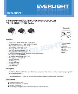
4. Pin Configuration and Schematic
The devices use a standard 6-pin DIP configuration. The pinout is as follows:
- Pin 1: Anode of the input LED.
- Pin 2: Cathode of the input LED.
- Pin 3: No Connection (NC).
- Pin 4: Emitter of the output photodarlington transistor.
- Pin 5: Collector of the output photodarlington transistor.
- Pin 6: Base of the output photodarlington transistor (typically left open or connected for speed-up networks).
The internal schematic shows the infrared LED connected between pins 1 and 2, and the photodarlington transistor connected between pins 4 (Emitter), 5 (Collector), and 6 (Base).
5. Absolute Maximum Ratings
Stresses beyond these limits may cause permanent damage to the device. All ratings are specified at an ambient temperature (Ta) of 25°C unless otherwise noted.
- Input (LED): Forward Current (IF): 60 mA; Peak Forward Current (IFP, 1µs pulse): 1 A; Reverse Voltage (VR): 6 V; Power Dissipation (PD): 120 mW (derating required above Ta = 100°C at 3.8 mW/°C).
- Output (Transistor): Power Dissipation (PC): 150 mW (derating required above Ta = 80°C at 6.5 mW/°C); Collector-Emitter Voltage (VCEO): 55 V; Collector-Base Voltage (VCBO): 55 V; Emitter-Collector Voltage (VECO): 7 V; Emitter-Base Voltage (VEBO): 7 V.
- Device Total: Total Power Dissipation (PTOT): 200 mW; Isolation Voltage (VISO): 5000 Vrms (AC for 1 minute, 40-60% RH).
- Temperature: Operating Temperature (TOPR): -55°C to +100°C; Storage Temperature (TSTG): -55°C to +125°C; Soldering Temperature (TSOL): 260°C (for 10 seconds).
6. Electro-Optical Characteristics
These parameters define the electrical and optical performance under normal operating conditions, typically at Ta=25°C.
6.1 Input Characteristics (LED)
- Forward Voltage (VF): Typically 1.2V, Maximum 1.5V at IF = 10mA (50mA for H11B3).
- Reverse Current (IR): Maximum 10 µA at VR = 6V.
- Input Capacitance (Cin): Typically 50 pF at V=0, f=1MHz.
6.2 Output Characteristics (Photodarlington)
- Collector-Emitter Dark Current (ICEO): Maximum 100 nA at VCE = 10V.
- Collector-Emitter Breakdown Voltage (BVCEO): Minimum 55 V at IC=1mA.
- Collector-Base Breakdown Voltage (BVCBO): Minimum 55 V at IC=0.1mA.
- Emitter-Collector Breakdown Voltage (BVECO): Minimum 7 V at IE=0.1mA.
6.3 Transfer Characteristics
These parameters define the coupling efficiency and switching performance.
- Current Transfer Ratio (CTR): This is the ratio of output collector current to input LED forward current, expressed as a percentage. It varies by part number:
- 4N32, 4N33, H11B1: CTR ≥ 500% (at IF=10mA, VCE=10V or IF=1mA, VCE=5V).
- 4N29, 4N30: CTR ≥ 100%.
- 4N31, H11B3, H11B255: CTR ≥ 100%.
- H11B2: CTR ≥ 200%.
- TIL113: CTR ≥ 300% (at IF=10mA, VCE=1V).
- Collector-Emitter Saturation Voltage (VCE(sat)): Maximum 1.0V to 1.2V depending on the series, under specified IF and IC conditions.
- Isolation Resistance (RIO): Minimum 1011 Ω at VIO=500V DC.
- Input-Output Capacitance (CIO): Typically 0.8 pF at VIO=0, f=1MHz.
- Switching Times: Turn-on time (ton) and turn-off time (toff) are specified for different series under specific test conditions (VCC=10V, with specified IF and load resistor RL=100Ω). For example, H11Bx series ton is typically 25µs and toff is typically 18µs. The 4Nxx and TIL113 series have faster turn-on (max 5µs) but potentially slower turn-off (up to 100µs for some variants).
7. Performance Curves and Switching Characteristics
The datasheet includes typical performance curves (though not detailed in the provided text). These curves typically illustrate the relationship between CTR and temperature, forward current, or collector current. They are essential for designers to understand performance deviations under non-standard conditions. A switching time test circuit is defined, showing the input pulse driving the LED and the resulting output pulse at the collector. Key timing parameters like rise time (tr), fall time (tf), turn-on delay (ton), and turn-off delay (toff) are measured between the 10% and 90% points of the respective pulses.
8. Mechanical and Package Information
The devices are offered in several package variants to suit different assembly processes.
- Standard DIP Type: The classic through-hole package.
- Option M Type: Features a wide lead bend, providing a 0.4-inch (approx. 10.16mm) lead spacing for applications requiring greater creepage distance or easier manual insertion.
- Option S Type: Surface-mount lead form for reflow soldering.
- Option S1 Type: A low-profile surface-mount lead form variant.
Detailed dimensioned drawings are provided for each package type, including body length, width, height, lead pitch, and lead dimensions. A recommended pad layout for the surface-mount options is also included to ensure reliable solder joint formation during PCB assembly.
9. Soldering and Assembly Guidelines
The absolute maximum rating specifies a soldering temperature of 260°C for 10 seconds. This is a critical parameter for reflow or wave soldering processes. Designers must ensure that the thermal profile during assembly does not exceed this limit to prevent damage to the internal semiconductor die or the plastic package. For the surface-mount variants, following the recommended pad layout is crucial to prevent tombstoning or poor solder joints. Proper storage conditions, as per the storage temperature rating (-55°C to +125°C), should be maintained to preserve device integrity before use.
10. Packaging and Ordering Information
The part numbering system is structured to indicate the series, specific part number, lead form option, tape & reel option, and optional safety certification.
Part Number Format: [Series][PartNo][LeadForm][TapeReel]-[Safety]
- Series: 4NXX, H11BX, or TIL113.
- PartNo: For 4NXX: 29,30,31,32,33. For H11BX: 1,2,3,255.
- LeadForm (Y): S (SMD), S1 (Low-profile SMD), M (Wide lead), or none (Standard DIP).
- TapeReel (Z): TA, TB (for SMD options), or none.
- Safety (V): Optional VDE certification.
Packing Quantities:
- Standard DIP and M options: 65 units per tube.
- S and S1 options with TA/TB: 1000 units per reel.
11. Application Design Considerations
When designing with these photodarlington photocouplers, several factors must be considered. The high CTR allows the output transistor to be driven into saturation with relatively low LED current, which is beneficial for interfacing with microcontrollers. However, the photodarlington structure inherently has slower switching speeds compared to phototransistor or photo-IC couplers, making them more suitable for lower-frequency applications (typically up to the tens of kHz range depending on load conditions). The base pin (Pin 6) can be used to connect an external resistor to shunt some of the photogenerated base current to ground, which can significantly improve turn-off time at the expense of reduced CTR. The designer must ensure that the output transistor's voltage ratings (VCEO, VCBO) are not exceeded by the load circuit. A current-limiting resistor is always required in series with the input LED. The value is calculated based on the supply voltage, desired IF, and the LED's VF.
12. Technical Comparison and Selection Guidance
The primary differentiation within this series is the Current Transfer Ratio (CTR). Parts like the 4N32/33 and H11B1 offer very high sensitivity (CTR ≥ 500%), making them ideal for applications where the driving signal is very weak. The 4N29/30 and H11B2 offer medium sensitivity. The 4N31, H11B3, and H11B255 provide a standard 100% CTR. The TIL113 offers a good balance at 300%. The choice between DIP and SMD packages depends on the manufacturing process. The wide-lead (M) option is beneficial for high-voltage applications requiring increased creepage distance on the PCB. Compared to simpler phototransistor couplers, photodarlingtons provide much higher gain but are slower. For very high-speed digital isolation, other technologies like digital isolators or faster optocouplers with logic-gate outputs would be more appropriate.
13. Frequently Asked Questions (FAQ)
Q: What is the main advantage of a photodarlington over a standard phototransistor?
A: The primary advantage is a much higher current transfer ratio (CTR), often by a factor of 10 to 100. This means a very small input LED current can control a much larger output current, simplifying drive circuitry.
Q: Why are the switching times slower for photodarlingtons?
A: The darlington pair configuration has an extra transistor stage, which increases charge storage and reduces switching speed, particularly during turn-off.
Q: How can I improve the turn-off time of the photodarlington?
A: Connecting an external resistor (typically in the range of 10kΩ to 100kΩ) between the base pin (6) and the emitter pin (4) will provide a path to bleed off stored charge, significantly reducing turn-off time.
Q: What does the 5000 Vrms isolation rating mean for my design?
A: This rating certifies that the device can withstand a 5000 Volt AC potential difference between the input and output sides for one minute without breakdown. It defines the safety barrier for your system, protecting users and low-voltage circuitry from high-voltage faults.
Q: Can I use these for AC input signals?
A: The input is an LED, which is a diode. It will only conduct during the positive half-cycle of an AC signal. For true AC input sensing, a bridge rectifier or a dedicated AC-input optocoupler is required.
14. Design and Usage Examples
Example 1: Microcontroller Relay Driver: A common use is to isolate a 3.3V or 5V microcontroller from a 12V or 24V relay coil. The microcontroller GPIO pin, through a current-limiting resistor (e.g., 220Ω for 5V supply and ~10mA IF), drives the LED side. The photodarlington's collector is connected to the relay coil, and the emitter to ground. A flyback diode must be placed across the relay coil. The high CTR ensures the relay is fully energized even if the microcontroller pin can only source a modest current.
Example 2: Mains Voltage Zero-Crossing Detection: While not for direct mains connection, these couplers can be used in the isolated feedback path of a switched-mode power supply or in a zero-crossing detection circuit where a higher-voltage, isolated signal needs to be communicated to a low-voltage logic circuit. The high isolation voltage is critical here.
Example 3: Industrial Digital Input Module: In a PLC input module, these optocouplers can isolate field sensor signals (e.g., 24V DC proximity switches) from the internal logic circuitry, providing noise immunity and protecting the central controller from voltage transients on the field side.
15. Operating Principle
The fundamental principle is electro-optical-electrical conversion. When a forward current (IF) is applied to the input infrared LED, it emits photons (light). This light travels across a transparent insulating gap within the package and strikes the base region of the output silicon photodarlington transistor. The absorbed photons generate electron-hole pairs, creating a photocurrent that acts as the base current for the first transistor of the darlington pair. This small photocurrent is amplified by the high gain of the two transistors, resulting in a much larger collector current (IC) that can switch an external load. The key is that the only connection between the input and output is the beam of light, providing the electrical isolation.
16. Technology Trends
Photodarlington optocouplers represent a mature and well-established technology. While they continue to be widely used for their simplicity, high gain, and cost-effectiveness in many isolation applications, several trends are notable. There is a general industry shift towards surface-mount packages (like the S and S1 options) to enable automated assembly and reduce board space. The demand for higher data rates in industrial communications is driving adoption of faster technologies like digital isolators (based on capacitive or magnetic coupling) and high-speed optocouplers with integrated logic. However, for applications prioritizing high isolation voltage, robustness, and high current drive capability at lower frequencies, photodarlington couplers remain a highly relevant and reliable solution. Ongoing developments focus on improving the high-temperature performance and long-term reliability of the LED and plastic encapsulant materials.
LED Specification Terminology
Complete explanation of LED technical terms
Photoelectric Performance
| Term | Unit/Representation | Simple Explanation | Why Important |
|---|---|---|---|
| Luminous Efficacy | lm/W (lumens per watt) | Light output per watt of electricity, higher means more energy efficient. | Directly determines energy efficiency grade and electricity cost. |
| Luminous Flux | lm (lumens) | Total light emitted by source, commonly called "brightness". | Determines if the light is bright enough. |
| Viewing Angle | ° (degrees), e.g., 120° | Angle where light intensity drops to half, determines beam width. | Affects illumination range and uniformity. |
| CCT (Color Temperature) | K (Kelvin), e.g., 2700K/6500K | Warmth/coolness of light, lower values yellowish/warm, higher whitish/cool. | Determines lighting atmosphere and suitable scenarios. |
| CRI / Ra | Unitless, 0–100 | Ability to render object colors accurately, Ra≥80 is good. | Affects color authenticity, used in high-demand places like malls, museums. |
| SDCM | MacAdam ellipse steps, e.g., "5-step" | Color consistency metric, smaller steps mean more consistent color. | Ensures uniform color across same batch of LEDs. |
| Dominant Wavelength | nm (nanometers), e.g., 620nm (red) | Wavelength corresponding to color of colored LEDs. | Determines hue of red, yellow, green monochrome LEDs. |
| Spectral Distribution | Wavelength vs intensity curve | Shows intensity distribution across wavelengths. | Affects color rendering and quality. |
Electrical Parameters
| Term | Symbol | Simple Explanation | Design Considerations |
|---|---|---|---|
| Forward Voltage | Vf | Minimum voltage to turn on LED, like "starting threshold". | Driver voltage must be ≥Vf, voltages add up for series LEDs. |
| Forward Current | If | Current value for normal LED operation. | Usually constant current drive, current determines brightness & lifespan. |
| Max Pulse Current | Ifp | Peak current tolerable for short periods, used for dimming or flashing. | Pulse width & duty cycle must be strictly controlled to avoid damage. |
| Reverse Voltage | Vr | Max reverse voltage LED can withstand, beyond may cause breakdown. | Circuit must prevent reverse connection or voltage spikes. |
| Thermal Resistance | Rth (°C/W) | Resistance to heat transfer from chip to solder, lower is better. | High thermal resistance requires stronger heat dissipation. |
| ESD Immunity | V (HBM), e.g., 1000V | Ability to withstand electrostatic discharge, higher means less vulnerable. | Anti-static measures needed in production, especially for sensitive LEDs. |
Thermal Management & Reliability
| Term | Key Metric | Simple Explanation | Impact |
|---|---|---|---|
| Junction Temperature | Tj (°C) | Actual operating temperature inside LED chip. | Every 10°C reduction may double lifespan; too high causes light decay, color shift. |
| Lumen Depreciation | L70 / L80 (hours) | Time for brightness to drop to 70% or 80% of initial. | Directly defines LED "service life". |
| Lumen Maintenance | % (e.g., 70%) | Percentage of brightness retained after time. | Indicates brightness retention over long-term use. |
| Color Shift | Δu′v′ or MacAdam ellipse | Degree of color change during use. | Affects color consistency in lighting scenes. |
| Thermal Aging | Material degradation | Deterioration due to long-term high temperature. | May cause brightness drop, color change, or open-circuit failure. |
Packaging & Materials
| Term | Common Types | Simple Explanation | Features & Applications |
|---|---|---|---|
| Package Type | EMC, PPA, Ceramic | Housing material protecting chip, providing optical/thermal interface. | EMC: good heat resistance, low cost; Ceramic: better heat dissipation, longer life. |
| Chip Structure | Front, Flip Chip | Chip electrode arrangement. | Flip chip: better heat dissipation, higher efficacy, for high-power. |
| Phosphor Coating | YAG, Silicate, Nitride | Covers blue chip, converts some to yellow/red, mixes to white. | Different phosphors affect efficacy, CCT, and CRI. |
| Lens/Optics | Flat, Microlens, TIR | Optical structure on surface controlling light distribution. | Determines viewing angle and light distribution curve. |
Quality Control & Binning
| Term | Binning Content | Simple Explanation | Purpose |
|---|---|---|---|
| Luminous Flux Bin | Code e.g., 2G, 2H | Grouped by brightness, each group has min/max lumen values. | Ensures uniform brightness in same batch. |
| Voltage Bin | Code e.g., 6W, 6X | Grouped by forward voltage range. | Facilitates driver matching, improves system efficiency. |
| Color Bin | 5-step MacAdam ellipse | Grouped by color coordinates, ensuring tight range. | Guarantees color consistency, avoids uneven color within fixture. |
| CCT Bin | 2700K, 3000K etc. | Grouped by CCT, each has corresponding coordinate range. | Meets different scene CCT requirements. |
Testing & Certification
| Term | Standard/Test | Simple Explanation | Significance |
|---|---|---|---|
| LM-80 | Lumen maintenance test | Long-term lighting at constant temperature, recording brightness decay. | Used to estimate LED life (with TM-21). |
| TM-21 | Life estimation standard | Estimates life under actual conditions based on LM-80 data. | Provides scientific life prediction. |
| IESNA | Illuminating Engineering Society | Covers optical, electrical, thermal test methods. | Industry-recognized test basis. |
| RoHS / REACH | Environmental certification | Ensures no harmful substances (lead, mercury). | Market access requirement internationally. |
| ENERGY STAR / DLC | Energy efficiency certification | Energy efficiency and performance certification for lighting. | Used in government procurement, subsidy programs, enhances competitiveness. |