1. Product Overview
The H11AAX series represents a family of AC input photocouplers, also known as optocouplers or opto-isolators. These devices are specifically engineered to provide galvanic isolation between an AC or unknown-polarity DC input circuit and an output control circuit. The core function is to transfer electrical signals using light, thereby eliminating electrical connections and preventing ground loops, voltage spikes, and noise from propagating between circuits.
The series includes four main variants: H11AA1, H11AA2, H11AA3, and H11AA4. The primary differentiating factor among them is the Current Transfer Ratio (CTR), which defines the efficiency of signal transfer from the input to the output. These devices are housed in a compact 6-pin Dual In-line Package (DIP), with options for standard through-hole mounting, wide lead spacing, and surface-mount technology (SMD).
1.1 Core Advantages and Target Market
The H11AAX series offers several key advantages that make it suitable for demanding industrial and consumer applications. Its most prominent feature is the high isolation voltage of 5000Vrms, which is critical for safety and reliability in mains-connected equipment. A creepage distance exceeding 7.62mm further enhances this safety rating. The devices have received approvals from major international safety agencies including UL, cUL, VDE, SEMKO, NEMKO, DEMKO, FIMKO, and CQC, making them globally acceptable for products requiring regulatory compliance.
The integrated inverse-parallel infrared LED configuration on the input side is a defining characteristic. This design allows the device to be driven directly by an AC voltage or a DC voltage of unknown polarity, simplifying circuit design by eliminating the need for external rectification circuitry. The output is a silicon NPN phototransistor.
The target markets and applications are diverse, primarily focusing on areas where electrical isolation and AC signal sensing are paramount. Typical applications include AC line monitoring for detecting the presence or absence of mains voltage, telephone line interface circuits, and sensors for detecting unknown polarity DC signals in industrial control systems.
2. Technical Parameter Deep-Dive
This section provides a detailed, objective analysis of the electrical, optical, and thermal characteristics specified in the datasheet. Understanding these parameters is crucial for reliable circuit design.
2.1 Absolute Maximum Ratings
These ratings define the stress limits beyond which permanent damage to the device may occur. Operation under these conditions is not guaranteed.
- Input Forward Current (IF): 60 mA (continuous). This is the maximum DC current that can be applied to the input LEDs.
- Peak Forward Current (IFM): 1 A for a very short pulse duration of 10 µs. This rating is important for withstanding transient surges.
- Input Power Dissipation (PD): 120 mW at 25°C ambient, derating at 3.8 mW/°C above 90°C. This limits the combined VF * IF product.
- Output Collector-Emitter Voltage (VCEO): 80 V. The maximum voltage that can be sustained across the phototransistor's collector and emitter when the base is open.
- Total Device Power Dissipation (PTOT): 200 mW. The sum of input and output power should not exceed this value.
- Isolation Voltage (VISO): 5000 Vrms for 1 minute at 40-60% relative humidity. This is a key safety parameter tested with input and output pins shorted separately.
- Operating Temperature (TOPR): -55°C to +100°C. The device is functional within this full industrial temperature range.
- Soldering Temperature (TSOL): 260°C for 10 seconds, relevant for wave or reflow soldering processes.
2.2 Electro-Optical Characteristics
These parameters are typically measured at 25°C and define the device's performance under normal operating conditions.
2.2.1 Input Characteristics
- Forward Voltage (VF): Typically 1.2V, with a maximum of 1.5V at a forward current (IF) of ±10mA. The symmetrical value indicates the behavior of the inverse-parallel LED pair.
- Input Capacitance (Cin): Typically 80 pF. This can affect high-frequency performance of the driving circuit.
2.2.2 Output Characteristics
- Collector-Emitter Dark Current (ICEO): Maximum 50 nA at VCE=10V and IF=0mA. This is the leakage current of the phototransistor when no light is incident, important for off-state leakage.
- Breakdown Voltages (BVCEO, BVCBO, BVECO): Minimum 80V, 80V, and 7V respectively. These define the voltage withstand capability under different pin configurations.
- Collector-Emitter Saturation Voltage (VCE(sat)): Maximum 0.4V at IF=±10mA and IC=0.5mA. This is the voltage drop across the output transistor when it is fully turned on.
2.2.3 Transfer Characteristics
These parameters define the signal transfer efficiency and speed.
- Current Transfer Ratio (CTR): This is the core grading parameter for the series, defined as (IC / IF) * 100% under specified conditions (IF=±10mA, VCE=10V).
- H11AA1: CTR ≥ 20%
- H11AA2: CTR ≥ 10%
- H11AA3: CTR ≥ 50%
- H11AA4: CTR ≥ 100%
- CTR Symmetry: Ratio of CTR for one LED polarity to the other, specified between 0.5 and 2.0. This indicates how balanced the two inverse-parallel LEDs are.
- Isolation Resistance (RIO): Minimum 10^11 Ω at 500V DC. This is the DC resistance between the input and output, contributing to the isolation quality.
- Input-Output Capacitance (CIO): Typically 0.7 pF. This very low capacitance is crucial for rejecting high-frequency common-mode noise across the isolation barrier.
- Switching Times (Ton, Toff, Tr, Tf): All have a maximum value of 10 µs under the test condition (VCC=10V, IC=10mA, RL=100Ω). These times define how quickly the output can respond to changes in the input signal, limiting the maximum AC frequency or data rate.
3. Grading System Explanation
The H11AAX series employs a straightforward grading system based solely on the Current Transfer Ratio (CTR).
CTR Grading (X in H11AAX): The numerical suffix (1, 2, 3, 4) directly corresponds to the minimum guaranteed CTR percentage as listed in section 2.2.3. There is no grading based on wavelength, forward voltage, or other parameters. Designers must select the appropriate grade based on the required output current drive capability versus the available input current. For example, the H11AA4 (100% min CTR) is the most sensitive and would be chosen for applications where the input drive capability is very low, while the H11AA2 might be sufficient and more cost-effective in circuits with higher available drive current.
4. Performance Curve Analysis
The datasheet references typical electro-optical characteristic curves. While the specific graphs are not reproduced in the provided text, their purpose and the information they convey are standard for such components.
Typical Curves would include:
- Current Transfer Ratio (CTR) vs. Forward Current (IF): This curve shows how the CTR varies with the driving current. Typically, CTR is highest at a moderate IF and may decrease at very low or very high currents.
- CTR vs. Ambient Temperature (Ta): Photocoupler CTR generally has a negative temperature coefficient, meaning it decreases as temperature increases. This graph is critical for designing circuits that operate over the full temperature range.
- Collector Current (IC) vs. Collector-Emitter Voltage (VCE): This is the output characteristic family of curves, similar to a bipolar transistor, with input LED current (IF) as the parameter. It shows the saturation region and the active region.
- Forward Voltage (VF) vs. Forward Current (IF): The IV characteristic of the input LED pair.
- Switching Time vs. Load Resistance (RL): Shows how the rise, fall, turn-on, and turn-off times are affected by the output load.
Designers should consult these curves in the full datasheet to understand non-linear behaviors and derating factors not captured by the table of minimum/typical/maximum values.
5. Mechanical and Package Information
The device is offered in several package variants to suit different assembly processes.
5.1 Package Dimensions and Types
- Standard DIP Type: The default through-hole package.
- Option M Type: Features a \"wide lead bend\" providing a 0.4-inch (approx. 10.16mm) lead spacing instead of the standard 0.3-inch (7.62mm), useful for boards requiring greater creepage distance.
- Option S Type: Surface-mount lead form for reflow soldering.
- Option S1 Type: A \"low profile\" surface-mount version, likely with a lower standoff height from the PCB.
Detailed dimensioned drawings are provided for each type, including body size, lead length, lead spacing, and coplanarity specifications. These are essential for PCB footprint design.
5.2 Pad Layout and Polarity Identification
A recommended pad layout for the surface-mount options (S and S1) is provided. The datasheet notes that this is a suggestion and designers should modify it based on their specific PCB manufacturing process and thermal requirements.
Device Marking: The top of the package is marked with:
- \"EL\" (manufacturer code)
- The full part number (e.g., H11AA1)
- A 1-digit year code (Y)
- A 2-digit week code (WW)
- An optional \"V\" suffix if VDE safety approval is specified for that unit.
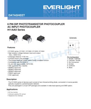
Pin Configuration (6-Pin DIP):
1. Anode / Cathode (LED1 Anode, LED2 Cathode)
2. Cathode / Anode (LED1 Cathode, LED2 Anode)
3. No Connection (NC)
4. Emitter (of Phototransistor)
5. Collector (of Phototransistor)
6. Base (of Phototransistor). The base pin is typically left open or connected to the emitter via a resistor for sensitivity adjustment or speed improvement.
6. Soldering and Assembly Guidelines
The key guideline from the Absolute Maximum Ratings is the soldering temperature: 260°C for a maximum of 10 seconds. This is compatible with standard lead-free (SnAgCu) reflow profiles.
Important Considerations:
- Moisture Sensitivity: While not explicitly stated in the provided text, plastic encapsulated SMD optocouplers often have a Moisture Sensitivity Level (MSL). For surface-mount parts (Options S, S1), it is critical to follow the manufacturer's handling instructions regarding baking and floor life to prevent \"popcorning\" during reflow.
- Cleaning: Ensure cleaning solvents are compatible with the device's plastic material.
- Storage Conditions: As per the datasheet, the storage temperature range is -55°C to +125°C. Devices should be stored in a dry, anti-static environment.
7. Packaging and Ordering Information
The ordering code follows the pattern: H11AAXY(Z)-V
- X: CTR Rank (1, 2, 3, 4).
- Y: Lead Form Option.
- None: Standard DIP-6 (65 units/tube).
- M: Wide lead bend (65 units/tube).
- S: Surface mount lead form.
- S1: Low profile surface mount lead form.
- Z: Tape and Reel Option (for S/S1 only).
- TA: Specific tape and reel type.
- TB: Alternative tape and reel type.
- Both TA and TB pack 1000 units per reel.
- V: Optional VDE safety approval marking.
Tape and Reel Specifications: Detailed dimensions for the carrier tape (pocket size A, B), cover tape, and reel are provided for automated pick-and-place assembly.
8. Application Suggestions
8.1 Typical Application Circuits
AC Line Monitor: The input is connected directly across the AC line (with a current-limiting resistor). The output transistor switches in sync with the AC zero-crossings, providing a digital pulse train or a rectified signal to a microcontroller for detecting power presence.
Unknown Polarity DC Sensor: The inverse-parallel input allows the device to be connected to a DC voltage source without regard to polarity, making it ideal for sensing in battery-powered equipment or industrial sensors where wiring polarity might be reversed.
Telephone Line Interface: Used for ring detection or off-hook detection, providing isolation between the telephone line and the logic circuitry.
8.2 Design Considerations
- Input Current Limiting: A series resistor must always be used to limit the input current (IF) to a safe value below 60mA, calculated based on the peak input voltage and the LED forward voltage.
- Output Loading: The load resistor (RL) on the collector determines the output voltage swing and affects switching speed. A smaller RL gives faster switching but consumes more power.
- Noise Immunity: The low input-output capacitance (0.7pF) provides excellent rejection of high-frequency common-mode noise. For best performance, keep the input and output traces physically separated on the PCB.
- CTR Degradation: Over very long periods and at high temperatures, the CTR of photocouplers can degrade. For critical long-life applications, design with substantial initial CTR margin.
9. Technical Comparison and Differentiation
The H11AAX series differentiates itself primarily through its AC input capability via the inverse-parallel LED structure. Most standard photocouplers (e.g., 4N25, PC817) have a single LED input requiring a defined forward bias, necessitating an external bridge rectifier for AC operation. The H11AAX integrates this functionality.
Compared to other AC input photocouplers, its key advantages are the high 5000Vrms isolation rating and the comprehensive suite of international safety approvals (UL, VDE, etc.), which are essential for products sold in multiple global markets. The availability of multiple CTR grades and package types (through-hole and SMD) provides design flexibility.
10. Frequently Asked Questions (Based on Technical Parameters)
Q1: Can I drive the H11AAX directly from 120VAC or 230VAC mains?
A: Not directly. You must use a current-limiting resistor in series with the input. The resistor value must be calculated based on the peak mains voltage (e.g., ~340V for 230VAC), the desired forward current, and the LED's VF. The resistor's power rating must also be considered.
Q2: What is the maximum AC frequency I can use with this photocoupler?
A: The maximum switching time is 10 µs. This theoretically allows a square wave frequency up to about 50 kHz. However, for a clean 50/60 Hz AC sine wave sensing, it is perfectly suitable as the period (16.7ms/20ms) is much longer than the switching time.
Q3: Why is there a Base pin (Pin 6), and how should I use it?
A: The base pin provides access to the phototransistor's base. Leaving it open is standard. Connecting a resistor between base and emitter can:
1. Improve Speed: A low-value resistor (e.g., 10kΩ to 100kΩ) shunts stored charge, reducing turn-off time (Toff).
2. Reduce Sensitivity/Increase Threshold: A resistor provides a leakage path, slightly increasing the minimum input current required to turn on the output.
Q4: How do I choose between the different CTR grades (H11AA1, AA2, AA3, AA4)?
A: Choose based on your input drive capability and required output current. If your circuit can only provide a small input current (e.g., from a high-voltage resistor), choose a higher CTR grade (AA3 or AA4) to get sufficient output. If input current is plentiful, a lower grade (AA1 or AA2) may be more cost-effective. Always design with margin for CTR degradation over time and temperature.
11. Practical Design Case Study
Scenario: Designing a 230VAC Mains Presence Detector.
Goal: Provide a 3.3V logic-high signal to a microcontroller when 230VAC is present.
Design Steps:
1. Part Selection: H11AA1 (20% CTR minimum) is chosen as the input current will be sufficient.
2. Input Resistor Calculation: Peak voltage = 230V * √2 ≈ 325V. Desired IF ≈ 10mA (for good CTR). VF ≈ 1.2V. R = (325V - 1.2V) / 0.01A ≈ 32.4kΩ. Use a standard 33kΩ resistor. Power dissipation in R: P = (230V)^2 / 33000Ω ≈ 1.6W. A 2W or 3W rated resistor is required.
3. Output Circuit: Connect the collector (Pin 5) to the 3.3V microcontroller supply via a pull-up resistor (e.g., 10kΩ). Connect the emitter (Pin 4) to ground. The base (Pin 6) is left open.
4. Operation: When AC is present, the output transistor turns on during each half-cycle, pulling the collector (and the MCU input pin) low. The MCU sees a 50/60 Hz pulsating low signal, which can be debounced in software to indicate \"power on.\"
5. PCB Layout: Maintain >7.62mm creepage distance between the input-side (pins 1,2,3, resistor) and output-side (pins 4,5,6, MCU) traces on the PCB to preserve the isolation rating.
12. Operating Principle
The H11AAX operates on the principle of opto-electronic isolation. On the input side, two gallium arsenide infrared light-emitting diodes (LEDs) are connected in inverse parallel. When an AC voltage is applied (with a series current-limiting resistor), one LED conducts and emits light during the positive half-cycle, and the other LED conducts and emits light during the negative half-cycle. Thus, infrared light pulses are generated at twice the frequency of the input AC signal.
This light travels across a transparent isolation barrier within the package. On the output side, the light falls on the base region of a silicon NPN phototransistor. The photons generate electron-hole pairs, creating a base current that turns on the transistor, allowing a collector current (IC) to flow. The ratio of this output collector current to the input forward current is the Current Transfer Ratio (CTR). The phototransistor's collector-emitter voltage is controlled by the external load circuit.
13. Technology Trends
Photocoupler technology continues to evolve. While the fundamental principle remains, trends include:
- Higher Speed: Development of devices with faster switching times (nanoseconds) for digital communication and inverter gate drive applications, often using photodiode or IC-based outputs instead of phototransistors.
- Higher Integration: Combining the photocoupler with additional functions like IGBT gate drivers, error amplifiers, or digital interfaces (I²C isolators).
- Improved Reliability and Lifetime: Advancements in LED materials and packaging to reduce the rate of CTR degradation over time and temperature.
- Miniaturization: Continued reduction in package size, especially for surface-mount versions, to save PCB space.
- Alternative Isolation Technologies: Capacitive and magnetic (giant magnetoresistance, GMR) isolators compete in some high-speed, high-density applications, though optocouplers retain advantages in high common-mode transient immunity (CMTI) and well-established safety certifications.
The H11AAX series, with its robust design and safety approvals, represents a mature and reliable solution for traditional AC sensing and basic isolation needs, where its integrated AC input capability provides a distinct advantage.
LED Specification Terminology
Complete explanation of LED technical terms
Photoelectric Performance
| Term | Unit/Representation | Simple Explanation | Why Important |
|---|---|---|---|
| Luminous Efficacy | lm/W (lumens per watt) | Light output per watt of electricity, higher means more energy efficient. | Directly determines energy efficiency grade and electricity cost. |
| Luminous Flux | lm (lumens) | Total light emitted by source, commonly called "brightness". | Determines if the light is bright enough. |
| Viewing Angle | ° (degrees), e.g., 120° | Angle where light intensity drops to half, determines beam width. | Affects illumination range and uniformity. |
| CCT (Color Temperature) | K (Kelvin), e.g., 2700K/6500K | Warmth/coolness of light, lower values yellowish/warm, higher whitish/cool. | Determines lighting atmosphere and suitable scenarios. |
| CRI / Ra | Unitless, 0–100 | Ability to render object colors accurately, Ra≥80 is good. | Affects color authenticity, used in high-demand places like malls, museums. |
| SDCM | MacAdam ellipse steps, e.g., "5-step" | Color consistency metric, smaller steps mean more consistent color. | Ensures uniform color across same batch of LEDs. |
| Dominant Wavelength | nm (nanometers), e.g., 620nm (red) | Wavelength corresponding to color of colored LEDs. | Determines hue of red, yellow, green monochrome LEDs. |
| Spectral Distribution | Wavelength vs intensity curve | Shows intensity distribution across wavelengths. | Affects color rendering and quality. |
Electrical Parameters
| Term | Symbol | Simple Explanation | Design Considerations |
|---|---|---|---|
| Forward Voltage | Vf | Minimum voltage to turn on LED, like "starting threshold". | Driver voltage must be ≥Vf, voltages add up for series LEDs. |
| Forward Current | If | Current value for normal LED operation. | Usually constant current drive, current determines brightness & lifespan. |
| Max Pulse Current | Ifp | Peak current tolerable for short periods, used for dimming or flashing. | Pulse width & duty cycle must be strictly controlled to avoid damage. |
| Reverse Voltage | Vr | Max reverse voltage LED can withstand, beyond may cause breakdown. | Circuit must prevent reverse connection or voltage spikes. |
| Thermal Resistance | Rth (°C/W) | Resistance to heat transfer from chip to solder, lower is better. | High thermal resistance requires stronger heat dissipation. |
| ESD Immunity | V (HBM), e.g., 1000V | Ability to withstand electrostatic discharge, higher means less vulnerable. | Anti-static measures needed in production, especially for sensitive LEDs. |
Thermal Management & Reliability
| Term | Key Metric | Simple Explanation | Impact |
|---|---|---|---|
| Junction Temperature | Tj (°C) | Actual operating temperature inside LED chip. | Every 10°C reduction may double lifespan; too high causes light decay, color shift. |
| Lumen Depreciation | L70 / L80 (hours) | Time for brightness to drop to 70% or 80% of initial. | Directly defines LED "service life". |
| Lumen Maintenance | % (e.g., 70%) | Percentage of brightness retained after time. | Indicates brightness retention over long-term use. |
| Color Shift | Δu′v′ or MacAdam ellipse | Degree of color change during use. | Affects color consistency in lighting scenes. |
| Thermal Aging | Material degradation | Deterioration due to long-term high temperature. | May cause brightness drop, color change, or open-circuit failure. |
Packaging & Materials
| Term | Common Types | Simple Explanation | Features & Applications |
|---|---|---|---|
| Package Type | EMC, PPA, Ceramic | Housing material protecting chip, providing optical/thermal interface. | EMC: good heat resistance, low cost; Ceramic: better heat dissipation, longer life. |
| Chip Structure | Front, Flip Chip | Chip electrode arrangement. | Flip chip: better heat dissipation, higher efficacy, for high-power. |
| Phosphor Coating | YAG, Silicate, Nitride | Covers blue chip, converts some to yellow/red, mixes to white. | Different phosphors affect efficacy, CCT, and CRI. |
| Lens/Optics | Flat, Microlens, TIR | Optical structure on surface controlling light distribution. | Determines viewing angle and light distribution curve. |
Quality Control & Binning
| Term | Binning Content | Simple Explanation | Purpose |
|---|---|---|---|
| Luminous Flux Bin | Code e.g., 2G, 2H | Grouped by brightness, each group has min/max lumen values. | Ensures uniform brightness in same batch. |
| Voltage Bin | Code e.g., 6W, 6X | Grouped by forward voltage range. | Facilitates driver matching, improves system efficiency. |
| Color Bin | 5-step MacAdam ellipse | Grouped by color coordinates, ensuring tight range. | Guarantees color consistency, avoids uneven color within fixture. |
| CCT Bin | 2700K, 3000K etc. | Grouped by CCT, each has corresponding coordinate range. | Meets different scene CCT requirements. |
Testing & Certification
| Term | Standard/Test | Simple Explanation | Significance |
|---|---|---|---|
| LM-80 | Lumen maintenance test | Long-term lighting at constant temperature, recording brightness decay. | Used to estimate LED life (with TM-21). |
| TM-21 | Life estimation standard | Estimates life under actual conditions based on LM-80 data. | Provides scientific life prediction. |
| IESNA | Illuminating Engineering Society | Covers optical, electrical, thermal test methods. | Industry-recognized test basis. |
| RoHS / REACH | Environmental certification | Ensures no harmful substances (lead, mercury). | Market access requirement internationally. |
| ENERGY STAR / DLC | Energy efficiency certification | Energy efficiency and performance certification for lighting. | Used in government procurement, subsidy programs, enhances competitiveness. |