1. Product Overview
The ELS3120-G Series is a high-performance, 6-pin Single-Dual In-line Package (SDIP) photocoupler specifically engineered for driving the gates of Insulated-Gate Bipolar Transistors (IGBTs) and power Metal-Oxide-Semiconductor Field-Effect Transistors (MOSFETs). It integrates an infrared Light Emitting Diode (LED) optically coupled to a monolithic integrated circuit featuring a robust power output stage. A key design feature is an internal shield that ensures high immunity to common-mode transient noise, making it exceptionally reliable in electrically noisy power conversion environments. The device is characterized by its rail-to-rail output voltage capability, allowing it to fully turn on and off the driven power switch.
1.1 Core Advantages and Target Market
The primary advantage of the ELS3120 lies in its combination of high output current drive capability (2.5A peak) and excellent isolation characteristics (5000Vrms). This makes it an ideal solution for applications requiring safe and robust electrical isolation between low-voltage control circuits and high-voltage power stages. Its guaranteed performance over a wide temperature range from -40°C to +110°C ensures reliability in demanding conditions. The device is compliant with halogen-free requirements (Br < 900 ppm, Cl < 900 ppm, Br+Cl < 1500 ppm), is lead-free, and RoHS compliant. It has received approvals from major international safety standards bodies including UL, cUL, VDE, SEMKO, NEMKO, DEMKO, FIMKO, and CQC. The target market includes industrial motor drives, uninterruptible power supplies (UPS), solar inverters, and various home appliance applications such as fan heaters.
2. In-Depth Technical Parameter Analysis
2.1 Absolute Maximum Ratings
The device is designed to operate within strict limits to ensure longevity and prevent damage. Key absolute maximum ratings include: a continuous forward current (IF) of 25mA for the input LED, with a pulsed forward current (IFP) capability of 1A for very short durations (≤1μs). The reverse voltage (VR) for the LED is limited to 5V. On the output side, the peak output current (IOPH/IOPL) is ±2.5A, and the peak output voltage (VO) relative to VEE must not exceed 30V. The supply voltage (VCC - VEE) can range from 15V to 30V. The device can withstand an isolation voltage (VISO) of 5000Vrms for one minute. The total power dissipation (PT) is 300mW. The operating temperature range (TOPR) is -40°C to +110°C, and storage temperature (TSTG) ranges from -55°C to +125°C. The soldering temperature (TSOL) is rated at 260°C for 10 seconds.
2.2 Electro-Optical Characteristics
This section details the guaranteed performance parameters under specified operating conditions across the temperature range. For the input, the maximum forward voltage (VF) is 1.8V at a forward current (IF) of 10mA. The output characteristics are divided into supply current and transfer characteristics. The high and low level supply currents (ICCH and ICCL) have a typical value of around 1.4-1.5mA and a maximum of 3.2mA when VCC=30V. The transfer characteristics are critical for gate driving. The high-level output current (IOH) is specified as a minimum of -1A (sourcing current) when VCC=30V and the output is 3V below VCC, and -2.5A minimum when the output is 6V below VCC. Conversely, the low-level output current (IOL) is a minimum of 1A (sinking current) when the output is 3V above VEE, and 2.5A minimum when 6V above VEE. The input threshold current (IFLH) to initiate switching is a maximum of 5mA. The device also incorporates Under-Voltage Lockout (UVLO) protection, with thresholds typically around 11-13.5V for VUVLO+ (turn-on) and 10-12.5V for VUVLO- (turn-off), preventing malfunction when the supply voltage is insufficient.
2.3 Switching Characteristics
The dynamic performance is vital for efficient power switching. Key parameters measured under standard conditions (IF=7-16mA, VCC=15-30V, Cg=10nF, Rg=10Ω, f=10kHz) include: propagation delay times (tPLH and tPHL) with a typical value of 150ns and a maximum of 300ns. The output rise and fall times (tR and tF) are typically 80ns. Pulse width distortion, defined as |tPHL – tPLH|, has a maximum of 100ns, indicating good symmetry. Propagation delay skew (tPSK), the variation in delay between multiple units under identical conditions, is a maximum of 150ns. A standout feature is the Common Mode Transient Immunity (CMTI), which is guaranteed to be a minimum of ±25 kV/μs for both high (CMH) and low (CML) output states. This high CMTI rating is crucial for rejecting fast voltage transients across the isolation barrier that could cause erroneous output switching.
3. Performance Curve Analysis
The datasheet provides several typical characteristic curves that offer deeper insight into device behavior under varying conditions. Figure 1 shows how the LED forward voltage (VF) decreases with increasing ambient temperature (TA) for different forward currents, which is important for thermal design of the input circuit. Figure 2 plots the output high voltage drop (VOH - VCC) versus the output high current (IOH) at different temperatures, illustrating the effective on-resistance of the high-side output transistor. Figure 3 shows how this voltage drop changes with temperature at a fixed load current. Similarly, Figure 4 and Figure 5 depict the output low voltage (VOL) versus output low current (IOL) and its variation with temperature, characterizing the low-side sink capability. Figure 6 graphs the supply current (ICCH and ICCL) versus ambient temperature, showing stable quiescent current consumption. Figure 7 (implied from the PDF fragment) likely shows supply current versus supply voltage, indicating the device's power consumption dependency on VCC.
4. Mechanical and Package Information
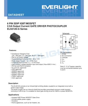
The device is housed in a 6-pin Single/Dual In-line Package (SDIP). The pin configuration is as follows: Pin 1: Anode of the input LED; Pin 2: No Connection (NC); Pin 3: Cathode of the input LED; Pin 4: VEE (Negative output supply/ground); Pin 5: VOUT (Gate drive output); Pin 6: VCC (Positive output supply). A critical application note specifies that a 0.1μF bypass capacitor must be connected between pins 4 (VEE) and 6 (VCC) as close as possible to the device body to ensure stable operation and minimize supply line inductance during high-current switching.
5. Application Guidelines
5.1 Typical Application Circuits
The primary application is as an isolated gate driver for IGBTs and power MOSFETs in bridge configurations (e.g., half-bridge, full-bridge). The photocoupler provides the necessary isolation between the microcontroller or PWM controller (low-voltage side) and the floating gate of the high-side switch (high-voltage side). The 2.5A peak current allows for fast charging and discharging of the power device's gate capacitance, minimizing switching losses.
5.2 Design Considerations
Several factors must be considered for reliable operation. The gate resistor (Rg) value should be chosen based on the required switching speed and to prevent gate ringing or excessive dV/dt. The recommended 0.1μF bypass capacitor between VCC and VEE is mandatory to provide a local low-impedance source for the high peak currents. The UVLO feature protects the power device but must be accounted for in the supply sequencing. The common-mode transient immunity is high, but PCB layout remains critical: the isolation gap between input and output circuits must be maintained, and high dV/dt loops should be kept small and away from sensitive input traces.
6. Technical Comparison and Differentiation
Compared to basic optocouplers or some integrated gate driver ICs without isolation, the ELS3120 offers a dedicated, high-current output stage integrated with an opto-isolator. Its key differentiators are the 2.5A peak output current, which is higher than many standard optocoupler-based drivers, and the guaranteed high CMTI of 25 kV/μs, which is essential for modern fast-switching silicon carbide (SiC) or gallium nitride (GaN) applications. The wide operating temperature range and multitude of international safety approvals make it suitable for industrial and appliance markets where reliability and compliance are paramount.
7. Frequently Asked Questions (FAQ)
Q: What is the purpose of the internal shield?
A: The internal shield significantly enhances the Common Mode Transient Immunity (CMTI) by reducing capacitive coupling between the input and output, preventing false triggering from fast voltage transients across the isolation barrier.
Q: Can I use a single power supply for VCC?
A: The output stage requires a supply voltage (VCC - VEE) between 15V and 30V. For driving an N-channel IGBT/MOSFET whose source is connected to a power ground, VEE is typically connected to that same ground, and VCC is a positive voltage relative to it, often +15V or +20V.
Q: Why is the 0.1μF bypass capacitor mandatory?
A: During the switching instant, the driver sources or sinks several amps of current very quickly. The parasitic inductance of the PCB traces to a distant bulk capacitor would cause a large voltage spike, potentially causing malfunction or exceeding the device's absolute maximum ratings. The local capacitor provides the instantaneous current.
Q: What happens if the supply voltage (VCC) drops below the UVLO threshold?
A: The Under-Voltage Lockout circuit will disable the output, forcing it into a known state (typically low), which turns off the driven IGBT/MOSFET. This prevents the power device from operating in a linear region with high voltage and current, which would cause excessive heating and failure.
8. Practical Application Example
A common use case is in a 3-phase motor drive inverter. Six ELS3120 devices could be used to drive the six IGBTs (three high-side and three low-side). The microcontroller generates six PWM signals, each connected to the anode (via a current-limiting resistor) and cathode of an ELS3120's input LED. The output of each ELS3120 is connected to the gate of its respective IGBT through a small gate resistor. The high-side drivers have their VCC pins connected to isolated floating power supplies (bootstrap circuits or isolated DC-DC converters), while their VEE pins connect to the phase output (the IGBT's emitter). This setup provides complete isolation for both control and protection circuitry from the high DC bus voltage.
9. Operating Principle
The device operates on the principle of optical isolation. An electrical current applied to the input infrared LED causes it to emit light. This light is detected by a photodiode integrated into the output-side IC. The received optical signal is converted back into an electrical signal, which is then processed by internal circuitry (including amplifiers and a totem-pole output stage) to drive the VOUT pin. The key advantage is that the signal and power are transferred via light, creating a galvanic isolation barrier that can withstand several kilovolts, breaking ground loops and protecting sensitive control electronics from high-voltage transients on the power side.
10. Industry Trends
The demand for gate driver photocouplers like the ELS3120 is driven by trends in power electronics. There is a continuous push for higher power density, efficiency, and switching frequencies, particularly with the adoption of wide-bandgap semiconductors (SiC and GaN). These trends necessitate gate drivers with higher peak current, faster switching speeds, and even higher CMTI ratings. Furthermore, increasing functional safety requirements in automotive (e.g., ISO 26262) and industrial applications are leading to the development of drivers with integrated diagnostic features and reinforced isolation ratings. The move towards miniaturization also pressures package technology, although the SDIP package remains popular for its creepage and clearance distances necessary for high-voltage isolation.
LED Specification Terminology
Complete explanation of LED technical terms
Photoelectric Performance
| Term | Unit/Representation | Simple Explanation | Why Important |
|---|---|---|---|
| Luminous Efficacy | lm/W (lumens per watt) | Light output per watt of electricity, higher means more energy efficient. | Directly determines energy efficiency grade and electricity cost. |
| Luminous Flux | lm (lumens) | Total light emitted by source, commonly called "brightness". | Determines if the light is bright enough. |
| Viewing Angle | ° (degrees), e.g., 120° | Angle where light intensity drops to half, determines beam width. | Affects illumination range and uniformity. |
| CCT (Color Temperature) | K (Kelvin), e.g., 2700K/6500K | Warmth/coolness of light, lower values yellowish/warm, higher whitish/cool. | Determines lighting atmosphere and suitable scenarios. |
| CRI / Ra | Unitless, 0–100 | Ability to render object colors accurately, Ra≥80 is good. | Affects color authenticity, used in high-demand places like malls, museums. |
| SDCM | MacAdam ellipse steps, e.g., "5-step" | Color consistency metric, smaller steps mean more consistent color. | Ensures uniform color across same batch of LEDs. |
| Dominant Wavelength | nm (nanometers), e.g., 620nm (red) | Wavelength corresponding to color of colored LEDs. | Determines hue of red, yellow, green monochrome LEDs. |
| Spectral Distribution | Wavelength vs intensity curve | Shows intensity distribution across wavelengths. | Affects color rendering and quality. |
Electrical Parameters
| Term | Symbol | Simple Explanation | Design Considerations |
|---|---|---|---|
| Forward Voltage | Vf | Minimum voltage to turn on LED, like "starting threshold". | Driver voltage must be ≥Vf, voltages add up for series LEDs. |
| Forward Current | If | Current value for normal LED operation. | Usually constant current drive, current determines brightness & lifespan. |
| Max Pulse Current | Ifp | Peak current tolerable for short periods, used for dimming or flashing. | Pulse width & duty cycle must be strictly controlled to avoid damage. |
| Reverse Voltage | Vr | Max reverse voltage LED can withstand, beyond may cause breakdown. | Circuit must prevent reverse connection or voltage spikes. |
| Thermal Resistance | Rth (°C/W) | Resistance to heat transfer from chip to solder, lower is better. | High thermal resistance requires stronger heat dissipation. |
| ESD Immunity | V (HBM), e.g., 1000V | Ability to withstand electrostatic discharge, higher means less vulnerable. | Anti-static measures needed in production, especially for sensitive LEDs. |
Thermal Management & Reliability
| Term | Key Metric | Simple Explanation | Impact |
|---|---|---|---|
| Junction Temperature | Tj (°C) | Actual operating temperature inside LED chip. | Every 10°C reduction may double lifespan; too high causes light decay, color shift. |
| Lumen Depreciation | L70 / L80 (hours) | Time for brightness to drop to 70% or 80% of initial. | Directly defines LED "service life". |
| Lumen Maintenance | % (e.g., 70%) | Percentage of brightness retained after time. | Indicates brightness retention over long-term use. |
| Color Shift | Δu′v′ or MacAdam ellipse | Degree of color change during use. | Affects color consistency in lighting scenes. |
| Thermal Aging | Material degradation | Deterioration due to long-term high temperature. | May cause brightness drop, color change, or open-circuit failure. |
Packaging & Materials
| Term | Common Types | Simple Explanation | Features & Applications |
|---|---|---|---|
| Package Type | EMC, PPA, Ceramic | Housing material protecting chip, providing optical/thermal interface. | EMC: good heat resistance, low cost; Ceramic: better heat dissipation, longer life. |
| Chip Structure | Front, Flip Chip | Chip electrode arrangement. | Flip chip: better heat dissipation, higher efficacy, for high-power. |
| Phosphor Coating | YAG, Silicate, Nitride | Covers blue chip, converts some to yellow/red, mixes to white. | Different phosphors affect efficacy, CCT, and CRI. |
| Lens/Optics | Flat, Microlens, TIR | Optical structure on surface controlling light distribution. | Determines viewing angle and light distribution curve. |
Quality Control & Binning
| Term | Binning Content | Simple Explanation | Purpose |
|---|---|---|---|
| Luminous Flux Bin | Code e.g., 2G, 2H | Grouped by brightness, each group has min/max lumen values. | Ensures uniform brightness in same batch. |
| Voltage Bin | Code e.g., 6W, 6X | Grouped by forward voltage range. | Facilitates driver matching, improves system efficiency. |
| Color Bin | 5-step MacAdam ellipse | Grouped by color coordinates, ensuring tight range. | Guarantees color consistency, avoids uneven color within fixture. |
| CCT Bin | 2700K, 3000K etc. | Grouped by CCT, each has corresponding coordinate range. | Meets different scene CCT requirements. |
Testing & Certification
| Term | Standard/Test | Simple Explanation | Significance |
|---|---|---|---|
| LM-80 | Lumen maintenance test | Long-term lighting at constant temperature, recording brightness decay. | Used to estimate LED life (with TM-21). |
| TM-21 | Life estimation standard | Estimates life under actual conditions based on LM-80 data. | Provides scientific life prediction. |
| IESNA | Illuminating Engineering Society | Covers optical, electrical, thermal test methods. | Industry-recognized test basis. |
| RoHS / REACH | Environmental certification | Ensures no harmful substances (lead, mercury). | Market access requirement internationally. |
| ENERGY STAR / DLC | Energy efficiency certification | Energy efficiency and performance certification for lighting. | Used in government procurement, subsidy programs, enhances competitiveness. |