Table of Contents
- 1. Product Overview
- 2. In-Depth Technical Parameter Analysis
- 2.1 Electrical Characteristics
- 2.2 Maximum Ratings and Thermal Characteristics
- 3. Performance Curve Analysis
- 4. Mechanical and Package Information
- 4.1 Package Outline and Dimensions
- 4.2 Pin Configuration and Polarity Identification
- 5. Soldering and Assembly Guidelines
- 6. Application Suggestions
- 6.1 Typical Application Circuits
- 6.2 Design Considerations
- 7. Technical Comparison and Advantages
- 8. Frequently Asked Questions (Based on Technical Parameters)
- 8.1 What is the main benefit of the low Qc (6.4nC) specification?
- 8.2 The case is connected to the cathode. How does this affect my design?
- 8.3 Can I use this diode to replace a silicon diode with the same voltage/current rating?
- 9. Practical Design Case Study
- 10. Operating Principle Introduction
- 11. Technology Trends
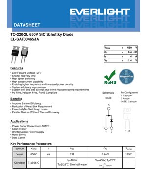
1. Product Overview
This document details the specifications for a high-performance Silicon Carbide (SiC) Schottky Barrier Diode. The device is engineered for power electronic applications requiring high efficiency, high-frequency operation, and superior thermal performance. Encapsulated in a standard TO-220-2L package, it offers a robust solution for demanding power conversion circuits.
The core advantage of this diode lies in its utilization of Silicon Carbide technology, which fundamentally provides a lower forward voltage drop and near-zero reverse recovery charge compared to traditional silicon PN-junction diodes. This translates directly into reduced conduction and switching losses, enabling higher system efficiency and power density.
2. In-Depth Technical Parameter Analysis
2.1 Electrical Characteristics
The key electrical parameters define the operational boundaries and performance of the device.
- Repetitive Peak Reverse Voltage (VRRM): 650V. This is the maximum instantaneous reverse voltage the diode can withstand repeatedly.
- Continuous Forward Current (IF): 4A. The maximum DC current the device can conduct continuously, limited by its thermal characteristics.
- Forward Voltage (VF): Typically 1.4V at IF=4A and Tj=25°C, with a maximum of 1.75V. This low VF is a hallmark of SiC Schottky technology, minimizing conduction losses.
- Reverse Current (IR): Typically 1µA at VR=520V and Tj=25°C. This low leakage current contributes to high efficiency in blocking state.
- Total Capacitive Charge (QC): 6.4nC (Typical) at VR=400V. This is a critical parameter for switching loss calculation, representing the charge that must be supplied/discharged during each switching cycle. The low value enables high-speed switching.
2.2 Maximum Ratings and Thermal Characteristics
Absolute maximum ratings define the stress limits beyond which permanent damage may occur.
- Surge Non-Repetitive Forward Current (IFSM): 19A for a 10ms half-sine wave pulse at Tc=25°C. This rating indicates the device's ability to handle short-circuit or inrush current events.
- Junction Temperature (TJ): Maximum 175°C. The upper limit for reliable operation.
- Total Power Dissipation (PD): 33W at Tc=25°C. This is the maximum power the package can dissipate under ideal cooling conditions at that case temperature.
- Thermal Resistance, Junction-to-Case (RθJC): 4.5°C/W (Typical). This low thermal resistance is crucial for effective heat transfer from the silicon die to the heatsink via the package case, enabling higher power handling.
3. Performance Curve Analysis
The datasheet provides several characteristic curves essential for design and simulation.
- VF-IF Characteristics: This graph shows the relationship between forward voltage and forward current at different junction temperatures. It is used to calculate conduction losses (Pcond = VF * IF).
- VR-IR Characteristics: Illustrates the reverse leakage current as a function of reverse voltage and temperature, important for assessing off-state losses.
- VR-Ct Characteristics: Shows how the diode's junction capacitance varies with applied reverse voltage. This non-linear capacitance impacts the switching speed and ringing.
- Maximum Ip – TC Characteristics: Depicts the derating of permissible forward current as a function of case temperature.
- Power Dissipation Derating Curve: Shows how the maximum allowable power dissipation decreases as the case temperature increases.
- IFSM – PW Characteristics: Provides the surge current capability for various pulse widths, essential for fuse selection and overload protection design.
- EC-VR Characteristics: Plots the stored capacitive energy (EC) against reverse voltage, derived from the capacitance curve, used for switching loss analysis.
- Transient Thermal Impedance Curve: Critical for evaluating thermal performance during short power pulses, where the thermal mass of the package becomes significant.
4. Mechanical and Package Information
4.1 Package Outline and Dimensions
The device uses the industry-standard TO-220-2L (2-Lead) through-hole package. Key dimensions include:
- Overall Length (D): 15.6 mm (Typical)
- Overall Width (E): 9.99 mm (Typical)
- Overall Height (A): 4.5 mm (Typical)
- Lead Pitch (e1): 5.08 mm (Basic)
- Mounting Hole Distance (E3): 8.70 mm (Reference)
- Mounting Hole Diameter: 1.70 mm (Reference)
The package is designed for easy mounting to a heatsink using an M3 or 6-32 screw, with a specified maximum mounting torque of 8.8 N·m.
4.2 Pin Configuration and Polarity Identification
The pinout is straightforward:
- Pin 1: Cathode (K)
- Pin 2: Anode (A)
- Case (Tab): Electrically connected to the Cathode (K). This connection is vital for both electrical circuit design and thermal management, as the tab is typically used for heatsinking.
A recommended surface-mount pad layout for the leads is also provided for PCB design reference.
5. Soldering and Assembly Guidelines
While specific reflow profiles are not detailed in this excerpt, general considerations for TO-220 packages apply:
- Handling: Observe standard ESD (Electrostatic Discharge) precautions as with all semiconductor devices.
- Mounting: Apply thermal interface material (grease or pad) between the package tab and the heatsink to minimize thermal resistance. Adhere to the specified 8.8 N·m maximum torque to avoid damaging the package or PCB.
- Soldering: For through-hole mounting, standard wave or hand soldering techniques can be used. The leads are suitable for clinching. The recommended pad layout should be followed for optimal solder joint formation and mechanical strength.
- Storage: Store in a dry, anti-static environment within the specified storage temperature range of -55°C to +175°C.
6. Application Suggestions
6.1 Typical Application Circuits
The datasheet explicitly lists several key applications where the benefits of SiC Schottky diodes are most pronounced:
- Power Factor Correction (PFC) in Switch-Mode Power Supplies (SMPS): The high switching speed and low Qc significantly reduce switching losses in the boost diode of PFC stages, improving overall efficiency, especially at high line frequencies.
- Solar Inverters: Used in the output rectification or freewheeling paths to minimize losses, increasing the energy harvest from photovoltaic panels.
- Uninterruptible Power Supplies (UPS): Enhances efficiency in the inverter/charger sections, leading to lower operating costs and reduced cooling requirements.
- Motor Drives: Serves as freewheeling diodes in inverter bridges, enabling higher switching frequencies for quieter motor operation and better control.
- Data Center Power Supplies: The drive for high efficiency (e.g., 80 Plus Titanium) in server PSUs makes the low-loss characteristics of this diode highly valuable.
6.2 Design Considerations
- Thermal Management: The low RθJC allows for effective cooling, but a properly sized heatsink is still essential to keep the junction temperature below 175°C under worst-case operating conditions. Use the power dissipation derating curve for design.
- Switching Behavior: While recovery losses are negligible, the capacitive switching behavior (defined by Qc) still requires consideration. The low Qc minimizes turn-on losses in the opposing switch in a bridge configuration.
- Parallel Operation: The positive temperature coefficient of the forward voltage (VF increases with temperature) aids in current sharing when multiple diodes are paralleled, helping to prevent thermal runaway.
- Snubber Circuits: Due to the very fast switching, attention should be paid to parasitic inductance in the circuit layout to minimize voltage overshoot and ringing. An RC snubber may be necessary depending on the layout.
7. Technical Comparison and Advantages
Compared to standard silicon fast recovery diodes (FRDs) or even ultrafast recovery diodes (UFRDs), this SiC Schottky diode offers distinct advantages:
- Essentially Zero Reverse Recovery Charge (Qrr): Unlike PN-junction diodes, Schottky diodes are majority carrier devices. They do not have a stored minority charge that must be recovered when switched from forward to reverse bias. This eliminates reverse recovery losses and associated noise.
- Lower Forward Voltage Drop: At typical operating currents, the VF of this SiC diode is competitive with or lower than high-voltage silicon Schottky diodes, which are generally limited to below 200V.
- High-Temperature Operation: Silicon Carbide material properties allow for reliable operation at higher junction temperatures (175°C max) compared to many silicon alternatives.
- Frequency Capability: The combination of low Qc and no Qrr enables operation at much higher switching frequencies, allowing for smaller magnetic components (inductors, transformers) and capacitors in the system.
8. Frequently Asked Questions (Based on Technical Parameters)
8.1 What is the main benefit of the low Qc (6.4nC) specification?
The low Total Capacitive Charge (Qc) directly translates to lower switching losses. During each switching cycle, the energy required to charge and discharge the diode's junction capacitance (E = 1/2 * C * V^2, or equivalently related to Qc) is lost. A lower Qc means less energy is wasted per cycle, enabling higher frequency operation with better efficiency.
8.2 The case is connected to the cathode. How does this affect my design?
This connection is crucial for two reasons: Electrically: The heatsink will be at cathode potential. You must ensure the heatsink is properly isolated from other components or chassis ground if the cathode is not at ground potential in your circuit. Insulating washers and bushings are typically required. Thermally: It provides an excellent low-impedance thermal path from the silicon die (junction) to the external heatsink via the metal tab, which is essential for dissipating heat.
8.3 Can I use this diode to replace a silicon diode with the same voltage/current rating?
Often, yes, but a direct replacement may not yield optimal results. The SiC diode will likely run cooler due to lower losses. However, you must re-evaluate: 1) Snubbing/Ringing: The faster switching may excite parasitic inductances more, potentially requiring layout changes or a snubber. 2) Gate Drive: If replacing a freewheeling diode in a bridge, the opposing switch may experience higher turn-on current spikes due to the diode's capacitance (though no reverse recovery). The driver should be checked for capability. 3) Thermal Design: While losses are lower, verify the new loss calculations and ensure the heatsink is still adequate, though it may now be oversized.
9. Practical Design Case Study
Scenario: Designing a 500W, 100kHz boost Power Factor Correction (PFC) stage with an output of 400VDC.
Selection Rationale: The boost diode in a PFC circuit operates in continuous conduction mode (CCM) at high frequency. A standard 600V silicon ultrafast diode might have a Qrr of 50-100nC and a Vf of 1.7-2.0V. The switching losses (proportional to Qrr * Vout * fsw) and conduction losses (Vf * Iavg) would be significant.
Using this SiC Schottky Diode:
- Switching Losses: Reverse recovery loss is eliminated. The remaining capacitive switching loss is based on Qc=6.4nC, which is an order of magnitude lower than the silicon diode's Qrr.
- Conduction Losses: With a typical Vf of 1.4V vs. 1.8V, conduction loss is reduced by over 20%.
- Result: The total diode loss is drastically reduced. This allows for either: a) Higher system efficiency, meeting stricter standards like 80 Plus Titanium, or b) Operation at an even higher switching frequency (e.g., 150-200kHz), enabling the use of a smaller, lighter boost inductor. The reduced heat generation also simplifies thermal management, potentially allowing for a smaller heatsink.
10. Operating Principle Introduction
A Schottky barrier diode is formed by a metal-semiconductor junction, unlike a standard diode's P-N semiconductor junction. In this SiC Schottky diode, a metal contact is made to Silicon Carbide (specifically, N-type SiC).
The fundamental difference lies in charge transport. In a PN diode, forward conduction involves injecting minority carriers (holes into the N-side, electrons into the P-side) which are stored. When the voltage reverses, these stored carriers must be removed (recombined or swept out) before the diode can block voltage, causing the reverse recovery current and loss.
In a Schottky diode, conduction occurs via the flow of majority carriers (electrons in N-SiC) over the metal-semiconductor barrier. No minority carriers are injected and stored. Therefore, when the applied voltage reverses, the diode can stop conducting almost instantaneously as the electrons are simply pulled back. This results in the characteristic near-zero reverse recovery time and charge (Qrr). The Silicon Carbide substrate provides the material properties necessary to achieve a high breakdown voltage (650V) while maintaining a relatively low forward voltage drop and excellent thermal conductivity.
11. Technology Trends
Silicon Carbide (SiC) power devices represent a significant trend in power electronics, driven by the global demand for higher efficiency, power density, and reliability. Key trends include:
- Voltage Scaling: While 650V is a mainstream voltage for applications like PFC and solar, SiC Schottky diodes are now commonly available at 1200V and 1700V, competing directly with silicon IGBT freewheeling diodes and enabling new applications in electric vehicle traction inverters and industrial drives.
- Integration: There is a move towards co-packaging SiC Schottky diodes with Silicon or SiC MOSFETs in common power modules, creating optimized "half-bridge" or "full-bridge" building blocks that minimize parasitic inductance.
- Cost Reduction: As wafer manufacturing scales and defect densities decrease, the cost premium of SiC over silicon continues to shrink, accelerating adoption in cost-sensitive high-volume applications like consumer power supplies and automotive.
- Complementary Technology: The development of SiC MOSFETs and JFETs is synergistic. Using a SiC Schottky diode as the freewheeling or boost diode alongside a SiC switch creates an all-SiC power stage capable of operating at very high frequencies and temperatures with minimal losses.
The device described in this datasheet is a foundational component within this broader technological shift towards wide-bandgap semiconductors in power conversion.
LED Specification Terminology
Complete explanation of LED technical terms
Photoelectric Performance
| Term | Unit/Representation | Simple Explanation | Why Important |
|---|---|---|---|
| Luminous Efficacy | lm/W (lumens per watt) | Light output per watt of electricity, higher means more energy efficient. | Directly determines energy efficiency grade and electricity cost. |
| Luminous Flux | lm (lumens) | Total light emitted by source, commonly called "brightness". | Determines if the light is bright enough. |
| Viewing Angle | ° (degrees), e.g., 120° | Angle where light intensity drops to half, determines beam width. | Affects illumination range and uniformity. |
| CCT (Color Temperature) | K (Kelvin), e.g., 2700K/6500K | Warmth/coolness of light, lower values yellowish/warm, higher whitish/cool. | Determines lighting atmosphere and suitable scenarios. |
| CRI / Ra | Unitless, 0–100 | Ability to render object colors accurately, Ra≥80 is good. | Affects color authenticity, used in high-demand places like malls, museums. |
| SDCM | MacAdam ellipse steps, e.g., "5-step" | Color consistency metric, smaller steps mean more consistent color. | Ensures uniform color across same batch of LEDs. |
| Dominant Wavelength | nm (nanometers), e.g., 620nm (red) | Wavelength corresponding to color of colored LEDs. | Determines hue of red, yellow, green monochrome LEDs. |
| Spectral Distribution | Wavelength vs intensity curve | Shows intensity distribution across wavelengths. | Affects color rendering and quality. |
Electrical Parameters
| Term | Symbol | Simple Explanation | Design Considerations |
|---|---|---|---|
| Forward Voltage | Vf | Minimum voltage to turn on LED, like "starting threshold". | Driver voltage must be ≥Vf, voltages add up for series LEDs. |
| Forward Current | If | Current value for normal LED operation. | Usually constant current drive, current determines brightness & lifespan. |
| Max Pulse Current | Ifp | Peak current tolerable for short periods, used for dimming or flashing. | Pulse width & duty cycle must be strictly controlled to avoid damage. |
| Reverse Voltage | Vr | Max reverse voltage LED can withstand, beyond may cause breakdown. | Circuit must prevent reverse connection or voltage spikes. |
| Thermal Resistance | Rth (°C/W) | Resistance to heat transfer from chip to solder, lower is better. | High thermal resistance requires stronger heat dissipation. |
| ESD Immunity | V (HBM), e.g., 1000V | Ability to withstand electrostatic discharge, higher means less vulnerable. | Anti-static measures needed in production, especially for sensitive LEDs. |
Thermal Management & Reliability
| Term | Key Metric | Simple Explanation | Impact |
|---|---|---|---|
| Junction Temperature | Tj (°C) | Actual operating temperature inside LED chip. | Every 10°C reduction may double lifespan; too high causes light decay, color shift. |
| Lumen Depreciation | L70 / L80 (hours) | Time for brightness to drop to 70% or 80% of initial. | Directly defines LED "service life". |
| Lumen Maintenance | % (e.g., 70%) | Percentage of brightness retained after time. | Indicates brightness retention over long-term use. |
| Color Shift | Δu′v′ or MacAdam ellipse | Degree of color change during use. | Affects color consistency in lighting scenes. |
| Thermal Aging | Material degradation | Deterioration due to long-term high temperature. | May cause brightness drop, color change, or open-circuit failure. |
Packaging & Materials
| Term | Common Types | Simple Explanation | Features & Applications |
|---|---|---|---|
| Package Type | EMC, PPA, Ceramic | Housing material protecting chip, providing optical/thermal interface. | EMC: good heat resistance, low cost; Ceramic: better heat dissipation, longer life. |
| Chip Structure | Front, Flip Chip | Chip electrode arrangement. | Flip chip: better heat dissipation, higher efficacy, for high-power. |
| Phosphor Coating | YAG, Silicate, Nitride | Covers blue chip, converts some to yellow/red, mixes to white. | Different phosphors affect efficacy, CCT, and CRI. |
| Lens/Optics | Flat, Microlens, TIR | Optical structure on surface controlling light distribution. | Determines viewing angle and light distribution curve. |
Quality Control & Binning
| Term | Binning Content | Simple Explanation | Purpose |
|---|---|---|---|
| Luminous Flux Bin | Code e.g., 2G, 2H | Grouped by brightness, each group has min/max lumen values. | Ensures uniform brightness in same batch. |
| Voltage Bin | Code e.g., 6W, 6X | Grouped by forward voltage range. | Facilitates driver matching, improves system efficiency. |
| Color Bin | 5-step MacAdam ellipse | Grouped by color coordinates, ensuring tight range. | Guarantees color consistency, avoids uneven color within fixture. |
| CCT Bin | 2700K, 3000K etc. | Grouped by CCT, each has corresponding coordinate range. | Meets different scene CCT requirements. |
Testing & Certification
| Term | Standard/Test | Simple Explanation | Significance |
|---|---|---|---|
| LM-80 | Lumen maintenance test | Long-term lighting at constant temperature, recording brightness decay. | Used to estimate LED life (with TM-21). |
| TM-21 | Life estimation standard | Estimates life under actual conditions based on LM-80 data. | Provides scientific life prediction. |
| IESNA | Illuminating Engineering Society | Covers optical, electrical, thermal test methods. | Industry-recognized test basis. |
| RoHS / REACH | Environmental certification | Ensures no harmful substances (lead, mercury). | Market access requirement internationally. |
| ENERGY STAR / DLC | Energy efficiency certification | Energy efficiency and performance certification for lighting. | Used in government procurement, subsidy programs, enhances competitiveness. |