Table of Contents
- 1. Product Overview
- 2. In-Depth Technical Parameter Analysis
- 2.1 Electrical Characteristics
- 2.2 Thermal Characteristics
- 3. Performance Curve Analysis
- 3.1 VF-IF Characteristics
- 3.2 VR-IR Characteristics
- 3.3 VR-Ct Characteristics
- 3.4 Maximum Forward Current vs. Case Temperature
- 3.5 Transient Thermal Impedance
- 4. Mechanical and Package Information
- 4.1 Package Outline and Dimensions
- 4.2 Pin Configuration and Polarity
- 5. Application Guidelines
- 5.1 Typical Application Scenarios
- 5.2 Design Considerations
- 6. Technical Comparison and Advantages
- 7. Frequently Asked Questions (FAQs)
- 8. Operational Principles
- 9. Industry Trends
1. Product Overview
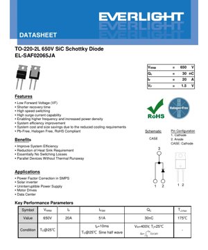
The EL-SAF02065JA is a high-performance Silicon Carbide (SiC) Schottky Barrier Diode (SBD) designed for demanding power electronics applications. Encapsulated in a standard TO-220-2L package, this device leverages the superior material properties of SiC to deliver significant advantages over traditional silicon-based diodes, particularly in high-frequency and high-efficiency power conversion systems.
Its core function is to provide unidirectional current flow with minimal switching losses and reverse recovery charge. The primary market for this component includes modern switch-mode power supplies (SMPS), renewable energy inverters, motor drives, and uninterruptible power supplies (UPS) where system efficiency, power density, and thermal management are critical design parameters.
2. In-Depth Technical Parameter Analysis
2.1 Electrical Characteristics
The electrical parameters define the operational boundaries and performance of the diode under specific conditions.
- Repetitive Peak Reverse Voltage (VRRM): 650V. This is the maximum instantaneous reverse voltage the diode can withstand repeatedly. It defines the voltage rating for the device in applications like power factor correction (PFC) circuits.
- Continuous Forward Current (IF): 20A. This is the maximum average forward current the diode can conduct continuously, limited by the junction-to-case thermal resistance and maximum junction temperature.
- Forward Voltage (VF): Typically 1.5V at IF=20A and Tj=25°C, with a maximum of 1.85V. This parameter directly impacts conduction losses. The datasheet also specifies VF at the maximum junction temperature (Tj=175°C), which is crucial for thermal design, showing a typical value of 1.9V.
- Reverse Current (IR): A key indicator of leakage. At VR=520V, IR is typically 4µA at 25°C and increases to 40µA at 175°C. This low leakage contributes to high efficiency, especially in standby modes.
- Total Capacitive Charge (QC): A critical parameter for switching loss calculation. At VR=400V and Tj=25°C, QC is typically 30nC. This low value is a hallmark of SiC Schottky diodes and is responsible for their "essentially no switching losses" characteristic compared to silicon PN junction diodes with high reverse recovery charge (Qrr).
- Surge Non-Repetitive Forward Current (IFSM): 51A for a 10ms half-sine wave pulse at Tc=25°C. This rating indicates the diode's ability to handle short-circuit or inrush current events.
2.2 Thermal Characteristics
Effective thermal management is essential for reliable operation and achieving rated performance.
- Maximum Junction Temperature (TJ): 175°C. This is the absolute maximum temperature the semiconductor junction can reach.
- Thermal Resistance, Junction-to-Case (RθJC): 2.0 °C/W (typical). This low thermal resistance is vital for efficient heat transfer from the silicon carbide die to the package case and, subsequently, to a heatsink. The power dissipation (PD) is listed as 75W at Tc=25°C, but this is primarily limited by the maximum TJ and RθJC in real applications.
- Mounting Torque (Md): Specified as 8.8 Nm for an M3 or 6-32 screw. Proper torque ensures optimal thermal contact between the package tab and the heatsink.
3. Performance Curve Analysis
The datasheet provides several characteristic curves essential for circuit design and simulation.
3.1 VF-IF Characteristics
This graph plots forward voltage drop against forward current, typically at multiple junction temperatures (e.g., 25°C, 125°C, 175°C). It shows the positive temperature coefficient of VF, which aids in current sharing when multiple diodes are connected in parallel, preventing thermal runaway—a significant benefit highlighted in the features.
3.2 VR-IR Characteristics
This curve illustrates the reverse leakage current as a function of the applied reverse voltage, again at various temperatures. It helps designers understand leakage power loss under different operating conditions.
3.3 VR-Ct Characteristics
This graph shows the junction capacitance (Ct) versus reverse voltage (VR). Capacitance decreases with increasing reverse bias (e.g., from ~513 pF at 1V to ~46 pF at 400V). This variable capacitance affects high-frequency switching behavior and resonant circuit designs.
3.4 Maximum Forward Current vs. Case Temperature
This derating curve shows how the maximum allowable continuous forward current (IF) decreases as the case temperature (Tc) increases. It is fundamental for selecting an appropriate heatsink to ensure the diode operates within its safe operating area (SOA).
3.5 Transient Thermal Impedance
The curve of transient thermal resistance (ZθJC) versus pulse width is critical for evaluating thermal performance under pulsed current conditions, which are common in switching applications. It allows calculation of peak junction temperature during switching events.
4. Mechanical and Package Information
4.1 Package Outline and Dimensions
The device uses the industry-standard TO-220-2L (two-lead) package. Key dimensions from the datasheet include:
- Overall Length (D): 15.6 mm (typ)
- Overall Width (E): 9.99 mm (typ)
- Overall Height (A): 4.5 mm (typ)
- Lead Pitch (e1): 5.08 mm (BSC, Basic Spacing between Centers)
- Mounting Hole Dimensions and recommended pad layout for surface mounting of the leadform are also provided, ensuring proper PCB design for thermal and electrical performance.
4.2 Pin Configuration and Polarity
The pinout is clearly defined:
- Pin 1: Cathode (K)
- Pin 2: Anode (A)
- Case (Tab): Electrically connected to the Cathode (K). This is crucial for proper mounting, as the tab must be isolated from the heatsink if the heatsink is not at cathode potential.
5. Application Guidelines
5.1 Typical Application Scenarios
- Power Factor Correction (PFC) in SMPS: The diode's high-speed switching and low Qc make it ideal for boost PFC stages, enabling higher switching frequencies, smaller magnetic components, and improved efficiency.
- Solar Inverters: Used in the boost stage or as freewheeling diodes, contributing to higher overall inverter efficiency and reliability.
- Uninterruptible Power Supplies (UPS): Improves efficiency in the inverter and converter sections, reducing energy loss and cooling requirements.
- Motor Drives: Serves as a freewheeling or clamping diode in inverter bridges, allowing for faster switching of IGBTs or MOSFETs and reducing voltage spikes.
- Data Center Power Supplies: The drive for high efficiency (e.g., 80 Plus Titanium) makes SiC diodes attractive for both PFC and DC-DC conversion stages.
5.2 Design Considerations
- Heatsinking: Due to the cathode-connected tab, electrical isolation (using a thermally conductive but electrically insulating pad) is mandatory if the heatsink is not at the same potential as the cathode.
- PCB Layout: Minimize parasitic inductance in the high-current loop (especially the loop formed by the switch, diode, and capacitor) to reduce voltage overshoot during switching transitions.
- Gate Drive Considerations: While the diode itself has no gate, its fast switching can induce high dV/dt and dI/dt in the circuit, which may affect the driving of associated MOSFETs or IGBTs. Proper snubber circuits or RC networks might be necessary in some designs.
- Parallel Operation: The positive temperature coefficient of VF facilitates current sharing in parallel configurations. However, layout symmetry and matched heatsinking are still recommended for optimal performance.
6. Technical Comparison and Advantages
Compared to standard silicon ultra-fast recovery diodes or even silicon Schottky diodes (which are limited to lower voltages, typically <200V), the EL-SAF02065JA offers distinct advantages:
- Near-Zero Reverse Recovery: The fundamental Schottky barrier mechanism in SiC eliminates the minority carrier storage time present in PN junction diodes, resulting in negligible reverse recovery charge (Qc vs. Qrr). This drastically reduces switching losses.
- High-Temperature Operation: SiC's wide bandgap allows a maximum junction temperature of 175°C, higher than most silicon devices, improving reliability under high ambient temperatures.
- High Voltage Rating: SiC material enables high breakdown voltages (650V here) while maintaining good on-state characteristics, a combination difficult to achieve with silicon Schottky diodes.
- System-Level Benefits: As listed in the features, these translate to higher frequency operation (smaller passives), increased power density, improved system efficiency, and potential savings on cooling system size and cost.
7. Frequently Asked Questions (FAQs)
Q: What is the main difference between Qc and Qrr?
A: Qc (Capacitive Charge) is the charge associated with charging and discharging the junction capacitance of a Schottky diode. Qrr (Reverse Recovery Charge) is the charge associated with removing stored minority carriers in a PN junction diode during turn-off. Qc is typically much smaller and results in lower switching loss.
Q: Why is the case connected to the cathode?
A: This is a common design in many power diodes and transistors. It simplifies internal package construction and provides a low-inductance, high-current path for the cathode connection via the mounting tab.
Q: Can this diode be used at its full 20A rating without a heatsink?
A: Almost certainly not. With an RθJC of 2.0°C/W and a VF of ~1.5V, power dissipation at 20A would be approximately 30W (P=Vf*If). This would cause a 60°C temperature rise from case to junction (ΔT = P * RθJC). Without a heatsink, the case temperature would quickly rise towards the maximum, exceeding Tj,max. Proper thermal design is essential.
Q: Is a snubber circuit required for this diode?
A> Due to its fast switching and low capacitance, ringing caused by circuit parasitics (inductance and capacitance) can be more pronounced. While the diode itself does not require a snubber, the overall circuit might benefit from an RC snubber across the diode or the main switch to dampen oscillations and reduce EMI.
8. Operational Principles
A Schottky diode is a majority carrier device formed by a metal-semiconductor junction. When a positive voltage is applied to the semiconductor (anode) relative to the metal (cathode), electrons flow easily from the semiconductor into the metal, allowing forward conduction with a relatively low voltage drop (typically 0.3-0.5V for silicon, 1.2-1.8V for SiC). The higher VF in SiC is due to its wider bandgap. Under reverse bias, the built-in potential of the junction prevents current flow, with only a small leakage current due to thermionic emission and quantum tunneling. The absence of minority carrier injection and storage is what eliminates the reverse recovery phenomenon seen in PN junction diodes.
9. Industry Trends
Silicon Carbide (SiC) power devices are a key enabling technology for the ongoing electrification and efficiency improvement across multiple industries. The market for SiC diodes and transistors is growing rapidly, driven by demands in electric vehicles (EVs), EV charging infrastructure, renewable energy, and high-efficiency industrial power supplies. Trends include increasing voltage and current ratings, improved reliability and yield leading to lower costs, and the integration of SiC diodes with SiC MOSFETs in power modules. The device described in this datasheet represents a mature and widely adopted component within this broader technological shift towards wide-bandgap semiconductors.
LED Specification Terminology
Complete explanation of LED technical terms
Photoelectric Performance
| Term | Unit/Representation | Simple Explanation | Why Important |
|---|---|---|---|
| Luminous Efficacy | lm/W (lumens per watt) | Light output per watt of electricity, higher means more energy efficient. | Directly determines energy efficiency grade and electricity cost. |
| Luminous Flux | lm (lumens) | Total light emitted by source, commonly called "brightness". | Determines if the light is bright enough. |
| Viewing Angle | ° (degrees), e.g., 120° | Angle where light intensity drops to half, determines beam width. | Affects illumination range and uniformity. |
| CCT (Color Temperature) | K (Kelvin), e.g., 2700K/6500K | Warmth/coolness of light, lower values yellowish/warm, higher whitish/cool. | Determines lighting atmosphere and suitable scenarios. |
| CRI / Ra | Unitless, 0–100 | Ability to render object colors accurately, Ra≥80 is good. | Affects color authenticity, used in high-demand places like malls, museums. |
| SDCM | MacAdam ellipse steps, e.g., "5-step" | Color consistency metric, smaller steps mean more consistent color. | Ensures uniform color across same batch of LEDs. |
| Dominant Wavelength | nm (nanometers), e.g., 620nm (red) | Wavelength corresponding to color of colored LEDs. | Determines hue of red, yellow, green monochrome LEDs. |
| Spectral Distribution | Wavelength vs intensity curve | Shows intensity distribution across wavelengths. | Affects color rendering and quality. |
Electrical Parameters
| Term | Symbol | Simple Explanation | Design Considerations |
|---|---|---|---|
| Forward Voltage | Vf | Minimum voltage to turn on LED, like "starting threshold". | Driver voltage must be ≥Vf, voltages add up for series LEDs. |
| Forward Current | If | Current value for normal LED operation. | Usually constant current drive, current determines brightness & lifespan. |
| Max Pulse Current | Ifp | Peak current tolerable for short periods, used for dimming or flashing. | Pulse width & duty cycle must be strictly controlled to avoid damage. |
| Reverse Voltage | Vr | Max reverse voltage LED can withstand, beyond may cause breakdown. | Circuit must prevent reverse connection or voltage spikes. |
| Thermal Resistance | Rth (°C/W) | Resistance to heat transfer from chip to solder, lower is better. | High thermal resistance requires stronger heat dissipation. |
| ESD Immunity | V (HBM), e.g., 1000V | Ability to withstand electrostatic discharge, higher means less vulnerable. | Anti-static measures needed in production, especially for sensitive LEDs. |
Thermal Management & Reliability
| Term | Key Metric | Simple Explanation | Impact |
|---|---|---|---|
| Junction Temperature | Tj (°C) | Actual operating temperature inside LED chip. | Every 10°C reduction may double lifespan; too high causes light decay, color shift. |
| Lumen Depreciation | L70 / L80 (hours) | Time for brightness to drop to 70% or 80% of initial. | Directly defines LED "service life". |
| Lumen Maintenance | % (e.g., 70%) | Percentage of brightness retained after time. | Indicates brightness retention over long-term use. |
| Color Shift | Δu′v′ or MacAdam ellipse | Degree of color change during use. | Affects color consistency in lighting scenes. |
| Thermal Aging | Material degradation | Deterioration due to long-term high temperature. | May cause brightness drop, color change, or open-circuit failure. |
Packaging & Materials
| Term | Common Types | Simple Explanation | Features & Applications |
|---|---|---|---|
| Package Type | EMC, PPA, Ceramic | Housing material protecting chip, providing optical/thermal interface. | EMC: good heat resistance, low cost; Ceramic: better heat dissipation, longer life. |
| Chip Structure | Front, Flip Chip | Chip electrode arrangement. | Flip chip: better heat dissipation, higher efficacy, for high-power. |
| Phosphor Coating | YAG, Silicate, Nitride | Covers blue chip, converts some to yellow/red, mixes to white. | Different phosphors affect efficacy, CCT, and CRI. |
| Lens/Optics | Flat, Microlens, TIR | Optical structure on surface controlling light distribution. | Determines viewing angle and light distribution curve. |
Quality Control & Binning
| Term | Binning Content | Simple Explanation | Purpose |
|---|---|---|---|
| Luminous Flux Bin | Code e.g., 2G, 2H | Grouped by brightness, each group has min/max lumen values. | Ensures uniform brightness in same batch. |
| Voltage Bin | Code e.g., 6W, 6X | Grouped by forward voltage range. | Facilitates driver matching, improves system efficiency. |
| Color Bin | 5-step MacAdam ellipse | Grouped by color coordinates, ensuring tight range. | Guarantees color consistency, avoids uneven color within fixture. |
| CCT Bin | 2700K, 3000K etc. | Grouped by CCT, each has corresponding coordinate range. | Meets different scene CCT requirements. |
Testing & Certification
| Term | Standard/Test | Simple Explanation | Significance |
|---|---|---|---|
| LM-80 | Lumen maintenance test | Long-term lighting at constant temperature, recording brightness decay. | Used to estimate LED life (with TM-21). |
| TM-21 | Life estimation standard | Estimates life under actual conditions based on LM-80 data. | Provides scientific life prediction. |
| IESNA | Illuminating Engineering Society | Covers optical, electrical, thermal test methods. | Industry-recognized test basis. |
| RoHS / REACH | Environmental certification | Ensures no harmful substances (lead, mercury). | Market access requirement internationally. |
| ENERGY STAR / DLC | Energy efficiency certification | Energy efficiency and performance certification for lighting. | Used in government procurement, subsidy programs, enhances competitiveness. |