Table of Contents
- 1. Product Overview
- 2. In-Depth Technical Parameter Analysis
- 2.1 Absolute Maximum Ratings
- 2.2 Electrical Characteristics
- 2.3 Thermal Characteristics
- 3. Performance Curve Analysis
- 3.1 VF-IF Characteristics
- 3.2 VR-IR Characteristics
- 3.3 VR-Ct Characteristics
- 3.4 Maximum Ip – TC Characteristics
- 3.5 IFSM – PW Characteristics
- 3.6 EC-VR Characteristics
- 3.7 Transient Thermal Resistance
- 4. Mechanical and Package Information
- 4.1 Package Outline and Dimensions
- 4.2 Pin Configuration and Polarity Identification
- 4.3 Recommended PCB Pad Layout
- 5. Soldering and Assembly Guidelines
- 6. Application Recommendations
- 6.1 Typical Application Circuits
- 6.2 Design Considerations
- 7. Technical Comparison and Advantages
- 8. Frequently Asked Questions (FAQ)
- 8.1 What does "essentially no switching losses" mean?
- 8.2 Why is the forward voltage positive temperature coefficient beneficial?
- 8.3 Can this diode be used in place of a standard silicon diode in an existing design?
- 8.4 How do I calculate the power loss for this diode?
- 9. Practical Design Case Study
- 10. Operating Principle
- 11. Technology Trends
- LED Specification Terminology
- Photoelectric Performance
- Electrical Parameters
- Thermal Management & Reliability
- Packaging & Materials
- Quality Control & Binning
- Testing & Certification
1. Product Overview
This document details the specifications for a high-performance Silicon Carbide (SiC) Schottky diode. The device is engineered for high-voltage, high-frequency power conversion applications where efficiency, thermal performance, and switching speed are critical. The TO-247-2L package offers a robust mechanical solution with excellent thermal characteristics, making it suitable for demanding industrial and renewable energy systems.
The core advantage of this SiC Schottky diode lies in its material properties. Unlike traditional silicon PN-junction diodes, the SiC Schottky barrier diode exhibits virtually no reverse recovery charge (Qrr), which is a primary source of switching losses and electromagnetic interference (EMI) in circuits. This characteristic is fundamental to its performance benefits.
2. In-Depth Technical Parameter Analysis
2.1 Absolute Maximum Ratings
The absolute maximum ratings define the stress limits beyond which permanent damage to the device may occur. These are not intended for normal operation.
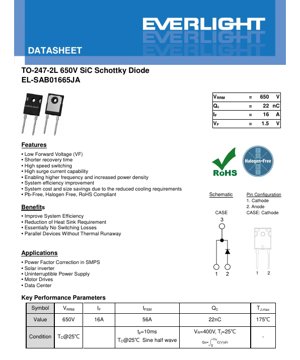
- Repetitive Peak Reverse Voltage (VRRM): 650V. This is the maximum instantaneous reverse voltage that can be applied repetitively.
- Surge Peak Reverse Voltage (VRSM): 650V. The maximum non-repetitive reverse voltage spike the device can withstand.
- Continuous Forward Current (IF): 16A. The maximum DC current the diode can conduct continuously, limited by the junction-to-case thermal resistance and maximum junction temperature.
- Surge Non-Repetitive Forward Current (IFSM): 56A at TC=25°C, tp=10ms, sine half-wave. This rating is crucial for assessing the diode's ability to handle short-circuit or inrush current events.
- Junction Temperature (TJ): 175°C maximum. Operating or storing the device above this temperature will degrade reliability.
2.2 Electrical Characteristics
These parameters define the device's performance under specified test conditions.
- Forward Voltage (VF): Typically 1.5V at IF=16A, TJ=25°C, with a maximum of 1.85V. This low VF is a key benefit of SiC technology, directly reducing conduction losses. At the maximum junction temperature of 175°C, VF increases to approximately 1.9V, showing a positive temperature coefficient.
- Reverse Current (IR): Typically 2µA at VR=520V, TJ=25°C, with a maximum of 60µA. The leakage current remains relatively low even at high temperature (30µA typical at 175°C), indicating good high-temperature blocking capability.
- Total Capacitive Charge (QC): 22nC typical at VR=400V, TJ=25°C. This parameter, along with the junction capacitance (C), is critical for calculating capacitive switching losses in high-frequency applications. The low QC value minimizes these losses.
- Capacitance Stored Energy (EC): 3.1µJ typical at VR=400V. This energy is dissipated during each switching cycle when charging and discharging the junction capacitance.
2.3 Thermal Characteristics
Thermal management is paramount for reliability and performance.
- Thermal Resistance, Junction-to-Case (RθJC): 1.3°C/W typical. This low value indicates excellent heat transfer from the semiconductor junction to the package case, allowing for efficient heat sinking. The case is electrically connected to the cathode.
- Total Power Dissipation (PD): 115W at TC=25°C. This is the maximum power the device can dissipate under ideal cooling conditions (case held at 25°C). In real applications, the allowable dissipation is lower based on the heatsink's thermal resistance and ambient temperature.
3. Performance Curve Analysis
The datasheet provides several characteristic curves essential for design.
3.1 VF-IF Characteristics
This graph shows the relationship between forward voltage and forward current at different junction temperatures. It demonstrates the diode's positive temperature coefficient for VF, which aids in current sharing when multiple devices are connected in parallel, helping to prevent thermal runaway.
3.2 VR-IR Characteristics
This curve plots reverse leakage current against reverse voltage at various temperatures. It is used to verify blocking performance and estimate off-state power losses.
3.3 VR-Ct Characteristics
This graph shows how the junction capacitance (Ct) decreases with increasing reverse voltage (VR). This non-linear characteristic is important for modeling switching behavior and resonant circuit design.
3.4 Maximum Ip – TC Characteristics
This curve defines the maximum allowable continuous forward current as a function of case temperature. It is derived from the power dissipation limit and thermal resistance, providing a practical guide for heatsink sizing.
3.5 IFSM – PW Characteristics
This graph illustrates the surge current capability for pulse widths (PW) other than the 10ms rating. It allows designers to assess the device's robustness against various fault conditions.
3.6 EC-VR Characteristics
This curve shows how the capacitive stored energy (EC) increases with reverse voltage (VR). This energy contributes to switching losses during turn-on.
3.7 Transient Thermal Resistance
The curve of transient thermal resistance versus pulse width (ZθJC) is critical for evaluating temperature rise during short power pulses. It shows that for very short pulses, the effective thermal resistance is lower than the steady-state value, as the heat has not yet spread through the entire package.
4. Mechanical and Package Information
4.1 Package Outline and Dimensions
The device is housed in a TO-247-2L package. The detailed mechanical drawing provides all critical dimensions including lead spacing, package height, and mounting hole location. The "2L" designation indicates a two-lead version. The case (tab) is electrically connected to the cathode terminal.
4.2 Pin Configuration and Polarity Identification
- Pin 1: Cathode (K).
- Pin 2: Anode (A).
- Case/Tab: Electrically connected to the Cathode (Pin 1). This connection must be considered for electrical isolation and heatsink mounting.
4.3 Recommended PCB Pad Layout
A suggested footprint for surface-mounting the leads is provided with dimensions. This layout ensures proper solder joint formation and mechanical stability. Adequate copper area around the mounting hole is recommended for thermal transfer to the PCB or an external heatsink.
5. Soldering and Assembly Guidelines
While specific reflow profiles are not provided in this datasheet, standard practices for power semiconductor devices in TO-247 packages apply.
- Mounting Torque: The recommended mounting torque for the screw (M3 or 6-32) is 8.8 Nm. Proper torque ensures good thermal contact between the package tab and the heatsink without damaging the package.
- Thermal Interface Material: A thin layer of thermal grease or a thermal pad is mandatory between the device tab and the heatsink to fill microscopic air gaps and minimize thermal resistance.
- Electrical Isolation: If the heatsink is not at cathode potential, a thermally conductive but electrically insulating spacer (e.g., mica washer, silicone pad) must be used between the device tab and the heatsink. The mounting hardware must also be insulated.
- Lead Forming: If leads need to be bent, it should be done carefully to avoid stress on the seal or internal connections. Bending should occur at a point more than 3mm from the package body.
- Storage Conditions: The device should be stored in a dry, anti-static environment within the temperature range of -55°C to +175°C.
6. Application Recommendations
6.1 Typical Application Circuits
- Power Factor Correction (PFC): Used as the boost diode in continuous conduction mode (CCM) or critical conduction mode (CrM) PFC stages. Its fast switching and low Qc enable higher switching frequencies, reducing the size of magnetic components.
- Solar Inverters: Employed in the boost stage of photovoltaic inverters and within the H-bridge or three-phase inverter output stage for freewheeling or clamping.
- Uninterruptible Power Supplies (UPS): Used in the rectifier/charger and inverter sections to improve efficiency and power density.
- Motor Drives: Serves as the freewheeling diode in inverter bridges driving AC motors, reducing switching losses and allowing for higher PWM frequencies, which can lower motor acoustic noise.
- Data Center Power Supplies: Applied in server power supplies (e.g., 80 Plus Titanium efficiency) and telecom rectifiers where peak efficiency is demanded.
6.2 Design Considerations
- Snubber Circuits: Due to the very fast switching and low recovery, snubber circuits may not be necessary for controlling voltage overshoot caused by reverse recovery. However, snubbers might still be needed to damp parasitic oscillations caused by circuit layout inductance and device capacitance.
- Gate Drive Considerations (for associated switches): When paired with a fast-switching SiC or GaN MOSFET, careful attention must be paid to gate drive loop inductance to minimize ringing and ensure clean switching transitions, maximizing the benefits of the diode's speed.
- Parallel Operation: The positive temperature coefficient of VF facilitates current sharing in parallel configurations. However, careful layout symmetry and matched heatsinking are still required for optimal performance.
- Heatsink Sizing: Use the maximum power dissipation formula: PD = (TJmax - TC) / RθJC. Determine the maximum allowable case temperature (TC) based on the worst-case ambient temperature and the selected heatsink's thermal resistance (RθSA).
7. Technical Comparison and Advantages
Compared to standard silicon fast recovery diodes (FRDs) or even silicon carbide MOSFET body diodes, this SiC Schottky diode offers distinct advantages:
- vs. Silicon FRDs: The most significant difference is the absence of reverse recovery charge (Qrr). A silicon FRD has substantial Qrr, causing high current spikes during turn-off, leading to significant switching losses, diode self-heating, and EMI. The SiC Schottky eliminates this, enabling higher frequency, higher efficiency, and simpler EMI filtering.
- vs. SiC MOSFET Body Diode: While the body diode of a SiC MOSFET is also made of SiC, it is a PN junction with poorer reverse recovery characteristics than a dedicated Schottky diode. Using a separate SiC Schottky as the freewheeling diode often results in lower total losses in hard-switching applications.
- System-Level Benefits: The reduction in switching and conduction losses allows for:
1. Higher switching frequencies, leading to smaller passive components (inductors, transformers, capacitors).
2. Reduced heatsink size and cost, or increased power output from the same thermal design.
3. Improved system efficiency, particularly at partial load, which is critical for energy-saving standards.
8. Frequently Asked Questions (FAQ)
8.1 What does "essentially no switching losses" mean?
It refers to the negligible reverse recovery loss. While there are still capacitive switching losses (related to QC and EC) and conduction losses (related to VF), the large reverse recovery loss present in silicon diodes is virtually eliminated. This makes the switching loss dominated by capacitance, which is much smaller.
8.2 Why is the forward voltage positive temperature coefficient beneficial?
In parallel operation, if one diode starts to carry more current and heats up, its VF increases slightly. This causes current to be redistributed to the cooler, lower-VF parallel devices, creating a natural balancing effect that prevents a single device from overheating—a condition known as thermal runaway.
8.3 Can this diode be used in place of a standard silicon diode in an existing design?
Not directly without analysis. While the pinout may be compatible, the faster switching can excite parasitic circuit elements, leading to voltage overshoot and ringing. The gate drive for the associated switch may need adjustment. Furthermore, the benefits are fully realized only when the circuit is optimized for higher frequency operation.
8.4 How do I calculate the power loss for this diode?
Total power loss (PD) is the sum of conduction loss and switching loss:
P_conduction = VF * IF * DutyCycle
P_switching = (EC * f_sw) (for capacitive loss)
Where f_sw is the switching frequency. Reverse recovery loss is negligible and can be omitted.
9. Practical Design Case Study
Scenario: Designing a 3kW, 80kHz boost PFC stage for a server power supply.
Challenge: Using a silicon FRD resulted in excessive switching losses and diode heating at 80kHz, limiting efficiency.
Solution: Replacing the silicon FRD with this SiC Schottky diode.
Outcome Analysis:
1. Loss Reduction: The Qrr-related loss (several watts) was eliminated. The remaining capacitive switching loss (EC * f_sw = ~0.25W) was manageable.
2. Thermal Improvement: Diode junction temperature dropped by over 30°C, allowing for a smaller heatsink or increased reliability.
3. System Impact: Overall PFC stage efficiency increased by ~0.7%, helping meet Titanium efficiency standards. The reduced diode heating also lowered the ambient temperature for nearby components.
10. Operating Principle
A Schottky diode is formed by a metal-semiconductor junction, unlike a standard diode's P-N semiconductor junction. In a Silicon Carbide Schottky diode, the metal is deposited on a wide-bandgap SiC semiconductor. The wide bandgap of SiC (approx. 3.26 eV for 4H-SiC vs. 1.12 eV for Si) allows for a much higher breakdown voltage with a thinner drift region, reducing on-resistance. The Schottky barrier results in a lower forward voltage drop than a PN junction for the same current density. Crucially, the switching action is governed by the majority carriers (electrons in an N-type SiC), so there is no minority carrier storage charge that needs to be removed during turn-off. This is the fundamental reason for the absence of reverse recovery.
11. Technology Trends
Silicon Carbide power devices are a key enabling technology for modern high-efficiency, high-power-density electronics. The trend is towards higher voltage ratings (1.2kV, 1.7kV, 3.3kV) for applications like electric vehicle traction inverters and industrial motor drives, and lower specific on-resistance (Rds(on)*Area) for reduced conduction losses. Concurrently, there is a drive to reduce the cost per amp of SiC devices through larger wafer diameters (transitioning from 150mm to 200mm) and improved manufacturing yields. Integration is another trend, with the development of modules containing multiple SiC MOSFETs and Schottky diodes in optimized topologies (e.g., half-bridge, boost). The device described in this datasheet represents a mature and widely adopted component within this evolving landscape.
LED Specification Terminology
Complete explanation of LED technical terms
Photoelectric Performance
| Term | Unit/Representation | Simple Explanation | Why Important |
|---|---|---|---|
| Luminous Efficacy | lm/W (lumens per watt) | Light output per watt of electricity, higher means more energy efficient. | Directly determines energy efficiency grade and electricity cost. |
| Luminous Flux | lm (lumens) | Total light emitted by source, commonly called "brightness". | Determines if the light is bright enough. |
| Viewing Angle | ° (degrees), e.g., 120° | Angle where light intensity drops to half, determines beam width. | Affects illumination range and uniformity. |
| CCT (Color Temperature) | K (Kelvin), e.g., 2700K/6500K | Warmth/coolness of light, lower values yellowish/warm, higher whitish/cool. | Determines lighting atmosphere and suitable scenarios. |
| CRI / Ra | Unitless, 0–100 | Ability to render object colors accurately, Ra≥80 is good. | Affects color authenticity, used in high-demand places like malls, museums. |
| SDCM | MacAdam ellipse steps, e.g., "5-step" | Color consistency metric, smaller steps mean more consistent color. | Ensures uniform color across same batch of LEDs. |
| Dominant Wavelength | nm (nanometers), e.g., 620nm (red) | Wavelength corresponding to color of colored LEDs. | Determines hue of red, yellow, green monochrome LEDs. |
| Spectral Distribution | Wavelength vs intensity curve | Shows intensity distribution across wavelengths. | Affects color rendering and quality. |
Electrical Parameters
| Term | Symbol | Simple Explanation | Design Considerations |
|---|---|---|---|
| Forward Voltage | Vf | Minimum voltage to turn on LED, like "starting threshold". | Driver voltage must be ≥Vf, voltages add up for series LEDs. |
| Forward Current | If | Current value for normal LED operation. | Usually constant current drive, current determines brightness & lifespan. |
| Max Pulse Current | Ifp | Peak current tolerable for short periods, used for dimming or flashing. | Pulse width & duty cycle must be strictly controlled to avoid damage. |
| Reverse Voltage | Vr | Max reverse voltage LED can withstand, beyond may cause breakdown. | Circuit must prevent reverse connection or voltage spikes. |
| Thermal Resistance | Rth (°C/W) | Resistance to heat transfer from chip to solder, lower is better. | High thermal resistance requires stronger heat dissipation. |
| ESD Immunity | V (HBM), e.g., 1000V | Ability to withstand electrostatic discharge, higher means less vulnerable. | Anti-static measures needed in production, especially for sensitive LEDs. |
Thermal Management & Reliability
| Term | Key Metric | Simple Explanation | Impact |
|---|---|---|---|
| Junction Temperature | Tj (°C) | Actual operating temperature inside LED chip. | Every 10°C reduction may double lifespan; too high causes light decay, color shift. |
| Lumen Depreciation | L70 / L80 (hours) | Time for brightness to drop to 70% or 80% of initial. | Directly defines LED "service life". |
| Lumen Maintenance | % (e.g., 70%) | Percentage of brightness retained after time. | Indicates brightness retention over long-term use. |
| Color Shift | Δu′v′ or MacAdam ellipse | Degree of color change during use. | Affects color consistency in lighting scenes. |
| Thermal Aging | Material degradation | Deterioration due to long-term high temperature. | May cause brightness drop, color change, or open-circuit failure. |
Packaging & Materials
| Term | Common Types | Simple Explanation | Features & Applications |
|---|---|---|---|
| Package Type | EMC, PPA, Ceramic | Housing material protecting chip, providing optical/thermal interface. | EMC: good heat resistance, low cost; Ceramic: better heat dissipation, longer life. |
| Chip Structure | Front, Flip Chip | Chip electrode arrangement. | Flip chip: better heat dissipation, higher efficacy, for high-power. |
| Phosphor Coating | YAG, Silicate, Nitride | Covers blue chip, converts some to yellow/red, mixes to white. | Different phosphors affect efficacy, CCT, and CRI. |
| Lens/Optics | Flat, Microlens, TIR | Optical structure on surface controlling light distribution. | Determines viewing angle and light distribution curve. |
Quality Control & Binning
| Term | Binning Content | Simple Explanation | Purpose |
|---|---|---|---|
| Luminous Flux Bin | Code e.g., 2G, 2H | Grouped by brightness, each group has min/max lumen values. | Ensures uniform brightness in same batch. |
| Voltage Bin | Code e.g., 6W, 6X | Grouped by forward voltage range. | Facilitates driver matching, improves system efficiency. |
| Color Bin | 5-step MacAdam ellipse | Grouped by color coordinates, ensuring tight range. | Guarantees color consistency, avoids uneven color within fixture. |
| CCT Bin | 2700K, 3000K etc. | Grouped by CCT, each has corresponding coordinate range. | Meets different scene CCT requirements. |
Testing & Certification
| Term | Standard/Test | Simple Explanation | Significance |
|---|---|---|---|
| LM-80 | Lumen maintenance test | Long-term lighting at constant temperature, recording brightness decay. | Used to estimate LED life (with TM-21). |
| TM-21 | Life estimation standard | Estimates life under actual conditions based on LM-80 data. | Provides scientific life prediction. |
| IESNA | Illuminating Engineering Society | Covers optical, electrical, thermal test methods. | Industry-recognized test basis. |
| RoHS / REACH | Environmental certification | Ensures no harmful substances (lead, mercury). | Market access requirement internationally. |
| ENERGY STAR / DLC | Energy efficiency certification | Energy efficiency and performance certification for lighting. | Used in government procurement, subsidy programs, enhances competitiveness. |