1. Product Overview
This document details the specifications for a high-performance Silicon Carbide (SiC) Schottky Barrier Diode (SBD) in a surface-mount TO-252-3L (DPAK) package. The device is engineered for high-voltage, high-frequency power conversion applications where efficiency, power density, and thermal management are critical. Utilizing SiC technology, this diode offers significant advantages over traditional silicon PN junction diodes, particularly in reducing switching losses and enabling higher operating frequencies.
The core positioning of this component is within advanced power supply and energy conversion systems. Its primary advantages stem from the inherent material properties of Silicon Carbide, which allow for a much lower reverse recovery charge and faster switching speeds compared to silicon counterparts. This directly translates to reduced switching losses in circuits, leading to higher overall system efficiency.
The target markets and applications are diverse, focusing on modern, efficient power electronics. Key sectors include industrial motor drives, renewable energy systems like solar inverters, server and data center power supplies, and uninterruptible power supplies (UPS). These applications benefit immensely from the diode's ability to operate at higher frequencies, which allows for the use of smaller passive components like inductors and capacitors, thereby increasing power density and potentially reducing system size and cost.
2. In-Depth Technical Parameter Analysis
2.1 Absolute Maximum Ratings
The absolute maximum ratings define the stress limits beyond which permanent damage to the device may occur. These are not intended for normal operation.
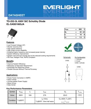
- Repetitive Peak Reverse Voltage (VRRM): 650V. This is the maximum reverse voltage that can be applied repetitively.
- Continuous Forward Current (IF): 16A. This is the maximum continuous forward current the diode can handle, limited by the maximum junction temperature and thermal resistance.
- Surge Non-Repetitive Forward Current (IFSM): 27A. This rating specifies the maximum allowable surge current for a short duration (10ms, half-sine wave), crucial for handling inrush or fault conditions.
- Junction Temperature (TJ): 175°C. The maximum allowable temperature of the semiconductor junction.
- Total Power Dissipation (PD): 70W. The maximum power the package can dissipate at a case temperature of 25°C.
2.2 Electrical Characteristics
These parameters define the device's performance under specified test conditions.
- Forward Voltage (VF): Typically 1.5V at 16A and 25°C junction temperature, with a maximum of 1.85V. This low VF is a key benefit of SiC Schottky technology, leading to lower conduction losses. Note that VF increases with temperature, reaching approximately 1.9V at 175°C.
- Reverse Current (IR): Typically 2µA at 520V and 25°C, with a maximum of 60µA. This low leakage current contributes to high efficiency in blocking states.
- Total Capacitive Charge (QC): 22 nC (typical) at 400V. This is a critical parameter for switching loss calculation. The low QC value indicates minimal stored charge that needs to be removed during turn-off, leading to essentially no reverse recovery current and very low switching losses.
- Total Capacitance (Ct): This is voltage-dependent. It measures 402 pF at 1V, 43 pF at 200V, and 32 pF at 400V (typical, at 1MHz). The decrease with increasing reverse voltage is characteristic of junction capacitance.
2.3 Thermal Characteristics
Thermal management is paramount for reliability and performance.
- Thermal Resistance, Junction-to-Case (RθJC): 2.9 °C/W (typical). This low value indicates efficient heat transfer from the semiconductor junction to the package case, which is essential for dissipating the generated heat into a heatsink or PCB.
3. Performance Curve Analysis
The datasheet provides several characteristic curves essential for design.
3.1 VF-IF Characteristics
This graph shows the relationship between forward voltage and forward current at different junction temperatures. It visually demonstrates the low forward voltage drop and its positive temperature coefficient. Designers use this to calculate conduction losses (Pcond = VF * IF) and understand how losses change with temperature.
3.2 VR-IR Characteristics
This curve plots reverse leakage current against reverse voltage at different temperatures. It confirms the low leakage current even at high voltages and elevated temperatures, which is vital for efficiency in blocking mode.
3.3 Maximum Forward Current vs. Case Temperature
This derating curve shows how the maximum allowable continuous forward current decreases as the case temperature (TC) increases. It is a crucial tool for thermal design, ensuring the diode is not operated beyond its safe operating area (SOA).
3.4 Power Dissipation vs. Case Temperature
Similar to the current derating, this curve shows the maximum allowable power dissipation as a function of case temperature.
3.5 Transient Thermal Impedance
This graph is critical for evaluating thermal performance during short power pulses. It shows the effective thermal resistance from junction to case for single pulses of varying width. This data is used to calculate the peak junction temperature rise during switching events, which is often more stressful than steady-state conditions.
4. Mechanical and Package Information
4.1 Package Dimensions (TO-252-3L)
The diode is housed in a TO-252-3L package, also known as DPAK. Key dimensions include:
- Package Length (E): 6.60 mm (typ)
- Package Width (D): 6.10 mm (typ)
- Package Height (H): 9.84 mm (typ)
- Lead Pitch (e1): 2.28 mm (basic)
- Lead Length (L): 1.52 mm (typ)
The detailed drawing provides all critical tolerances for PCB footprint design and assembly.
4.2 Pin Configuration and Polarity
The package has three connections: two leads and the case (tab).
- Pin 1: Cathode (K)
- Pin 2: Anode (A)
- Case (Tab): This is internally connected to the Cathode (K). This is a critical detail for PCB layout and heatsinking, as the tab must be electrically isolated from other circuits if they are not at cathode potential.
4.3 Recommended PCB Pad Layout
A suggested footprint for surface-mount assembly is provided. This layout is designed to ensure reliable solder joint formation, proper thermal relief, and effective heat dissipation into the PCB copper. Adhering to this recommendation is important for manufacturing yield and long-term reliability.
5. Application Guidelines and Design Considerations
5.1 Typical Application Circuits
This SiC Schottky diode is ideally suited for several key power conversion topologies:
- Power Factor Correction (PFC): Used in the boost converter stage of switched-mode power supplies (SMPS). Its high-speed switching reduces losses at high frequencies, improving PFC stage efficiency.
- Solar Inverter DC-AC Stage: Often used in the inverter's freewheeling or clamping circuits. The high voltage rating and low switching losses are beneficial for the high DC bus voltages and switching frequencies common in solar applications.
- Motor Drive Inverters: Serves as the freewheeling diode across Insulated-Gate Bipolar Transistors (IGBTs) or MOSFETs. Fast recovery minimizes dead-time requirements and reduces voltage spikes.
- Uninterruptible Power Supplies (UPS) and Data Center Power Supplies: Used in both PFC and DC-DC conversion stages to achieve high efficiency, which is critical for reducing energy consumption and cooling needs.
5.2 Key Design Considerations
- Thermal Management: Despite its low losses, proper heatsinking is essential. The low RθJC allows heat to be efficiently transferred to the PCB or an external heatsink. The mounting tab (cathode) must be soldered to a sufficiently large copper area on the PCB to act as a heatsink. For high-power applications, an external heatsink attached to the tab may be necessary.
- Paralleling Devices: SiC Schottky diodes have a positive temperature coefficient for forward voltage. This characteristic promotes current sharing between parallel devices, helping to prevent thermal runaway—a significant advantage over some other diode technologies.
- Switching Speed and Layout: The diode's ultra-fast switching capability means circuit layout is critical. Minimizing parasitic inductance in the power loop is necessary to avoid excessive voltage overshoot during turn-off. This involves using short, wide traces and proper placement of decoupling capacitors.
- Gate Drive Considerations (for associated switches): The lack of reverse recovery current simplifies the design of gate drive circuits for the accompanying switching transistors (e.g., MOSFETs, IGBTs), as there is no concern for shoot-through current caused by diode recovery.
6. Technical Comparison and Advantages
Compared to standard silicon fast recovery diodes (FRDs) or even silicon carbide junction barrier Schottky (JBS) diodes, this component offers distinct benefits:
- vs. Silicon PN Diodes: The most significant difference is the near-zero reverse recovery charge (Qrr), which is essentially replaced by the capacitive charge (Qc). This eliminates reverse recovery losses and associated EMI, allowing for much higher switching frequencies (tens to hundreds of kHz).
- vs. Silicon Schottky Diodes: Silicon Schottky diodes are limited to lower voltage ratings (typically below 200V). This SiC diode extends the benefits of the Schottky rectification principle (low VF, fast switching) to the 650V class, which is standard for many offline power applications.
- High-Temperature Operation: SiC material can operate at higher junction temperatures than silicon, enhancing reliability in harsh environments.
- System-Level Benefits: The enabling of higher switching frequencies allows for a reduction in the size of magnetic components (inductors, transformers) and capacitors, leading to more compact and lighter power supplies. The improved efficiency reduces heat generation, which can simplify or eliminate cooling systems, further reducing cost and size.
7. Frequently Asked Questions (FAQs)
7.1 What does \"essentially no switching losses\" mean?
Unlike silicon PN diodes that store minority carriers which must be removed during turn-off (causing a large reverse recovery current and significant loss), SiC Schottky diodes are majority carrier devices. Their turn-off behavior is dominated by the discharge of the junction capacitance (Qc). The energy lost is related to charging and discharging this capacitance (E = 1/2 * C * V^2), which is typically much lower than the reverse recovery losses of a comparable silicon diode.
7.2 Why is the forward voltage temperature coefficient positive?
In Schottky diodes, the forward voltage decreases slightly with temperature for a given current due to a decrease in the Schottky barrier height. However, the dominant effect in high-current SiC Schottky diodes is the increase in the resistance of the drift region with temperature. This increase in resistance causes the overall forward voltage to rise as temperature increases, providing the beneficial positive temperature coefficient for current sharing.
7.3 How do I calculate the junction temperature in my application?
The steady-state junction temperature can be estimated using: TJ = TC + (PD * RθJC). Where TC is the measured case temperature, PD is the power dissipated in the diode (conduction loss + switching loss), and RθJC is the thermal resistance. For dynamic conditions, the transient thermal impedance curve must be used with the power dissipation waveform.
7.4 Can I use this diode for 400V AC rectification?
For rectifying 400V AC line voltage, the peak reverse voltage can be as high as ~565V (400V * √2). A 650V-rated diode provides a safety margin for voltage spikes and transients on the line, making it a suitable and common choice for such applications, including three-phase 400VAC systems.
8. Practical Design Example
Scenario: Designing a 1.5kW boost Power Factor Correction (PFC) stage for a server power supply, targeting an input voltage range of 85-265VAC and an output of 400VDC. The switching frequency is set to 100 kHz to reduce magnetic size.
Diode Selection Rationale: A standard silicon ultrafast diode would have substantial reverse recovery losses at 100 kHz, severely impacting efficiency. This 650V SiC Schottky diode is chosen because its switching losses are negligible (based on Qc), and its conduction loss (based on VF) is low. The 16A continuous current rating is sufficient for the average and RMS currents in this application with appropriate derating.
Thermal Design: Calculations show a diode conduction loss of approximately 4W. Using the typical RθJC of 2.9°C/W, if the case temperature is maintained at 80°C, the junction temperature rise would be ~11.6°C, resulting in a TJ of ~91.6°C, which is well within the 175°C maximum. This allows the use of a PCB copper pad as the primary heatsink without requiring a bulky external heatsink, saving space and cost.
9. Technology Introduction and Trends
9.1 Silicon Carbide (SiC) Technology Principle
Silicon Carbide is a wide-bandgap semiconductor material. Its wider bandgap (approximately 3.26 eV for 4H-SiC vs. 1.12 eV for Si) gives it several superior physical properties: a much higher critical electric field (allowing for thinner, lower-resistance drift layers for a given voltage rating), higher thermal conductivity (improving heat dissipation), and the ability to operate at much higher temperatures. In Schottky diodes, SiC enables the combination of high breakdown voltage, low forward voltage drop, and extremely fast switching—a combination difficult to achieve with silicon.
9.2 Industry Trends
The adoption of SiC power devices, including Schottky diodes and MOSFETs, is accelerating. Key drivers are the global push for energy efficiency across all sectors (industrial, automotive, consumer) and the demand for higher power density. As manufacturing volumes increase and costs continue to decrease, SiC is moving from niche, high-performance applications into mainstream power supplies, electric vehicle onboard chargers, and solar energy systems. The trend is towards higher voltage ratings (e.g., 1200V, 1700V) for automotive and industrial drives, and the integration of SiC diodes with SiC MOSFETs in power modules for complete, high-performance switching cells.
LED Specification Terminology
Complete explanation of LED technical terms
Photoelectric Performance
| Term | Unit/Representation | Simple Explanation | Why Important |
|---|---|---|---|
| Luminous Efficacy | lm/W (lumens per watt) | Light output per watt of electricity, higher means more energy efficient. | Directly determines energy efficiency grade and electricity cost. |
| Luminous Flux | lm (lumens) | Total light emitted by source, commonly called "brightness". | Determines if the light is bright enough. |
| Viewing Angle | ° (degrees), e.g., 120° | Angle where light intensity drops to half, determines beam width. | Affects illumination range and uniformity. |
| CCT (Color Temperature) | K (Kelvin), e.g., 2700K/6500K | Warmth/coolness of light, lower values yellowish/warm, higher whitish/cool. | Determines lighting atmosphere and suitable scenarios. |
| CRI / Ra | Unitless, 0–100 | Ability to render object colors accurately, Ra≥80 is good. | Affects color authenticity, used in high-demand places like malls, museums. |
| SDCM | MacAdam ellipse steps, e.g., "5-step" | Color consistency metric, smaller steps mean more consistent color. | Ensures uniform color across same batch of LEDs. |
| Dominant Wavelength | nm (nanometers), e.g., 620nm (red) | Wavelength corresponding to color of colored LEDs. | Determines hue of red, yellow, green monochrome LEDs. |
| Spectral Distribution | Wavelength vs intensity curve | Shows intensity distribution across wavelengths. | Affects color rendering and quality. |
Electrical Parameters
| Term | Symbol | Simple Explanation | Design Considerations |
|---|---|---|---|
| Forward Voltage | Vf | Minimum voltage to turn on LED, like "starting threshold". | Driver voltage must be ≥Vf, voltages add up for series LEDs. |
| Forward Current | If | Current value for normal LED operation. | Usually constant current drive, current determines brightness & lifespan. |
| Max Pulse Current | Ifp | Peak current tolerable for short periods, used for dimming or flashing. | Pulse width & duty cycle must be strictly controlled to avoid damage. |
| Reverse Voltage | Vr | Max reverse voltage LED can withstand, beyond may cause breakdown. | Circuit must prevent reverse connection or voltage spikes. |
| Thermal Resistance | Rth (°C/W) | Resistance to heat transfer from chip to solder, lower is better. | High thermal resistance requires stronger heat dissipation. |
| ESD Immunity | V (HBM), e.g., 1000V | Ability to withstand electrostatic discharge, higher means less vulnerable. | Anti-static measures needed in production, especially for sensitive LEDs. |
Thermal Management & Reliability
| Term | Key Metric | Simple Explanation | Impact |
|---|---|---|---|
| Junction Temperature | Tj (°C) | Actual operating temperature inside LED chip. | Every 10°C reduction may double lifespan; too high causes light decay, color shift. |
| Lumen Depreciation | L70 / L80 (hours) | Time for brightness to drop to 70% or 80% of initial. | Directly defines LED "service life". |
| Lumen Maintenance | % (e.g., 70%) | Percentage of brightness retained after time. | Indicates brightness retention over long-term use. |
| Color Shift | Δu′v′ or MacAdam ellipse | Degree of color change during use. | Affects color consistency in lighting scenes. |
| Thermal Aging | Material degradation | Deterioration due to long-term high temperature. | May cause brightness drop, color change, or open-circuit failure. |
Packaging & Materials
| Term | Common Types | Simple Explanation | Features & Applications |
|---|---|---|---|
| Package Type | EMC, PPA, Ceramic | Housing material protecting chip, providing optical/thermal interface. | EMC: good heat resistance, low cost; Ceramic: better heat dissipation, longer life. |
| Chip Structure | Front, Flip Chip | Chip electrode arrangement. | Flip chip: better heat dissipation, higher efficacy, for high-power. |
| Phosphor Coating | YAG, Silicate, Nitride | Covers blue chip, converts some to yellow/red, mixes to white. | Different phosphors affect efficacy, CCT, and CRI. |
| Lens/Optics | Flat, Microlens, TIR | Optical structure on surface controlling light distribution. | Determines viewing angle and light distribution curve. |
Quality Control & Binning
| Term | Binning Content | Simple Explanation | Purpose |
|---|---|---|---|
| Luminous Flux Bin | Code e.g., 2G, 2H | Grouped by brightness, each group has min/max lumen values. | Ensures uniform brightness in same batch. |
| Voltage Bin | Code e.g., 6W, 6X | Grouped by forward voltage range. | Facilitates driver matching, improves system efficiency. |
| Color Bin | 5-step MacAdam ellipse | Grouped by color coordinates, ensuring tight range. | Guarantees color consistency, avoids uneven color within fixture. |
| CCT Bin | 2700K, 3000K etc. | Grouped by CCT, each has corresponding coordinate range. | Meets different scene CCT requirements. |
Testing & Certification
| Term | Standard/Test | Simple Explanation | Significance |
|---|---|---|---|
| LM-80 | Lumen maintenance test | Long-term lighting at constant temperature, recording brightness decay. | Used to estimate LED life (with TM-21). |
| TM-21 | Life estimation standard | Estimates life under actual conditions based on LM-80 data. | Provides scientific life prediction. |
| IESNA | Illuminating Engineering Society | Covers optical, electrical, thermal test methods. | Industry-recognized test basis. |
| RoHS / REACH | Environmental certification | Ensures no harmful substances (lead, mercury). | Market access requirement internationally. |
| ENERGY STAR / DLC | Energy efficiency certification | Energy efficiency and performance certification for lighting. | Used in government procurement, subsidy programs, enhances competitiveness. |