Table of Contents
- 1. Product Overview
- 2. In-Depth Technical Parameter Analysis
- 2.1 Electrical Characteristics
- 2.2 Maximum Ratings and Thermal Characteristics
- 3. Performance Curve Analysis
- 4. Mechanical and Package Information
- 4.1 Package Dimensions
- 4.2 Pin Configuration and Polarity
- 4.3 Recommended PCB Pad Layout
- 5. Soldering and Assembly Guidelines
- 6. Application Suggestions
- 6.1 Typical Application Circuits
- 6.2 Design Considerations
- 7. Technical Comparison and Advantages
- 8. Frequently Asked Questions (Based on Technical Parameters)
- 9. Practical Design Case Study
- 10. Operating Principle Introduction
- 11. Technology Trends
1. Product Overview
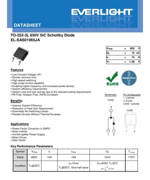
This document provides the complete technical specifications for a high-performance Silicon Carbide (SiC) Schottky Barrier Diode (SBD). The device is designed for high-voltage, high-frequency switching applications where efficiency and thermal management are critical. It is housed in a surface-mount TO-252-3L (DPAK) package, offering a robust thermal and electrical interface for power circuit designs.
The core advantage of this SiC Schottky diode lies in its material properties. Unlike traditional silicon PN-junction diodes, a Schottky diode has a metal-semiconductor junction, which inherently provides a lower forward voltage drop (VF) and, crucially, near-zero reverse recovery charge (Qc). This combination significantly reduces both conduction and switching losses, enabling higher system efficiency and power density.
The target markets for this component are advanced power conversion systems. Its primary benefits of high efficiency and high-speed switching make it ideal for modern, compact, and high-reliability power supplies.
2. In-Depth Technical Parameter Analysis
2.1 Electrical Characteristics
The electrical parameters define the operational boundaries and performance of the diode under various conditions.
- Repetitive Peak Reverse Voltage (VRRM): 650V. This is the maximum reverse voltage the diode can withstand repeatedly. It defines the voltage rating for applications like Power Factor Correction (PFC) stages operating from universal AC mains (85-265VAC).
- Continuous Forward Current (IF): 10A. This is the maximum average forward current the device can conduct continuously, limited by its thermal characteristics. The datasheet specifies this at a case temperature (TC) of 25°C.
- Forward Voltage (VF): 1.48V (Typ.) at IF=10A, TJ=25°C. This low VF is a key benefit of the SiC Schottky technology, directly reducing conduction losses (Ploss = VF * IF). Note that VF has a positive temperature coefficient, increasing to approximately 1.9V at 175°C junction temperature.
- Reverse Current (IR): 2µA (Typ.) at VR=520V, TJ=25°C. This low leakage current contributes to high efficiency in blocking state.
- Total Capacitive Charge (Qc): 15nC (Typ.) at VR=400V. This is arguably the most critical parameter for switching performance. Qc represents the charge that must be supplied/displaced to change the voltage across the diode's junction capacitance. A low Qc translates to minimal switching losses and enables operation at very high frequencies.
- Capacitance Stored Energy (EC): 2.2µJ (Typ.) at VR=400V. This parameter, derived from the junction capacitance, indicates the energy stored in the diode's electric field when reverse-biased. It must be considered in resonant circuit designs.
2.2 Maximum Ratings and Thermal Characteristics
These parameters define the absolute limits for safe operation and the device's ability to manage heat.
- Surge Non-Repetitive Forward Current (IFSM): 16A for a 10ms half-sine wave. This rating indicates the diode's ability to withstand short-term overloads, such as inrush currents.
- Junction Temperature (TJ): Maximum 175°C. Operating the device above this temperature can cause permanent damage.
- Thermal Resistance, Junction-to-Case (RθJC): 3.2°C/W (Typ.). This low thermal resistance is crucial for effective heat transfer from the silicon die to the package case and, subsequently, to the heatsink or PCB. The total power dissipation (PD) is listed as 44W, but this is primarily limited by the maximum TJ and the system's ability to remove heat (RθCA).
3. Performance Curve Analysis
The datasheet includes several characteristic curves essential for design engineers.
- VF-IF Characteristics: This graph shows the relationship between forward voltage and forward current at different junction temperatures. It is used to calculate precise conduction losses under actual operating conditions, not just at the 25°C typical point.
- VR-IR Characteristics: Illustrates the reverse leakage current as a function of reverse voltage and temperature. This is critical for estimating standby losses and ensuring stable blocking performance at high temperatures.
- VR-Ct Characteristics: Shows how the total diode capacitance (Ct) decreases with increasing reverse voltage (VR). This non-linear capacitance impacts high-frequency switching behavior and resonant circuit design.
- Maximum IF vs. Case Temperature (TC): A derating curve that defines how the maximum allowable continuous forward current decreases as the case temperature rises. This is fundamental for thermal design.
- Power Dissipation vs. Case Temperature: Similar to the current derating, this curve shows how much power the device can dissipate based on its case temperature.
- IFSM vs. Pulse Width (PW): Provides the surge current capability for pulse durations other than the standard 10ms, allowing assessment of fault condition tolerance.
- EC-VR Characteristics: Graphs the stored capacitive energy versus reverse voltage, useful for loss calculations in soft-switching topologies.
- Transient Thermal Resistance (ZθJC) vs. Pulse Width: This curve is vital for evaluating thermal performance during short switching pulses. The effective thermal resistance for a single short pulse is lower than the steady-state RθJC.
4. Mechanical and Package Information
4.1 Package Dimensions
The device uses the industry-standard TO-252-3L (DPAK) surface-mount package. Key dimensions from the outline drawing include:
- Overall Length (H): 9.84 mm (Typ.)
- Overall Width (E): 6.60 mm (Typ.)
- Overall Height (A): 2.30 mm (Typ.)
- Lead Pitch (e1): 2.28 mm (Basic)
- Tab Dimensions (D1 x E1): 5.23 mm x 4.83 mm (Typ.)
The large metal tab serves as the primary thermal path (connected to the cathode) and must be properly soldered to a corresponding copper pad on the PCB for effective heat sinking.
4.2 Pin Configuration and Polarity
The pinout is clearly defined:
- Pin 1: Cathode (K)
- Pin 2: Anode (A)
- Case (Tab): Cathode (K)
Important: The case (the large metal tab) is electrically connected to the cathode. This must be considered during PCB layout to avoid short circuits. The tab must be isolated from other nets unless intentionally connected to the cathode node.
4.3 Recommended PCB Pad Layout
A suggested footprint for surface mounting is provided. This layout is optimized for solder joint reliability and thermal performance. It typically includes a large central pad for the tab with thermal vias to inner copper layers or a bottom-side heatsink, plus two smaller pads for the anode and cathode leads.
5. Soldering and Assembly Guidelines
While specific reflow profiles are not detailed in this excerpt, general guidelines for power SMD packages apply.
- Reflow Soldering: Standard lead-free (Pb-Free) reflow profiles are suitable. The large thermal mass of the tab may require slight profile adjustments (e.g., longer soak time or higher peak temperature) to ensure complete solder reflow under the tab.
- Thermal Vias: For optimal thermal performance, the PCB pad for the tab should incorporate multiple thermal vias filled with solder during reflow. These vias conduct heat to internal ground planes or a bottom-side copper pour.
- Mounting Torque: If an additional screw is used to secure the package to a heatsink (through the hole in the tab), the maximum torque is specified as 8.8 N·cm (or 8 lbf-in) for an M3 or 6-32 screw. Exceeding this can damage the package.
- Storage Conditions: The device should be stored in a dry, anti-static environment within the temperature range of -55°C to +175°C.
6. Application Suggestions
6.1 Typical Application Circuits
This diode is specifically designed for the following applications:
- Power Factor Correction (PFC) in Switch-Mode Power Supplies (SMPS): Used as the boost diode in continuous conduction mode (CCM) or transition mode (TM) PFC circuits. Its high VRRM handles the boosted voltage, while its low Qc minimizes switching losses at high PFC frequencies (often 65-100 kHz+), improving overall efficiency.
- Solar Inverters: Employed in the boost stage of photovoltaic (PV) micro-inverters or string inverters. High efficiency is paramount for maximizing energy harvest.
- Uninterruptible Power Supplies (UPS): Used in the rectifier/charger and inverter stages to improve efficiency and reduce size.
- Motor Drives: Can be used in freewheeling or clamp diode positions in inverter bridges driving motors, benefiting from high-speed switching.
- Data Center Power Supplies: Server power supplies and telecom rectifiers demand very high efficiency (e.g., 80 Plus Titanium). This diode's characteristics help meet these stringent requirements.
6.2 Design Considerations
- Thermal Design: The low RθJC is only effective if heat is removed from the case. Adequate PCB copper area, thermal vias, and possibly an external heatsink are required. Use the derating curves to determine safe operating currents at your estimated maximum case temperature.
- Switching Loss Calculation: For hard-switching applications, switching losses are primarily capacitive. The loss per cycle can be approximated as 0.5 * Coss(V) * V2 * fsw. The Qc and EC parameters provide more accurate methods for loss estimation.
- Parallel Operation: The datasheet states the device is suitable for parallel operation without thermal runaway. This is due to the positive temperature coefficient of VF; if one diode heats up, its VF increases, causing current to shift to cooler parallel devices, promoting natural current sharing.
- Snubber Circuits: Due to the very fast switching and low Qrr, SiC Schottky diodes can sometimes cause higher voltage overshoot (ringing) from parasitic inductance. Careful layout to minimize stray inductance and potentially the use of an RC snubber may be necessary.
7. Technical Comparison and Advantages
Compared to traditional silicon fast recovery diodes (FRDs) or even silicon carbide MOSFET body diodes, this SiC Schottky diode offers distinct advantages:
- vs. Silicon PN Diode: The most significant difference is the absence of reverse recovery charge (Qrr). A silicon diode has a large Qrr, causing significant switching losses and reverse recovery current spikes. The SiC Schottky's Qc is purely capacitive, leading to "essentially no switching losses" as stated in the benefits.
- vs. Silicon Schottky Diode: Silicon Schottky diodes have low VF and fast switching but are limited to low voltage ratings (typically <200V). SiC technology enables Schottky performance at much higher voltages (650V and beyond).
- Higher System Efficiency: The combination of low VF and negligible switching losses directly increases power supply efficiency across the load range.
- Reduced Cooling Requirements: Lower losses mean less heat generated. This can allow for smaller heatsinks or even passive cooling, reducing system cost, size, and weight.
- Higher Frequency Operation: Enables power supply designs to operate at higher switching frequencies. This allows the use of smaller magnetic components (inductors, transformers), further increasing power density.
8. Frequently Asked Questions (Based on Technical Parameters)
Q: The VF is 1.48V, which seems higher than some silicon diodes. Is this a disadvantage?
A: While some silicon diodes may have a lower VF at low currents, their VF increases significantly at high temperature and current. More importantly, the switching losses of a silicon diode (due to Qrr) are typically orders of magnitude higher than the capacitive switching losses of this SiC Schottky. The total loss (conduction + switching) of the SiC device is almost always lower in high-frequency applications.
Q: Can I use this diode directly as a replacement for a silicon diode in my existing circuit?
A: Not without careful review. While the pinout may be compatible, the switching behavior is drastically different. The lack of reverse recovery current can lead to higher voltage overshoot due to circuit parasitics. The gate drive for the associated switching transistor may need adjustment, and snubber circuits might require re-tuning. Thermal performance will also differ.
Q: What is the main cause of failure for this diode?
A> The most common failure modes for power diodes are thermal overstress (exceeding TJmax) and voltage overstress (exceeding VRRM due to transients). Robust thermal design, proper voltage derating, and protection against voltage spikes (e.g., with TVS diodes or RC snubbers) are essential for reliability.
9. Practical Design Case Study
Scenario: Designing a 500W, 80 Plus Platinum efficiency server power supply with a CCM PFC front-end.
Design Choice: Selecting the boost diode.
Analysis: A traditional 600V silicon ultrafast diode might have a Qrr of 50-100 nC. At a PFC switching frequency of 100 kHz and a bus voltage of 400V, the switching loss would be substantial. By using this SiC Schottky diode with a Qc of 15 nC, the capacitive switching loss is reduced by approximately 70-85%. This loss saving directly improves full-load efficiency by 0.5-1.0%, helping to meet the Platinum standard. Furthermore, the reduced heat generation allows for a smaller heatsink on the PFC stage, saving space and cost in the final product.
10. Operating Principle Introduction
A Schottky diode is formed by a metal-semiconductor junction, unlike a standard PN-junction diode which uses semiconductor-semiconductor. When a suitable metal (e.g., Nickel) is deposited on an N-type Silicon Carbide (SiC) wafer, a Schottky barrier is created. Under forward bias, electrons from the semiconductor gain enough energy to cross this barrier into the metal, allowing current flow with a relatively low voltage drop. Under reverse bias, the barrier widens, blocking current. The key distinction is that this is a majority-carrier device; there is no injection and subsequent storage of minority carriers (holes in this case) in the drift region. Therefore, when the voltage is reversed, there is no stored charge that needs to be removed (reverse recovery), only the charging/discharging of the junction capacitance. This fundamental physics is what enables the high-speed switching and low Qc performance.
11. Technology Trends
Silicon Carbide (SiC) power devices represent a significant trend in power electronics, moving beyond the material limits of traditional silicon. The wider bandgap of SiC (3.26 eV for 4H-SiC vs. 1.12 eV for Si) provides inherent advantages: higher breakdown electric field (allowing thinner, lower-resistance drift layers for a given voltage), higher thermal conductivity (better heat dissipation), and ability to operate at higher temperatures. For diodes, the Schottky structure on SiC enables the combination of high voltage rating with fast switching, a combination unattainable with silicon. The ongoing development focuses on reducing specific on-resistance (RDS(on)) for SiC MOSFETs and further lowering VF and capacitance for SiC Schottky diodes, while also improving manufacturing yields to reduce cost. The adoption is driven by global demands for higher energy efficiency in everything from electric vehicles to renewable energy systems.
LED Specification Terminology
Complete explanation of LED technical terms
Photoelectric Performance
| Term | Unit/Representation | Simple Explanation | Why Important |
|---|---|---|---|
| Luminous Efficacy | lm/W (lumens per watt) | Light output per watt of electricity, higher means more energy efficient. | Directly determines energy efficiency grade and electricity cost. |
| Luminous Flux | lm (lumens) | Total light emitted by source, commonly called "brightness". | Determines if the light is bright enough. |
| Viewing Angle | ° (degrees), e.g., 120° | Angle where light intensity drops to half, determines beam width. | Affects illumination range and uniformity. |
| CCT (Color Temperature) | K (Kelvin), e.g., 2700K/6500K | Warmth/coolness of light, lower values yellowish/warm, higher whitish/cool. | Determines lighting atmosphere and suitable scenarios. |
| CRI / Ra | Unitless, 0–100 | Ability to render object colors accurately, Ra≥80 is good. | Affects color authenticity, used in high-demand places like malls, museums. |
| SDCM | MacAdam ellipse steps, e.g., "5-step" | Color consistency metric, smaller steps mean more consistent color. | Ensures uniform color across same batch of LEDs. |
| Dominant Wavelength | nm (nanometers), e.g., 620nm (red) | Wavelength corresponding to color of colored LEDs. | Determines hue of red, yellow, green monochrome LEDs. |
| Spectral Distribution | Wavelength vs intensity curve | Shows intensity distribution across wavelengths. | Affects color rendering and quality. |
Electrical Parameters
| Term | Symbol | Simple Explanation | Design Considerations |
|---|---|---|---|
| Forward Voltage | Vf | Minimum voltage to turn on LED, like "starting threshold". | Driver voltage must be ≥Vf, voltages add up for series LEDs. |
| Forward Current | If | Current value for normal LED operation. | Usually constant current drive, current determines brightness & lifespan. |
| Max Pulse Current | Ifp | Peak current tolerable for short periods, used for dimming or flashing. | Pulse width & duty cycle must be strictly controlled to avoid damage. |
| Reverse Voltage | Vr | Max reverse voltage LED can withstand, beyond may cause breakdown. | Circuit must prevent reverse connection or voltage spikes. |
| Thermal Resistance | Rth (°C/W) | Resistance to heat transfer from chip to solder, lower is better. | High thermal resistance requires stronger heat dissipation. |
| ESD Immunity | V (HBM), e.g., 1000V | Ability to withstand electrostatic discharge, higher means less vulnerable. | Anti-static measures needed in production, especially for sensitive LEDs. |
Thermal Management & Reliability
| Term | Key Metric | Simple Explanation | Impact |
|---|---|---|---|
| Junction Temperature | Tj (°C) | Actual operating temperature inside LED chip. | Every 10°C reduction may double lifespan; too high causes light decay, color shift. |
| Lumen Depreciation | L70 / L80 (hours) | Time for brightness to drop to 70% or 80% of initial. | Directly defines LED "service life". |
| Lumen Maintenance | % (e.g., 70%) | Percentage of brightness retained after time. | Indicates brightness retention over long-term use. |
| Color Shift | Δu′v′ or MacAdam ellipse | Degree of color change during use. | Affects color consistency in lighting scenes. |
| Thermal Aging | Material degradation | Deterioration due to long-term high temperature. | May cause brightness drop, color change, or open-circuit failure. |
Packaging & Materials
| Term | Common Types | Simple Explanation | Features & Applications |
|---|---|---|---|
| Package Type | EMC, PPA, Ceramic | Housing material protecting chip, providing optical/thermal interface. | EMC: good heat resistance, low cost; Ceramic: better heat dissipation, longer life. |
| Chip Structure | Front, Flip Chip | Chip electrode arrangement. | Flip chip: better heat dissipation, higher efficacy, for high-power. |
| Phosphor Coating | YAG, Silicate, Nitride | Covers blue chip, converts some to yellow/red, mixes to white. | Different phosphors affect efficacy, CCT, and CRI. |
| Lens/Optics | Flat, Microlens, TIR | Optical structure on surface controlling light distribution. | Determines viewing angle and light distribution curve. |
Quality Control & Binning
| Term | Binning Content | Simple Explanation | Purpose |
|---|---|---|---|
| Luminous Flux Bin | Code e.g., 2G, 2H | Grouped by brightness, each group has min/max lumen values. | Ensures uniform brightness in same batch. |
| Voltage Bin | Code e.g., 6W, 6X | Grouped by forward voltage range. | Facilitates driver matching, improves system efficiency. |
| Color Bin | 5-step MacAdam ellipse | Grouped by color coordinates, ensuring tight range. | Guarantees color consistency, avoids uneven color within fixture. |
| CCT Bin | 2700K, 3000K etc. | Grouped by CCT, each has corresponding coordinate range. | Meets different scene CCT requirements. |
Testing & Certification
| Term | Standard/Test | Simple Explanation | Significance |
|---|---|---|---|
| LM-80 | Lumen maintenance test | Long-term lighting at constant temperature, recording brightness decay. | Used to estimate LED life (with TM-21). |
| TM-21 | Life estimation standard | Estimates life under actual conditions based on LM-80 data. | Provides scientific life prediction. |
| IESNA | Illuminating Engineering Society | Covers optical, electrical, thermal test methods. | Industry-recognized test basis. |
| RoHS / REACH | Environmental certification | Ensures no harmful substances (lead, mercury). | Market access requirement internationally. |
| ENERGY STAR / DLC | Energy efficiency certification | Energy efficiency and performance certification for lighting. | Used in government procurement, subsidy programs, enhances competitiveness. |