Table of Contents
- 1. Product Overview
- 1.1 Target Applications
- 2. In-Depth Technical Parameter Analysis
- 2.1 Absolute Maximum Ratings
- 2.2 Electro-Optical Characteristics
- 2.2.1 Input (LED) Characteristics
- 2.2.2 Output (Phototransistor) Characteristics
- 2.2.3 Transfer Characteristics
- 3. Performance Curve Analysis
- 3.1 Current Transfer Ratio (CTR) vs. Forward Current (IF)
- 3.2 CTR vs. Temperature
- 3.3 Collector Current vs. Collector-Emitter Voltage
- 4. Mechanical and Package Information
- 4.1 Pin Configuration
- 4.2 Package Dimensions and PCB Layout
- 5. Soldering and Assembly Guidelines
- 6. Packaging and Ordering Information
- 6.1 Model Numbering Rule
- 6.2 Packaging Options
- 6.3 Device Marking
- 7. Application Design Considerations
- 7.1 Driving the Input LED
- 7.2 Output Circuit Design
- 7.3 Using the Base Pin
- 7.4 Ensuring Reliable Isolation
- 8. Technical Comparison and Selection Guidance
- 9. Frequently Asked Questions (FAQ)
- 9.1 What is the difference between the EL20X and EL21X series?
- 9.2 How does temperature affect performance?
- 9.3 Can this device be used for analog signal isolation?
- 9.4 What is the purpose of the "V" option in the part number?
- 10. Practical Design Example
- 11. Operating Principle
- 12. Technology Trends
1. Product Overview
The EL20X and EL21X series are families of phototransistor-based photocouplers (optocouplers) housed in a standard 8-pin Small Outline Package (SOP). These devices provide electrical isolation between two circuits by using an infrared light-emitting diode (LED) to transmit a signal to a phototransistor detector. The primary function is to transfer electrical signals across an isolation barrier without any direct electrical connection, thereby preventing high voltages or noise from propagating from one circuit to another.
The core advantage of this series lies in its combination of a compact, industry-standard SO-8 footprint with robust isolation performance. Key features include a high isolation voltage of 3750 Vrms, a wide operating temperature range from -55°C to +110°C, and a high collector-emitter breakdown voltage (BVCEO) of 80V. The devices are offered in multiple current transfer ratio (CTR) grades, allowing designers to select a part optimized for their specific application's gain requirements. Compliance with environmental and safety standards, such as being halogen-free, Pb-free, RoHS compliant, and having UL/cUL approval, makes them suitable for a wide range of commercial and industrial applications.
1.1 Target Applications
These photocouplers are designed for general-purpose isolation and switching tasks in electronic systems. Typical application areas include:
- Feedback Control Circuits: Isolating feedback signals in switch-mode power supplies (SMPS) to maintain regulation and protect the control IC.
- Interfacing Systems: Coupling digital or analog signals between circuits operating at different ground potentials or voltage levels, such as in microcontroller interfacing with motor drives or industrial I/O modules.
- General Purpose Switching: Replacing mechanical relays for noise-free, solid-state switching of signals.
- Monitor and Detection Circuits: Used in safety monitoring, fault detection, or line sensing where isolation is critical.
2. In-Depth Technical Parameter Analysis
This section provides a detailed, objective interpretation of the key electrical and optical parameters specified in the datasheet.
2.1 Absolute Maximum Ratings
These ratings define the stress limits beyond which permanent damage to the device may occur. Operation under these conditions is not guaranteed.
- Input Forward Current (IF): 60 mA (continuous). The peak forward current (IFM) is 1 A for a very short pulse (10 µs), which is relevant for surge conditions during turn-on.
- Input Reverse Voltage (VR): 6 V. The input LED has a relatively low reverse breakdown voltage; care must be taken in circuit design to avoid applying reverse bias.
- Output Collector-Emitter Voltage (VCEO): 80 V. This is the maximum voltage that can be sustained across the phototransistor's collector and emitter when the base is open (no light input).
- Total Power Dissipation (PTOT): 240 mW. This is the maximum combined power that can be dissipated by the input LED and output transistor. The individual limits are 90 mW for the input (PD) and 150 mW for the output (PC).
- Isolation Voltage (VISO): 3750 Vrms for 1 minute. This is a critical safety parameter, tested by applying this AC voltage between all shorted input pins (1-4) and all shorted output pins (5-8). It certifies the dielectric strength of the internal insulation.
- Operating & Storage Temperature: -55°C to +110°C (operating), -55°C to +125°C (storage). The wide range ensures reliability in harsh environments.
2.2 Electro-Optical Characteristics
These parameters are measured under standard test conditions (Ta=25°C unless noted) and define the device's performance.
2.2.1 Input (LED) Characteristics
- Forward Voltage (VF): Typically 1.3V, maximum 1.5V at IF = 10 mA. This is used to calculate the required current-limiting resistor for the LED driver circuit.
- Reverse Current (IR): Maximum 100 µA at VR = 6V, indicating the LED's leakage in the off state.
2.2.2 Output (Phototransistor) Characteristics
- Collector-Emitter Dark Current (ICEO): Maximum 50 nA at VCE = 10V, IF = 0mA. This is the leakage current of the phototransistor when no light is incident, important for determining the "off" state signal level.
- Collector-Emitter Saturation Voltage (VCE(sat)): Maximum 0.4V at IF = 10mA, IC = 2mA. A low saturation voltage is desirable when the device is used as a switch to minimize voltage drop and power loss.
2.2.3 Transfer Characteristics
The most critical parameter for a photocoupler is the Current Transfer Ratio (CTR).
- Definition: CTR = (IC / IF) * 100%, where IC is the phototransistor's collector current and IF is the LED's forward current. It represents the efficiency of converting an input current to an output current.
- Grading System: The series is divided into specific CTR bins, allowing for design consistency.
- EL20X Series (Standard CTR at IF=10mA): EL205 (40-80%), EL206 (63-125%), EL207 (100-200%), EL208 (160-320%).
- EL21X Series (Minimum CTR at IF=10mA): EL211 (>20%), EL212 (>50%), EL213 (>100%).
- Low Current CTR (at IF=1mA): Different part numbers (EL215, EL216, EL217) are specified for operation at lower LED currents, showing that CTR is dependent on IF.
- Switching Speed: Typical turn-on time (ton) and turn-off time (toff) are 3.0 µs each, with rise time (tr) of 1.6 µs and fall time (tf) of 2.2 µs under specified test conditions (VCC=10V, IC=2mA, RL=100Ω). These parameters limit the maximum frequency of the signal that can be transmitted.
- Isolation Parameters: Isolation resistance (RIO) is typically 1011 Ω, and input-output capacitance (CIO) is typically 0.5 pF. Low capacitance is crucial for maintaining high common-mode transient immunity (CMTI) in noisy environments.
3. Performance Curve Analysis
While the provided PDF excerpt mentions typical characteristic curves but does not display them, their general purpose and impact on design are explained below.
3.1 Current Transfer Ratio (CTR) vs. Forward Current (IF)
A typical curve would show that CTR is not constant. It usually peaks at a specific IF (often in the range of 1-10 mA for such devices) and decreases at both lower and higher currents. Designers must consult this curve to select an optimal operating point that provides sufficient gain and linearity for their application.
3.2 CTR vs. Temperature
CTR has a negative temperature coefficient; it decreases as the ambient temperature increases. This characteristic is critical for designs operating over the full -55°C to +110°C range. The circuit must be designed to ensure proper operation (e.g., sufficient output swing or switching capability) at the highest expected temperature, where CTR is at its minimum.
3.3 Collector Current vs. Collector-Emitter Voltage
This set of curves, parameterized by different IF values, shows the output characteristics of the phototransistor. It illustrates the saturation region (where VCE is low and IC is primarily controlled by IF) and the active/linear region. This is essential for designing linear isolation amplifiers or for ensuring the device is fully saturated when used as a switch.
4. Mechanical and Package Information
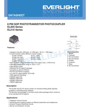
4.1 Pin Configuration
The 8-pin SOP package has the following pinout: Pin 1: Anode, Pin 2: Cathode, Pins 3, 4, 8: No Connection (NC), Pin 5: Emitter, Pin 6: Collector, Pin 7: Base. The base pin is brought out externally, which provides design flexibility. It can be left open for maximum sensitivity, connected to the emitter through a resistor to reduce sensitivity and improve switching speed, or used for feedback in specific configurations.
4.2 Package Dimensions and PCB Layout
The device conforms to the standard SO-8 footprint. The datasheet includes detailed mechanical drawings with dimensions in millimeters. A recommended pad layout for surface-mount assembly is also provided. Following this land pattern is crucial for achieving reliable solder joints and preventing issues like tombstoning during reflow. The package outline ensures compatibility with automated pick-and-place equipment.
5. Soldering and Assembly Guidelines
The absolute maximum rating for soldering temperature is 260°C for 10 seconds. This is a typical rating for lead-free (Pb-free) reflow soldering processes. Standard IPC/JEDEC J-STD-020 guidelines for moisture sensitivity levels (MSL) and reflow profiles should be followed. Devices should be stored in their original moisture-barrier bags until use. If exposed to ambient humidity beyond their MSL rating, baking is required before soldering to prevent "popcorning" damage during reflow.
6. Packaging and Ordering Information
6.1 Model Numbering Rule
The part number follows the format: EL2XX(Y)-V
- XX: Part number (05, 06, 07, 08, 11, 12, 13, 15, 16, 17). Defines the CTR grade.
- Y: Tape and reel option (TA, TB, or none for tube packaging).
- V: Optional suffix indicating VDE safety approval is included.
6.2 Packaging Options
- Tube: 100 units per tube. Suitable for prototyping or low-volume manual assembly.
- Tape and Reel: 2000 units per reel. Designed for high-volume automated assembly lines. The datasheet includes detailed tape and reel specifications (dimensions of pockets, tape width, reel diameter).
6.3 Device Marking
The top of the package is marked with "EL" (manufacturer code), the part number (e.g., 207), a 1-digit year code (Y), and a 2-digit week code (WW). An optional "V" may be present for VDE-approved versions. This marking allows for traceability and verification of the component.
7. Application Design Considerations
7.1 Driving the Input LED
The LED must be driven with a current-limiting resistor. The value is calculated as RLIMIT = (VDRIVE - VF) / IF. Use the maximum VF from the datasheet to ensure the minimum required IF is achieved under all conditions. For digital switching, ensure the drive circuit can provide the necessary IF to achieve the desired output state within the required time, considering the device's switching speed.
7.2 Output Circuit Design
The load resistor (RL) connected between the collector and VCC determines the output voltage swing and switching speed. A smaller RL provides faster switching (due to smaller RC time constant) but results in a smaller output voltage swing and higher power dissipation. A larger RL gives a larger swing but slower speed. The chosen IF and CTR must guarantee that the phototransistor can sink enough current to pull the output voltage below the logic-low threshold of the receiving circuit when on.
7.3 Using the Base Pin
Leaving the base pin (Pin 7) open provides the highest CTR and sensitivity. Connecting a resistor (typically in the range of 100 kΩ to 1 MΩ) between the base and emitter (Pin 5) shunts some of the photogenerated base current, reducing the effective gain (CTR) but significantly improving the switching speed, especially the turn-off time (toff). This is a common trade-off in high-speed digital isolation applications.
7.4 Ensuring Reliable Isolation
To maintain the rated isolation voltage, proper PCB layout is essential. Maintain adequate creepage and clearance distances on the PCB between the input-side and output-side copper traces, as specified by relevant safety standards (e.g., IEC 60950, IEC 60601). The isolation barrier within the component itself is certified, but the PCB layout must not compromise it.
8. Technical Comparison and Selection Guidance
The EL20X/EL21X series differentiates itself with its high 3750Vrms isolation voltage in a standard SO-8 package, which is higher than many basic 4-pin photocouplers. Compared to more advanced digital isolators (which use CMOS technology), phototransistor photocouplers like these are generally slower, have lower CTR, and CTR degrades over time. However, they offer excellent common-mode rejection, simplicity, and robustness for DC and low-frequency AC signal isolation. The key selection criteria are: required isolation voltage, necessary CTR at the operating IF, acceptable switching speed, and operating temperature range.
9. Frequently Asked Questions (FAQ)
9.1 What is the difference between the EL20X and EL21X series?
The EL20X series (EL205-EL208) specifies CTR with both a minimum and maximum value (a "binned" range), offering tighter parameter control. The EL21X series (EL211-EL213) specifies only a minimum CTR value, which may result in a wider distribution of actual values but potentially at a lower cost.
9.2 How does temperature affect performance?
CTR decreases with increasing temperature. For reliable operation over the full temperature range, design calculations should use the minimum expected CTR at the maximum operating temperature. The datasheet typically provides derating curves or a temperature coefficient for this purpose.
9.3 Can this device be used for analog signal isolation?
Yes, but with limitations. The phototransistor's response is non-linear, and CTR varies with IF and temperature. For linear analog isolation, additional external circuitry (operational amplifiers, feedback) is required to linearize the response, or a dedicated linear optocoupler should be considered.
9.4 What is the purpose of the "V" option in the part number?
The "-V" suffix indicates that the specific unit has been tested and certified to meet the VDE (Verband der Elektrotechnik) safety standard for reinforced insulation. This is often a requirement for products sold in the European market.
10. Practical Design Example
Scenario: Isolating a 3.3V microcontroller GPIO pin to control a 12V relay coil on a separate circuit. The relay coil requires 50mA to activate.
Design Steps:
- Interface Selection: Use the photocoupler as a low-side switch for the relay. The microcontroller drives the LED side. The phototransistor will sink the relay coil current.
- Part Selection: Choose a part with sufficient CTR. Required IC = 50mA. If targeting IF = 5mA from the MCU, minimum required CTR = (50mA / 5mA)*100% = 1000%. A standard phototransistor cannot provide this. Therefore, the photocoupler must drive a small transistor (a "post-transistor") which then drives the relay. Select an EL207 (CTR 100-200%) for good gain.
- Input Circuit: MCU GPIO (3.3V) -> Current limiting resistor R1 -> EL207 pins 1 (Anode) and 2 (Cathode). R1 = (3.3V - 1.5V) / 0.005A = 360Ω (use 330Ω standard).
- Output Circuit: 12V supply -> Relay coil -> Collector (Pin 6) of EL207. Emitter (Pin 5) to ground. A flyback diode must be placed in reverse parallel across the relay coil to protect the phototransistor from voltage spikes when it turns off. A base-emitter resistor (e.g., 1 MΩ) can be added to Pin 7 to improve turn-off speed.
- Verification: At IF=5mA, minimum CTR of 100% gives IC = 5mA. This is enough to saturate a small BJT (e.g., 2N3904) with high gain, which can then switch the 50mA relay coil.
11. Operating Principle
A photocoupler consists of two main components housed in a light-tight package. On the input side, an infrared Gallium Arsenide (GaAs) light-emitting diode (LED) converts electrical current into infrared light. The intensity of this light is directly proportional to the forward current (IF) flowing through the LED. This light travels across a transparent isolation gap (often filled with a dielectric gel) and strikes the silicon phototransistor on the output side. The phototransistor's base region is designed to be sensitive to this specific wavelength of light. The incident photons generate electron-hole pairs in the base-collector junction, creating a photocurrent that acts as a base current. This photogenerated base current is then amplified by the transistor's current gain (hFE), resulting in a much larger collector current (IC). The ratio IC/IF is the Current Transfer Ratio (CTR). The key point is that the signal is transferred by light, providing galvanic isolation determined by the physical properties of the internal insulation material and the distance between the LED and the transistor.
12. Technology Trends
Phototransistor-based photocouplers like the EL20X/EL21X represent a mature and reliable isolation technology. Current trends in signal isolation include the growing adoption of digital isolators based on CMOS technology and RF or capacitive coupling. These offer significant advantages in speed (up to hundreds of Mbps), power consumption, size, and longevity (no LED degradation). However, traditional photocouplers maintain strong positions in applications requiring very high isolation voltage (>5kV), excellent common-mode transient immunity (CMTI), simplicity, and cost-effectiveness for DC and low-frequency isolation. There is also ongoing development in photocoupler technology itself, such as integrating the phototransistor with a base-emitter resistor for faster speed (as seen in the availability of the base pin) and developing packages with higher creepage/clearance distances for reinforced isolation requirements.
LED Specification Terminology
Complete explanation of LED technical terms
Photoelectric Performance
| Term | Unit/Representation | Simple Explanation | Why Important |
|---|---|---|---|
| Luminous Efficacy | lm/W (lumens per watt) | Light output per watt of electricity, higher means more energy efficient. | Directly determines energy efficiency grade and electricity cost. |
| Luminous Flux | lm (lumens) | Total light emitted by source, commonly called "brightness". | Determines if the light is bright enough. |
| Viewing Angle | ° (degrees), e.g., 120° | Angle where light intensity drops to half, determines beam width. | Affects illumination range and uniformity. |
| CCT (Color Temperature) | K (Kelvin), e.g., 2700K/6500K | Warmth/coolness of light, lower values yellowish/warm, higher whitish/cool. | Determines lighting atmosphere and suitable scenarios. |
| CRI / Ra | Unitless, 0–100 | Ability to render object colors accurately, Ra≥80 is good. | Affects color authenticity, used in high-demand places like malls, museums. |
| SDCM | MacAdam ellipse steps, e.g., "5-step" | Color consistency metric, smaller steps mean more consistent color. | Ensures uniform color across same batch of LEDs. |
| Dominant Wavelength | nm (nanometers), e.g., 620nm (red) | Wavelength corresponding to color of colored LEDs. | Determines hue of red, yellow, green monochrome LEDs. |
| Spectral Distribution | Wavelength vs intensity curve | Shows intensity distribution across wavelengths. | Affects color rendering and quality. |
Electrical Parameters
| Term | Symbol | Simple Explanation | Design Considerations |
|---|---|---|---|
| Forward Voltage | Vf | Minimum voltage to turn on LED, like "starting threshold". | Driver voltage must be ≥Vf, voltages add up for series LEDs. |
| Forward Current | If | Current value for normal LED operation. | Usually constant current drive, current determines brightness & lifespan. |
| Max Pulse Current | Ifp | Peak current tolerable for short periods, used for dimming or flashing. | Pulse width & duty cycle must be strictly controlled to avoid damage. |
| Reverse Voltage | Vr | Max reverse voltage LED can withstand, beyond may cause breakdown. | Circuit must prevent reverse connection or voltage spikes. |
| Thermal Resistance | Rth (°C/W) | Resistance to heat transfer from chip to solder, lower is better. | High thermal resistance requires stronger heat dissipation. |
| ESD Immunity | V (HBM), e.g., 1000V | Ability to withstand electrostatic discharge, higher means less vulnerable. | Anti-static measures needed in production, especially for sensitive LEDs. |
Thermal Management & Reliability
| Term | Key Metric | Simple Explanation | Impact |
|---|---|---|---|
| Junction Temperature | Tj (°C) | Actual operating temperature inside LED chip. | Every 10°C reduction may double lifespan; too high causes light decay, color shift. |
| Lumen Depreciation | L70 / L80 (hours) | Time for brightness to drop to 70% or 80% of initial. | Directly defines LED "service life". |
| Lumen Maintenance | % (e.g., 70%) | Percentage of brightness retained after time. | Indicates brightness retention over long-term use. |
| Color Shift | Δu′v′ or MacAdam ellipse | Degree of color change during use. | Affects color consistency in lighting scenes. |
| Thermal Aging | Material degradation | Deterioration due to long-term high temperature. | May cause brightness drop, color change, or open-circuit failure. |
Packaging & Materials
| Term | Common Types | Simple Explanation | Features & Applications |
|---|---|---|---|
| Package Type | EMC, PPA, Ceramic | Housing material protecting chip, providing optical/thermal interface. | EMC: good heat resistance, low cost; Ceramic: better heat dissipation, longer life. |
| Chip Structure | Front, Flip Chip | Chip electrode arrangement. | Flip chip: better heat dissipation, higher efficacy, for high-power. |
| Phosphor Coating | YAG, Silicate, Nitride | Covers blue chip, converts some to yellow/red, mixes to white. | Different phosphors affect efficacy, CCT, and CRI. |
| Lens/Optics | Flat, Microlens, TIR | Optical structure on surface controlling light distribution. | Determines viewing angle and light distribution curve. |
Quality Control & Binning
| Term | Binning Content | Simple Explanation | Purpose |
|---|---|---|---|
| Luminous Flux Bin | Code e.g., 2G, 2H | Grouped by brightness, each group has min/max lumen values. | Ensures uniform brightness in same batch. |
| Voltage Bin | Code e.g., 6W, 6X | Grouped by forward voltage range. | Facilitates driver matching, improves system efficiency. |
| Color Bin | 5-step MacAdam ellipse | Grouped by color coordinates, ensuring tight range. | Guarantees color consistency, avoids uneven color within fixture. |
| CCT Bin | 2700K, 3000K etc. | Grouped by CCT, each has corresponding coordinate range. | Meets different scene CCT requirements. |
Testing & Certification
| Term | Standard/Test | Simple Explanation | Significance |
|---|---|---|---|
| LM-80 | Lumen maintenance test | Long-term lighting at constant temperature, recording brightness decay. | Used to estimate LED life (with TM-21). |
| TM-21 | Life estimation standard | Estimates life under actual conditions based on LM-80 data. | Provides scientific life prediction. |
| IESNA | Illuminating Engineering Society | Covers optical, electrical, thermal test methods. | Industry-recognized test basis. |
| RoHS / REACH | Environmental certification | Ensures no harmful substances (lead, mercury). | Market access requirement internationally. |
| ENERGY STAR / DLC | Energy efficiency certification | Energy efficiency and performance certification for lighting. | Used in government procurement, subsidy programs, enhances competitiveness. |