1. Product Overview
The EL3H4-G series is a family of AC input phototransistor photocouplers designed for applications requiring electrical isolation and signal transmission from AC or unknown polarity DC sources. The device is housed in a compact, surface-mount 4-pin Small Outline Package (SSOP), making it suitable for space-constrained PCB designs.
The core component consists of two infrared light-emitting diodes (LEDs) connected in inverse parallel. This configuration allows the input to accept alternating current (AC) signals, as one diode conducts during each half-cycle of the input waveform. The emitted infrared light is optically coupled to a silicon phototransistor, which provides the isolated output signal. The entire assembly is encapsulated with a green, halogen-free compound.
1.1 Core Advantages
- AC Input Capability: The inverse-parallel LED configuration enables direct interfacing with AC signal sources without the need for external rectification circuitry.
- High Isolation Voltage: Provides a safety-rated isolation of 3750 Vrms between the input and output sides, crucial for protecting sensitive circuits from high-voltage transients.
- Compact Form Factor: The SSOP package offers a small footprint, ideal for modern, high-density electronic assemblies.
- Environmental Compliance: The device is halogen-free and complies with relevant environmental directives such as RoHS and REACH.
- Safety Approvals: The product carries approvals from major international safety agencies including UL, cUL, VDE, SEMKO, NEMKO, DEMKO, FIMKO, and CQC.
1.2 Target Applications
This photocoupler is designed for use in a variety of industrial and communication applications where reliable isolation and AC signal detection are required.
- AC Line Monitoring: Detecting the presence or absence of AC mains voltage in power supplies, appliances, and industrial equipment.
- Programmable Logic Controllers (PLCs): Providing isolated digital input channels for sensing AC signals from sensors and switches.
- Telephone Line Interface: Isolating ringing or off-hook detection circuits in telecommunication equipment.
- Unknown Polarity DC Sensing: Interfacing with DC signals where the polarity is not fixed or known in advance.
2. In-Depth Technical Parameter Analysis
2.1 Absolute Maximum Ratings
The Absolute Maximum Ratings define the stress limits beyond which permanent damage to the device may occur. These are not intended for normal operating conditions.
- Input Forward Current (IF): ±50 mA (continuous). The ± sign indicates the AC/ bidirectional capability.
- Peak Forward Current (IFM): 1 A for a short pulse duration of 10 µs. This rating is important for withstanding brief surge currents.
- Collector-Emitter Voltage (VCEO): 80 V. This is the maximum voltage that can be applied across the output phototransistor.
- Total Power Dissipation (PTOT): 200 mW. This is the maximum combined power the device can dissipate from both input and output sides.
- Isolation Voltage (VISO): 3750 Vrms for 1 minute. This high-voltage withstand rating is a key safety parameter.
- Operating Temperature (TOPR): -55°C to +100°C. The wide range ensures reliable operation in harsh environments.
- Soldering Temperature (TSOL): 260°C for 10 seconds, compliant with typical lead-free reflow soldering profiles.
2.2 Electro-Optical Characteristics
These parameters define the electrical and optical performance of the device under specified test conditions (typically at Ta = 25°C).
2.2.1 Input Characteristics
- Forward Voltage (VF): Typically 1.2V, with a maximum of 1.4V at a forward current of ±20 mA. This low voltage drop is beneficial for low-power circuits.
- Input Capacitance (Cin): Typically 50 pF, maximum 250 pF. This parameter affects the high-frequency response of the input side.
2.2.2 Output Characteristics
- Collector-Emitter Dark Current (ICEO): Maximum 100 nA at VCE=20V with IF=0. This is the leakage current of the phototransistor when no light is present.
- Collector-Emitter Breakdown Voltage (BVCEO): Minimum 80V. This ensures the output can handle typical logic or medium voltage levels.
- Collector-Emitter Saturation Voltage (VCE(sat)): Typically 0.1V, maximum 0.2V at IF=±20mA and IC=1mA. A low saturation voltage is desirable for output stages driving logic inputs.
2.2.3 Transfer Characteristics
These parameters define the efficiency and quality of the signal transfer from input to output.
- Current Transfer Ratio (CTR): This is the ratio of output collector current (IC) to input forward current (IF), expressed as a percentage. It is the key parameter for gain. The EL3H4-G series is offered in different CTR ranks:
- EL3H4: CTR min. 20% to max. 300% at IF = ±1 mA, VCE = 5V.
- EL3H4A: CTR min. 50% to max. 150%.
- EL3H4B: CTR min. 100% to max. 300%.
- CTR Symmetry: Ratio of CTR measured with positive IF to CTR measured with negative IF. Specified between 0.5 and 2.0. A value close to 1.0 indicates good symmetry in the AC response of the two input LEDs.
- Isolation Resistance (RIO): Minimum 5×10¹⁰ Ω, typical 1011 Ω at 500V DC. This extremely high resistance is critical for maintaining isolation integrity.
- Floating Capacitance (CIO): Typically 0.6 pF, maximum 1.0 pF. This low capacitance minimizes capacitive coupling across the isolation barrier, which is important for rejecting high-frequency common-mode noise.
- Switching Times: Both rise time (tr) and fall time (tf) have a maximum value of 18 µs under the specified test conditions (VCE=2V, IC=2mA, RL=100Ω). These times define the device's speed and suitability for different frequency signals.
3. Grading System Explanation
The EL3H4-G series employs a grading system primarily based on the Current Transfer Ratio (CTR).
- Standard Grade (No suffix): Offers the widest CTR range (20-300%), suitable for general-purpose applications where precise gain is not critical.
- A Grade (Suffix 'A'): Provides a tighter, mid-range CTR (50-150%), offering more predictable performance.
- B Grade (Suffix 'B'): Provides a tight, high CTR range (100-300%), ideal for applications requiring high sensitivity and gain, such as detecting weak signals.
This binning allows manufacturers to optimize their designs for consistency or to select parts for specific sensitivity requirements.
4. Performance Curve Analysis
The datasheet references typical electro-optical characteristic curves. While the specific graphs are not detailed in the provided text, they typically include the following, which are crucial for design:
- CTR vs. Forward Current (IF): Shows how the transfer ratio changes with the input current level. CTR often decreases at very high IF due to LED efficiency droop.
- CTR vs. Temperature: Illustrates the temperature dependence of the device's sensitivity. CTR generally decreases with increasing temperature.
- Forward Voltage (VF) vs. Forward Current (IF): The diode's IV characteristic curve.
- Output Collector Current (IC) vs. Collector-Emitter Voltage (VCE): The phototransistor's output characteristics for different input light levels (IF).
- Switching Time vs. Load Resistance (RL): Shows how the rise and fall times are affected by the chosen load resistor on the output.
Designers should consult these curves to understand device behavior under non-standard conditions and to optimize parameters like input current and load resistance for desired speed and output swing.
5. Mechanical and Package Information
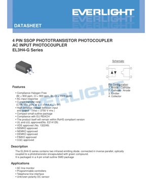
5.1 Pin Configuration
The 4-pin SSOP package has the following pinout:
- Pin 1: Anode of one LED / Cathode of the other (due to inverse-parallel connection).
- Pin 2: Cathode of the first LED / Anode of the second.
- Pin 3: Emitter of the phototransistor.
- Pin 4: Collector of the phototransistor.
This configuration means the AC input is applied between Pins 1 and 2, and the output is taken from Pins 3 and 4 (typically with Pin 3 as common/ground).
5.2 Package Dimensions and PCB Layout
The datasheet includes detailed mechanical drawings for the SSOP package. Key dimensions include the body size, lead pitch, and standoff height. A recommended pad layout for surface mounting is also provided, with the note that it is for reference and should be modified based on specific PCB manufacturing processes and thermal requirements. Proper pad design is essential for reliable soldering and mechanical strength.
6. Soldering and Assembly Guidelines
6.1 Reflow Soldering Profile
The device is compatible with lead-free reflow soldering processes. The recommended maximum body temperature profile is based on IPC/JEDEC J-STD-020D:
- Preheat: 150°C to 200°C over 60-120 seconds.
- Time Above Liquidus (TL=217°C): 60-100 seconds.
- Peak Temperature (TP): 260°C maximum.
- Time within 5°C of Peak: 30 seconds maximum.
- Maximum Reflow Cycles: 3.
Adhering to this profile prevents thermal damage to the plastic package and the internal wire bonds.
6.2 Precautions
- Avoid exposing the device to temperatures exceeding the absolute maximum ratings during handling and soldering.
- Ensure the isolation barrier is not compromised by contamination (e.g., flux, debris) between the input and output sides of the package.
- Follow standard ESD (Electrostatic Discharge) precautions during handling, as the internal LEDs and transistors are sensitive to static electricity.
7. Packaging and Ordering Information
7.1 Model Numbering Rule
The part number follows the format: EL3H4(Y)(Z)-VG
- EL3H4: Base part number.
- Y: CTR Rank (A, B, or blank for standard).
- Z: Tape and Reel option (TA, TB, EA, EB, or blank for tube). TA/TB reels contain 5000 units; EA/EB reels contain 1000 units. The difference between A and B options typically relates to tape width or feed direction.
- V: Optional suffix denoting the part carries VDE approval.
- G: Denotes Halogen-Free material.
Example: EL3H4A-TA-VG is an 'A' grade part, supplied on a 5000-unit TA reel, with VDE approval, and is halogen-free.
7.2 Packaging Specifications
The device can be supplied in tubes (150 units) or on tape and reel. Detailed tape dimensions (pocket size, pitch, tape width) are provided for compatibility with automated pick-and-place equipment.
7.3 Device Marking
The top of the package is marked with a code: EL 3H4 RYWWV
- EL: Manufacturer code.
- 3H4: Device number.
- R: CTR Rank (A, B, or blank).
- Y: 1-digit year code.
- WW: 2-digit week code.
- V: VDE approval mark (if present).
8. Application Design Considerations
8.1 Input Circuit Design
For AC operation, a current-limiting resistor must be placed in series with the input pins (1 and 2). Its value should be calculated based on the peak input voltage and the desired forward current (IF), ensuring IF does not exceed the continuous rating of 50 mA. For example, to drive the input from a 120Vrms AC line, the resistor must limit the peak current (≈170V / R). Consider power rating and voltage withstand capability of this resistor.
8.2 Output Circuit Design
The output phototransistor can be used in a common-emitter configuration (load resistor between VCC and Collector, Emitter to ground) or as a switch. The value of the load resistor (RL) affects:
Output Voltage Swing: Higher RL gives a larger voltage drop for a given IC.
Switching Speed: Higher RL increases the RC time constant, slowing down the rise and fall times (as indicated by the tr/tf specification with RL=100Ω).
A pull-up resistor is often needed if driving a logic input. Ensure the output voltage in the 'on' state (VCE(sat)) is low enough to be recognized as a logic '0'.
8.3 Ensuring Reliable Isolation
To maintain the specified 3750Vrms isolation, PCB layout is critical. Maintain adequate creepage and clearance distances on the board between the copper traces and pads associated with the input side (Pins 1,2) and the output side (Pins 3,4). This often means providing a physical slot or wide separation in the PCB under the device body. Avoid running input and output traces in parallel close to each other.
9. Technical Comparison and Differentiation
The primary differentiating features of the EL3H4-G series compared to standard DC-input photocouplers are:
- Built-in AC Input: Eliminates the need for external bridge rectifiers or dual photocouplers to handle AC signals, saving board space and component count.
- CTR Symmetry: A specified parameter ensuring balanced response on both AC half-cycles, which is not a concern for DC-input devices.
- Halogen-Free Construction: Meets stringent environmental requirements that may not be addressed by all older photocoupler models.
Compared to other AC input photocouplers, its advantages lie in the combination of high isolation voltage, compact SSOP package, and availability of multiple CTR grades.
10. Frequently Asked Questions (Based on Technical Parameters)
Q1: Can I use this to directly sense 230V AC mains?
A: Yes, but you must use an appropriate external current-limiting resistor in series with the input to keep the forward current within the 50mA limit. The resistor must also be rated for the high voltage and power dissipation.
Q2: What is the difference between the standard, A, and B grades?
A: The difference is the guaranteed minimum and maximum Current Transfer Ratio (CTR). The B grade has the highest minimum sensitivity (100%), making it suitable for detecting weaker signals. The A grade offers a more moderate, predictable range. The standard grade has the widest range, offering cost-effective general-purpose use.
Q3: How fast is this device? Can it be used for communication?
A: With typical rise/fall times of up to 18 µs, the bandwidth is limited to roughly tens of kHz. It is suitable for detecting AC power frequency (50/60 Hz), slow digital signals, or state detection in PLCs, but it is not designed for high-speed data communication like digital isolators.
Q4: Why is the isolation resistance so high (10^11 Ω)?
A: This extremely high resistance minimizes leakage current across the isolation barrier. This is crucial for safety, preventing dangerous currents from flowing between isolated circuits, and for signal integrity in precision measurement applications.
11. Practical Design Example
Scenario: Isolated 120V AC Line Presence Detector.
Goal: Provide a 3.3V logic-low signal to a microcontroller when 120V AC is present.
Design Steps:
1. Input Resistor Calculation: For 120Vrms, peak voltage is ~170V. To limit IF to a safe 10mA (well below 50mA), Rlimit = 170V / 0.01A = 17kΩ. Use a standard 18kΩ, 1/2W or higher rated resistor.
2. Output Circuit: Connect the phototransistor Collector (Pin 4) to the microcontroller's 3.3V supply via a pull-up resistor (e.g., 10kΩ). Connect the Emitter (Pin 3) to ground. The Collector node connects to a digital input pin on the microcontroller.
3. Operation: When AC is present, the photocoupler's output turns on during each half-cycle, pulling the Collector voltage down close to VCE(sat) (~0.2V), which is read as a logic '0'. When AC is absent, the phototransistor is off, and the pull-up resistor brings the Collector voltage to 3.3V (logic '1'). Software may need to debounce this signal due to the 50/60 Hz zero-crossings.
12. Operating Principle
The EL3H4-G operates on the principle of optoelectronic coupling. An electrical signal applied to the input side causes the infrared LEDs to emit light proportional to the current. This light traverses a transparent isolation barrier within the package. On the output side, the light strikes the base region of a silicon phototransistor, generating electron-hole pairs. This photocurrent acts as base current, causing the transistor to conduct a much larger collector current, thereby replicating the input signal on the isolated output side. The inverse-parallel LED configuration allows current to flow and light to be emitted during both polarities of an AC input signal.
13. Technology Trends
Photocouplers like the EL3H4-G represent a mature and reliable isolation technology. Current trends in the field of signal isolation include:
Integration: Combining multiple isolation channels or integrating additional functions (like drivers or protection) into a single package.
Higher Speed: Development of photocouplers with faster switching times for digital communication applications, though they are generally slower than technologies based on capacitive or magnetic coupling.
Enhanced Safety Standards: Continuous evolution of international safety standards (UL, VDE, IEC) driving requirements for higher working voltages, reinforced isolation, and improved reliability metrics.
Material Science: Development of new encapsulation compounds with better thermal stability, moisture resistance, and optical clarity to improve performance and longevity.
LED Specification Terminology
Complete explanation of LED technical terms
Photoelectric Performance
| Term | Unit/Representation | Simple Explanation | Why Important |
|---|---|---|---|
| Luminous Efficacy | lm/W (lumens per watt) | Light output per watt of electricity, higher means more energy efficient. | Directly determines energy efficiency grade and electricity cost. |
| Luminous Flux | lm (lumens) | Total light emitted by source, commonly called "brightness". | Determines if the light is bright enough. |
| Viewing Angle | ° (degrees), e.g., 120° | Angle where light intensity drops to half, determines beam width. | Affects illumination range and uniformity. |
| CCT (Color Temperature) | K (Kelvin), e.g., 2700K/6500K | Warmth/coolness of light, lower values yellowish/warm, higher whitish/cool. | Determines lighting atmosphere and suitable scenarios. |
| CRI / Ra | Unitless, 0–100 | Ability to render object colors accurately, Ra≥80 is good. | Affects color authenticity, used in high-demand places like malls, museums. |
| SDCM | MacAdam ellipse steps, e.g., "5-step" | Color consistency metric, smaller steps mean more consistent color. | Ensures uniform color across same batch of LEDs. |
| Dominant Wavelength | nm (nanometers), e.g., 620nm (red) | Wavelength corresponding to color of colored LEDs. | Determines hue of red, yellow, green monochrome LEDs. |
| Spectral Distribution | Wavelength vs intensity curve | Shows intensity distribution across wavelengths. | Affects color rendering and quality. |
Electrical Parameters
| Term | Symbol | Simple Explanation | Design Considerations |
|---|---|---|---|
| Forward Voltage | Vf | Minimum voltage to turn on LED, like "starting threshold". | Driver voltage must be ≥Vf, voltages add up for series LEDs. |
| Forward Current | If | Current value for normal LED operation. | Usually constant current drive, current determines brightness & lifespan. |
| Max Pulse Current | Ifp | Peak current tolerable for short periods, used for dimming or flashing. | Pulse width & duty cycle must be strictly controlled to avoid damage. |
| Reverse Voltage | Vr | Max reverse voltage LED can withstand, beyond may cause breakdown. | Circuit must prevent reverse connection or voltage spikes. |
| Thermal Resistance | Rth (°C/W) | Resistance to heat transfer from chip to solder, lower is better. | High thermal resistance requires stronger heat dissipation. |
| ESD Immunity | V (HBM), e.g., 1000V | Ability to withstand electrostatic discharge, higher means less vulnerable. | Anti-static measures needed in production, especially for sensitive LEDs. |
Thermal Management & Reliability
| Term | Key Metric | Simple Explanation | Impact |
|---|---|---|---|
| Junction Temperature | Tj (°C) | Actual operating temperature inside LED chip. | Every 10°C reduction may double lifespan; too high causes light decay, color shift. |
| Lumen Depreciation | L70 / L80 (hours) | Time for brightness to drop to 70% or 80% of initial. | Directly defines LED "service life". |
| Lumen Maintenance | % (e.g., 70%) | Percentage of brightness retained after time. | Indicates brightness retention over long-term use. |
| Color Shift | Δu′v′ or MacAdam ellipse | Degree of color change during use. | Affects color consistency in lighting scenes. |
| Thermal Aging | Material degradation | Deterioration due to long-term high temperature. | May cause brightness drop, color change, or open-circuit failure. |
Packaging & Materials
| Term | Common Types | Simple Explanation | Features & Applications |
|---|---|---|---|
| Package Type | EMC, PPA, Ceramic | Housing material protecting chip, providing optical/thermal interface. | EMC: good heat resistance, low cost; Ceramic: better heat dissipation, longer life. |
| Chip Structure | Front, Flip Chip | Chip electrode arrangement. | Flip chip: better heat dissipation, higher efficacy, for high-power. |
| Phosphor Coating | YAG, Silicate, Nitride | Covers blue chip, converts some to yellow/red, mixes to white. | Different phosphors affect efficacy, CCT, and CRI. |
| Lens/Optics | Flat, Microlens, TIR | Optical structure on surface controlling light distribution. | Determines viewing angle and light distribution curve. |
Quality Control & Binning
| Term | Binning Content | Simple Explanation | Purpose |
|---|---|---|---|
| Luminous Flux Bin | Code e.g., 2G, 2H | Grouped by brightness, each group has min/max lumen values. | Ensures uniform brightness in same batch. |
| Voltage Bin | Code e.g., 6W, 6X | Grouped by forward voltage range. | Facilitates driver matching, improves system efficiency. |
| Color Bin | 5-step MacAdam ellipse | Grouped by color coordinates, ensuring tight range. | Guarantees color consistency, avoids uneven color within fixture. |
| CCT Bin | 2700K, 3000K etc. | Grouped by CCT, each has corresponding coordinate range. | Meets different scene CCT requirements. |
Testing & Certification
| Term | Standard/Test | Simple Explanation | Significance |
|---|---|---|---|
| LM-80 | Lumen maintenance test | Long-term lighting at constant temperature, recording brightness decay. | Used to estimate LED life (with TM-21). |
| TM-21 | Life estimation standard | Estimates life under actual conditions based on LM-80 data. | Provides scientific life prediction. |
| IESNA | Illuminating Engineering Society | Covers optical, electrical, thermal test methods. | Industry-recognized test basis. |
| RoHS / REACH | Environmental certification | Ensures no harmful substances (lead, mercury). | Market access requirement internationally. |
| ENERGY STAR / DLC | Energy efficiency certification | Energy efficiency and performance certification for lighting. | Used in government procurement, subsidy programs, enhances competitiveness. |