Table of Contents
- 1. Product Overview
- 2. Technical Parameter Deep-Dive
- 2.1 Photometric & Optical Characteristics
- 2.2 Electrical Parameters
- 2.3 Thermal & Reliability Ratings
- 3. Binning System Explanation
- 3.1 Luminous Flux Binning
- 3.2 Forward Voltage Binning
- 3.3 Dominant Wavelength Binning
- 4. Performance Curve Analysis
- 4.1 IV Curve and Relative Luminous Flux
- 4.2 Temperature Dependence
- 4.3 Spectral Distribution and Derating
- 5. Mechanical & Package Information
- 6. Soldering & Assembly Guidelines
- 7. Packaging & Ordering Information
- 8. Application Suggestions
- 8.1 Typical Application Scenarios
- 8.2 Design Considerations
- 9. Technical Comparison & Differentiation
- 10. Frequently Asked Questions (Based on Technical Parameters)
- 11. Practical Design Case Study
- 12. Operating Principle Introduction
- 13. Technology Trends
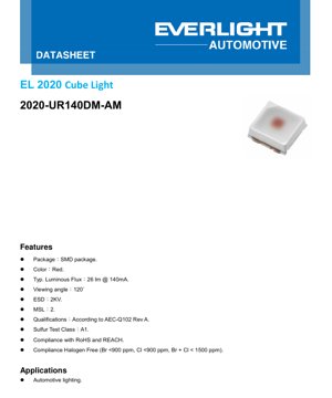
1. Product Overview
This document details the specifications for the 2020 Cube Light, a high-brightness red Surface-Mount Device (SMD) LED engineered primarily for demanding automotive lighting environments. The component is characterized by its compact 2020 footprint, robust construction, and performance parameters tailored for reliability under harsh operating conditions. Its core advantages include compliance with stringent automotive qualification standards, a wide viewing angle for uniform illumination, and environmental compliance certifications.
The primary target market is the automotive industry, where it is suitable for various interior and exterior signal lighting functions. The design prioritizes long-term stability, thermal performance, and resistance to environmental stressors commonly encountered in vehicle applications.
2. Technical Parameter Deep-Dive
2.1 Photometric & Optical Characteristics
The LED's key photometric performance is defined at a standard test current of 140mA. The typical luminous flux output is 26 lumens (lm), with a specified minimum of 23 lm and a maximum of 39 lm, accounting for production binning. The dominant wavelength is typically 614 nm, placing it firmly in the red spectrum, with a range from 612 nm to 627 nm. A wide 120-degree viewing angle (with a ±5° tolerance) ensures a broad radiation pattern, which is beneficial for applications requiring wide-area illumination or visibility from multiple angles.
2.2 Electrical Parameters
The forward voltage (Vf) at the 140mA test condition has a typical value of 2.2V, ranging from a minimum of 1.75V to a maximum of 2.75V. The absolute maximum continuous forward current is rated at 250 mA. For surge conditions (pulse width ≤10 μs, duty cycle 0.005), the device can withstand a surge current (IFM) of up to 1000 mA. It is crucial to note that this LED is not designed for reverse bias operation.
2.3 Thermal & Reliability Ratings
Thermal management is critical for LED longevity. The junction-to-solder point thermal resistance is specified with two values: an electrical method result of 16-18 K/W and a real method result of 23-26 K/W. The maximum permissible junction temperature (Tj) is 150°C. The device is rated for an operating temperature range of -40°C to +125°C, matching the extremes required for automotive use. It features Electrostatic Discharge (ESD) protection rated at 2 kV (Human Body Model). The component is also qualified for lead-free reflow soldering with a peak temperature of 260°C for 30 seconds.
3. Binning System Explanation
To ensure consistency in production, LEDs are sorted into performance bins. Understanding these bins is essential for design consistency.
3.1 Luminous Flux Binning
LEDs are grouped based on their light output at 140mA. The primary bins are E9 (23-27 lm), F1 (27-33 lm), and F2 (33-39 lm). The typical value of 26 lm falls within the E9 bin.
3.2 Forward Voltage Binning
Components are also binned according to their forward voltage drop. Key bins include 1720 (1.75-2.0V), 2022 (2.0-2.25V), 2225 (2.25-2.5V), and 2527 (2.5-2.75V). The typical 2.2V value corresponds to the 2022 bin.
3.3 Dominant Wavelength Binning
The color (wavelength) is tightly controlled through bins such as 1215 (612-615 nm), 1518 (615-618 nm), up to 2427 (624-627 nm). The typical 614 nm is in the 1215 bin.
4. Performance Curve Analysis
4.1 IV Curve and Relative Luminous Flux
The Forward Current vs. Forward Voltage graph shows a characteristic exponential relationship. The Relative Luminous Flux vs. Forward Current curve indicates that light output increases with current but will eventually saturate and can degrade efficiency and lifetime at higher currents beyond recommendation.
4.2 Temperature Dependence
The Relative Luminous Flux vs. Junction Temperature graph is critical for thermal design. It shows that light output decreases as junction temperature increases. The Dominant Wavelength Shift vs. Junction Temperature graph indicates the color will shift (typically towards longer wavelengths) as temperature rises, which must be considered in color-critical applications.
4.3 Spectral Distribution and Derating
The Relative Spectral Distribution graph confirms a narrow-band red emission peak. The Forward Current Derating Curve mandates reducing the maximum allowable continuous current as the solder pad temperature increases to prevent exceeding the maximum junction temperature. For example, at a pad temperature of 125°C, the current must be derated to 250 mA.
5. Mechanical & Package Information
The component uses a standard 2020 SMD package (2.0mm x 2.0mm footprint). The mechanical drawing specifies the exact dimensions, including overall height, lead frame details, and lens geometry. Tolerances are typically ±0.1mm unless otherwise noted. A recommended soldering pad layout is provided to ensure proper solder joint formation, thermal transfer, and mechanical stability during reflow and operation. The polarity is indicated by a specific marking or pin configuration on the component body, which must be observed during placement.
6. Soldering & Assembly Guidelines
The LED is compatible with standard lead-free reflow soldering processes. A detailed reflow soldering profile is provided, specifying the critical parameters: preheat slope, soak time and temperature, time above liquidus (TAL), peak temperature (260°C max for 30 seconds), and cooling rate. Adherence to this profile is essential to prevent thermal shock, solder joint defects, or damage to the LED package. General precautions include using appropriate ESD protection during handling, avoiding mechanical stress on the lens, and ensuring the soldering environment is free from contaminants like sulfur.
7. Packaging & Ordering Information
The parts are supplied in standard tape-and-reel packaging suitable for automated pick-and-place assembly machines. The packaging information details reel dimensions, pocket spacing, and orientation. The part number follows a specific structure: 2020 - UR - 140 - D - M - AM.
- 2020: Product family.
- UR: Color (Red).
- 140: Test Current in mA.
- D: Lead Frame Type (Au + White glue).
- M: Brightness Level (Medium).
- AM: Automotive application designation.
8. Application Suggestions
8.1 Typical Application Scenarios
The primary application is automotive lighting. This includes, but is not limited to, center high-mount stop lights (CHMSL), rear combination lamps (tail/stop lights), side marker lights, and interior ambient lighting. Its AEC-Q102 qualification and wide temperature range make it suitable for these harsh environments.
8.2 Design Considerations
Driver Circuit: A constant-current driver is strongly recommended to ensure stable light output and prevent thermal runaway, as LED forward voltage has a negative temperature coefficient.
Thermal Management: The PCB layout must facilitate heat dissipation. Use the recommended solder pad design, ensure adequate copper area connected to the thermal pad, and consider the overall system thermal path to keep the solder pad temperature within safe limits for the desired operating current.
Optical Design: The 120° viewing angle may require secondary optics (lenses, light guides) to shape the beam for specific applications. The potential for wavelength shift with temperature should be evaluated for color-sensitive uses.
9. Technical Comparison & Differentiation
Compared to generic commercial-grade LEDs, this component's key differentiators are its automotive-grade qualifications (AEC-Q102), extended operating temperature range (-40°C to +125°C), and specific reliability testing (e.g., Sulfur Test Class A1). It also complies with Halogen-Free requirements, which is increasingly important for environmental and reliability reasons in automotive electronics. The combination of a medium brightness level (26 lm typ) with robust construction offers a balanced solution for applications where reliability is prioritized over ultimate brightness.
10. Frequently Asked Questions (Based on Technical Parameters)
Q: Can I drive this LED at its absolute maximum current of 250mA continuously?
A: Not necessarily. The 250mA rating is the absolute maximum under specific conditions. The safe continuous operating current depends on the thermal design. You must use the forward current derating curve based on your measured or estimated solder pad temperature (Ts). For example, if Ts is 100°C, the maximum allowed continuous current is significantly lower than 250mA.
Q: What is the difference between the real and electrical thermal resistance (Rth JS)?
A: The electrical method uses the LED's temperature-sensitive electrical parameters to estimate junction temperature, while the real method may use a physical sensor. The real method value (23-26 K/W) is generally considered more conservative and reliable for thermal design calculations.
Q: The datasheet mentions a Sulfur Test. Why is this important?
A: Sulfur-containing atmospheres (e.g., from certain rubbers, gaskets, or industrial environments) can corrode silver-based lead frames, leading to failure. A Sulfur Test Class A1 rating indicates the device has passed specific testing for resistance to sulfur corrosion, which is crucial for long-term reliability in enclosed automotive assemblies.
11. Practical Design Case Study
Consider designing a rear stop light module using this LED. A cluster of 10 LEDs in series would require a driver capable of providing 140mA at approximately 22V (10 * 2.2V typical), plus headroom. The PCB must be designed with thermal vias under each LED's thermal pad, connecting to a large internal ground plane for heat spreading. The derating curve must be consulted: if the PCB's temperature near the LEDs reaches 80°C in the worst-case ambient environment, the maximum permissible current per LED must be checked and potentially reduced from 140mA to ensure the junction temperature stays below 150°C. Optical simulation would be used to arrange the LEDs and design a diffuser to meet the required luminous intensity distribution and uniformity standards for automotive stop lights.
12. Operating Principle Introduction
This is a semiconductor-based light-emitting diode. When a forward voltage exceeding its characteristic forward voltage (Vf) is applied, electrons and holes recombine within the active region of the semiconductor chip, releasing energy in the form of photons (light). The specific material composition of the semiconductor (likely based on AlInGaP for red emission) determines the dominant wavelength of the emitted light. The SMD package incorporates a lead frame for electrical connection and thermal conduction, a silicone lens to protect the chip and shape the light output, and a white reflective cavity to enhance light extraction efficiency.
13. Technology Trends
The trend in automotive LED lighting continues towards higher efficiency (more lumens per watt), greater power density, and improved reliability. This allows for smaller, more energy-efficient lighting modules. There is also a focus on advanced functionalities like adaptive driving beams (ADB) and communication via light (Li-Fi), though these typically require more complex components. For standard signaling functions, the emphasis remains on cost-optimized, highly reliable, and qualified components like the one described, with ongoing improvements in thermal performance and lifetime under high-temperature operation.
LED Specification Terminology
Complete explanation of LED technical terms
Photoelectric Performance
| Term | Unit/Representation | Simple Explanation | Why Important |
|---|---|---|---|
| Luminous Efficacy | lm/W (lumens per watt) | Light output per watt of electricity, higher means more energy efficient. | Directly determines energy efficiency grade and electricity cost. |
| Luminous Flux | lm (lumens) | Total light emitted by source, commonly called "brightness". | Determines if the light is bright enough. |
| Viewing Angle | ° (degrees), e.g., 120° | Angle where light intensity drops to half, determines beam width. | Affects illumination range and uniformity. |
| CCT (Color Temperature) | K (Kelvin), e.g., 2700K/6500K | Warmth/coolness of light, lower values yellowish/warm, higher whitish/cool. | Determines lighting atmosphere and suitable scenarios. |
| CRI / Ra | Unitless, 0–100 | Ability to render object colors accurately, Ra≥80 is good. | Affects color authenticity, used in high-demand places like malls, museums. |
| SDCM | MacAdam ellipse steps, e.g., "5-step" | Color consistency metric, smaller steps mean more consistent color. | Ensures uniform color across same batch of LEDs. |
| Dominant Wavelength | nm (nanometers), e.g., 620nm (red) | Wavelength corresponding to color of colored LEDs. | Determines hue of red, yellow, green monochrome LEDs. |
| Spectral Distribution | Wavelength vs intensity curve | Shows intensity distribution across wavelengths. | Affects color rendering and quality. |
Electrical Parameters
| Term | Symbol | Simple Explanation | Design Considerations |
|---|---|---|---|
| Forward Voltage | Vf | Minimum voltage to turn on LED, like "starting threshold". | Driver voltage must be ≥Vf, voltages add up for series LEDs. |
| Forward Current | If | Current value for normal LED operation. | Usually constant current drive, current determines brightness & lifespan. |
| Max Pulse Current | Ifp | Peak current tolerable for short periods, used for dimming or flashing. | Pulse width & duty cycle must be strictly controlled to avoid damage. |
| Reverse Voltage | Vr | Max reverse voltage LED can withstand, beyond may cause breakdown. | Circuit must prevent reverse connection or voltage spikes. |
| Thermal Resistance | Rth (°C/W) | Resistance to heat transfer from chip to solder, lower is better. | High thermal resistance requires stronger heat dissipation. |
| ESD Immunity | V (HBM), e.g., 1000V | Ability to withstand electrostatic discharge, higher means less vulnerable. | Anti-static measures needed in production, especially for sensitive LEDs. |
Thermal Management & Reliability
| Term | Key Metric | Simple Explanation | Impact |
|---|---|---|---|
| Junction Temperature | Tj (°C) | Actual operating temperature inside LED chip. | Every 10°C reduction may double lifespan; too high causes light decay, color shift. |
| Lumen Depreciation | L70 / L80 (hours) | Time for brightness to drop to 70% or 80% of initial. | Directly defines LED "service life". |
| Lumen Maintenance | % (e.g., 70%) | Percentage of brightness retained after time. | Indicates brightness retention over long-term use. |
| Color Shift | Δu′v′ or MacAdam ellipse | Degree of color change during use. | Affects color consistency in lighting scenes. |
| Thermal Aging | Material degradation | Deterioration due to long-term high temperature. | May cause brightness drop, color change, or open-circuit failure. |
Packaging & Materials
| Term | Common Types | Simple Explanation | Features & Applications |
|---|---|---|---|
| Package Type | EMC, PPA, Ceramic | Housing material protecting chip, providing optical/thermal interface. | EMC: good heat resistance, low cost; Ceramic: better heat dissipation, longer life. |
| Chip Structure | Front, Flip Chip | Chip electrode arrangement. | Flip chip: better heat dissipation, higher efficacy, for high-power. |
| Phosphor Coating | YAG, Silicate, Nitride | Covers blue chip, converts some to yellow/red, mixes to white. | Different phosphors affect efficacy, CCT, and CRI. |
| Lens/Optics | Flat, Microlens, TIR | Optical structure on surface controlling light distribution. | Determines viewing angle and light distribution curve. |
Quality Control & Binning
| Term | Binning Content | Simple Explanation | Purpose |
|---|---|---|---|
| Luminous Flux Bin | Code e.g., 2G, 2H | Grouped by brightness, each group has min/max lumen values. | Ensures uniform brightness in same batch. |
| Voltage Bin | Code e.g., 6W, 6X | Grouped by forward voltage range. | Facilitates driver matching, improves system efficiency. |
| Color Bin | 5-step MacAdam ellipse | Grouped by color coordinates, ensuring tight range. | Guarantees color consistency, avoids uneven color within fixture. |
| CCT Bin | 2700K, 3000K etc. | Grouped by CCT, each has corresponding coordinate range. | Meets different scene CCT requirements. |
Testing & Certification
| Term | Standard/Test | Simple Explanation | Significance |
|---|---|---|---|
| LM-80 | Lumen maintenance test | Long-term lighting at constant temperature, recording brightness decay. | Used to estimate LED life (with TM-21). |
| TM-21 | Life estimation standard | Estimates life under actual conditions based on LM-80 data. | Provides scientific life prediction. |
| IESNA | Illuminating Engineering Society | Covers optical, electrical, thermal test methods. | Industry-recognized test basis. |
| RoHS / REACH | Environmental certification | Ensures no harmful substances (lead, mercury). | Market access requirement internationally. |
| ENERGY STAR / DLC | Energy efficiency certification | Energy efficiency and performance certification for lighting. | Used in government procurement, subsidy programs, enhances competitiveness. |