Table of Contents
- 1. Product Overview
- 2. Technical Parameters Deep Objective Interpretation
- 2.1 Absolute Maximum Ratings
- 2.2 Electro-Optical Characteristics
- 3. Binning System Explanation The part number HIR25-21C/L423/TR8 incorporates a binning structure to ensure consistent performance. While the datasheet provides a general device selection guide indicating GaAlAs chip material and water-clear lens, specific bins for parameters like peak wavelength (HUE) and radiant intensity (CAT) are managed during production. Customers receive parts within specified tolerance ranges for these key parameters, guaranteeing the device will perform as required in their specific circuit and application. The 'L423' and 'TR8' codes within the part number relate to specific performance bins and tape/reel packaging specifications, respectively. 4. Performance Curve Analysis
- 4.1 Forward Current vs. Forward Voltage (I-V Curve)
- 4.2 Radiant Intensity vs. Forward Current
- 4.3 Radiant Intensity vs. Ambient Temperature
- 4.4 Spectral Distribution
- 5. Mechanical and Packaging Information
- 5.1 Package Dimensions
- 5.2 Recommended Pad Layout
- 5.3 Carrier Taping Dimensions
- 6. Soldering and Assembly Guidelines
- 6.1 Moisture Sensitivity and Storage
- 6.2 Reflow Soldering Profile
- 6.3 Hand Soldering and Rework
- 7. Packaging and Ordering Information
- 8. Application Suggestions
- 8.1 Typical Application Circuits
- 8.2 Design Considerations
- 9. Technical Comparison and Differentiation
- 10. Frequently Asked Questions (Based on Technical Parameters)
- 11. Practical Use Case Examples
- 12. Principle of Operation Introduction
- 13. Technology Trends and Developments
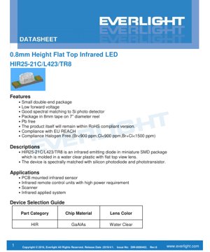
1. Product Overview
The HIR25-21C/L423/TR8 is a miniature surface-mount device (SMD) infrared emitting diode. It is housed in a compact, double-ended package with an exceptionally low profile of 0.8mm, making it suitable for space-constrained applications. The device is molded in water-clear plastic with a flat top lens, which provides a specific radiation pattern. Its core semiconductor material is Gallium Aluminum Arsenide (GaAlAs), engineered for optimal spectral matching with silicon photodiodes and phototransistors, ensuring high efficiency in detection systems.
The product is designed with a low forward voltage characteristic, contributing to overall system power efficiency. It is fully compliant with modern environmental and safety standards, including being lead-free (Pb-free), adhering to the EU REACH regulation, and meeting halogen-free requirements (Br<900 ppm, Cl<900 ppm, Br+Cl<1500 ppm). The device is supplied on 8mm tape mounted on 7-inch diameter reels, facilitating automated assembly processes.
2. Technical Parameters Deep Objective Interpretation
2.1 Absolute Maximum Ratings
The device's operational limits are defined under ambient temperature (Ta) conditions of 25°C. Exceeding these ratings may cause permanent damage. The reverse voltage (VR) is specified at 5V. The forward current (IF) has a maximum rating of 100mA. The power dissipation (PD) is rated at 100mW. The operating temperature range is from -40°C to +85°C, while the storage temperature range extends from -40°C to +100°C. The soldering temperature must be managed carefully, with a peak of 260°C for 10 seconds as per the lead-free reflow profile.
2.2 Electro-Optical Characteristics
The key performance parameters are typically measured at IF=20mA and Ta=25°C. The forward voltage (VF) is typically 1.35V. The radiant intensity (Ie) is specified with a minimum value, defining the optical output power. The peak emission wavelength (λp) is centered in the infrared spectrum, typically around 940nm, which aligns perfectly with the peak sensitivity of common silicon-based receivers. The spectral bandwidth (half-width) is also defined, indicating the range of wavelengths emitted. The viewing angle is determined by the flat-top lens design, providing a specific radiation pattern suitable for targeted applications.
3. Binning System Explanation
The part number HIR25-21C/L423/TR8 incorporates a binning structure to ensure consistent performance. While the datasheet provides a general device selection guide indicating GaAlAs chip material and water-clear lens, specific bins for parameters like peak wavelength (HUE) and radiant intensity (CAT) are managed during production. Customers receive parts within specified tolerance ranges for these key parameters, guaranteeing the device will perform as required in their specific circuit and application. The 'L423' and 'TR8' codes within the part number relate to specific performance bins and tape/reel packaging specifications, respectively.
4. Performance Curve Analysis
The datasheet includes several characteristic curves that provide deeper insight into device behavior beyond the tabular data.
4.1 Forward Current vs. Forward Voltage (I-V Curve)
This curve illustrates the relationship between the current flowing through the LED and the voltage across its terminals. It typically shows an exponential relationship, with a defined "knee" voltage. The low forward voltage characteristic of this LED is visually confirmed here, showing that it begins to conduct significantly at a lower voltage compared to some alternatives, which is beneficial for low-voltage circuit designs.
4.2 Radiant Intensity vs. Forward Current
This graph shows the optical output (radiant intensity) as a function of the drive current. It typically demonstrates a linear relationship within the recommended operating current range, confirming that light output is directly proportional to current. This linearity is crucial for applications requiring modulated signals, such as in infrared data transmission.
4.3 Radiant Intensity vs. Ambient Temperature
This curve depicts how the optical output power decreases as the ambient temperature increases. Like all LEDs, the efficiency of this infrared emitter drops with rising temperature. Understanding this derating is critical for designing systems that operate reliably over the full temperature range, especially in high-temperature environments. Adequate thermal management may be necessary in high-power or high-temperature applications to maintain consistent output.
4.4 Spectral Distribution
A spectral distribution graph shows the relative radiant power emitted across different wavelengths. It will display a clear peak at the nominal wavelength (e.g., 940nm) with a characteristic shape and half-width. This visual confirms the good spectral matching to silicon photodetectors, whose responsivity curve peaks in the same near-infrared region.
5. Mechanical and Packaging Information
5.1 Package Dimensions
The LED has a very compact footprint. The package dimensions are 2.0mm in length, 1.25mm in width, and 0.8mm in height (nominal values). Detailed mechanical drawings provide all critical dimensions including lead spacing, pad positions, and lens geometry. Tolerances for most dimensions are ±0.1mm unless otherwise specified. The anode and cathode are clearly marked on the package for correct polarity identification during assembly.
5.2 Recommended Pad Layout
A suggested land pattern (footprint) for PCB design is provided. This includes the pad size and spacing recommendations to ensure reliable soldering and mechanical stability. The datasheet explicitly notes that this is for reference only, and designers should modify the pad dimensions based on their specific PCB manufacturing capabilities and application requirements, such as thermal or mechanical stress considerations.
5.3 Carrier Taping Dimensions
The device is supplied in embossed carrier tape for automated pick-and-place assembly. The tape width is 8mm. Detailed dimensions for the pocket cavity that holds the LED, the spacing between pockets (pitch), and the positioning of sprocket holes are provided. Each reel contains 2000 pieces (PCS).
6. Soldering and Assembly Guidelines
6.1 Moisture Sensitivity and Storage
The LEDs are packaged in a moisture-proof bag with desiccant. The bag should not be opened until the components are ready for use. After opening, the LEDs should be stored at 30°C or less and 60% relative humidity or less. They must be used within 168 hours (7 days) of opening the bag. If the storage time is exceeded or the desiccant indicates moisture absorption, a baking treatment at 60 ± 5°C for 24 hours is required before use to prevent "popcorning" during reflow soldering.
6.2 Reflow Soldering Profile
A lead-free reflow soldering temperature profile is recommended. Key parameters include a preheat stage, a gradual ramp-up, a peak temperature not exceeding 260°C, and a time above liquidus (typically 217°C) of 30-60 seconds. The peak temperature should be maintained for a maximum of 10 seconds. Reflow soldering should not be performed more than two times on the same device to avoid thermal damage to the plastic package and the semiconductor die.
6.3 Hand Soldering and Rework
If hand soldering is necessary, extreme care must be taken. The soldering iron tip temperature should be below 350°C, and contact time per terminal should be limited to 3 seconds or less. A low-power iron (25W or less) is recommended. A cooling interval of at least 2 seconds should be allowed between soldering the two terminals. Repair after soldering is strongly discouraged. If unavoidable, a specialized double-head soldering iron should be used to simultaneously heat both terminals, preventing thermal stress from lifting one pad while the other is still soldered. The potential for damage during rework is high and should be evaluated beforehand.
7. Packaging and Ordering Information
The standard packaging is 2000 pieces per 7-inch reel on 8mm wide carrier tape. The part number HIR25-21C/L423/TR8 encapsulates the product series, specific performance bins, and packaging type. Labels on the reel will include the Part Number (P/N), Lot Number (LOT No), Quantity (QTY), Peak Wavelength (HUE), Rank (CAT), and Moisture Sensitivity Level (MSL-X).
8. Application Suggestions
8.1 Typical Application Circuits
PCB Mounted Infrared Sensor: The LED is used as a light source in proximity sensors, object detection, and line-following robots. It is often paired with a phototransistor or photodiode. A current-limiting resistor is absolutely mandatory in series with the LED to prevent over-current damage, as the LED's forward voltage has a negative temperature coefficient and is not a reliable current limiter.
Infrared Remote Control: For high-power requirement remote controls, this LED can deliver sufficient radiant intensity for longer range or through obstacles. It is typically driven with pulsed currents higher than the continuous DC rating (e.g., 100mA pulses) to achieve bright bursts of light for data transmission.
Scanners and Infrared Applied Systems: Used in barcode scanners, gesture recognition systems, and optical encoders.
8.2 Design Considerations
Current Drive: Always use a series resistor or constant current driver. The resistor value is calculated as R = (Vsupply - VF) / IF.
Thermal Management: While the package is small, continuous operation at high currents in high ambient temperatures can lead to overheating and reduced lifespan. Ensure adequate PCB copper area or thermal vias if necessary.
Optical Alignment: The flat top lens provides a specific beam pattern. For optimal coupling with a receiver, consider the relative placement and any necessary lenses or apertures.
ESD Protection: Although not explicitly stated as sensitive in this datasheet, handling all semiconductor devices with ESD precautions is good practice.
9. Technical Comparison and Differentiation
The primary differentiating factors of the HIR25-21C/L423/TR8 are its ultra-low 0.8mm profile, which is thinner than many standard SMD LEDs, and its flat-top water-clear lens. Compared to domed lenses, the flat top may offer a more focused or differently shaped radiation pattern, which can be beneficial in specific sensing applications where light needs to be directed in a particular way. The low forward voltage contributes to energy efficiency. The use of GaAlAs material and precise binning ensures excellent and consistent matching to silicon detectors, which can improve signal-to-noise ratio in sensor systems compared to LEDs with broader or mismatched spectra.
10. Frequently Asked Questions (Based on Technical Parameters)
Q: Why is a series resistor mandatory?
A: The I-V curve of an LED is exponential. A small increase in voltage beyond the knee point causes a very large, potentially destructive, increase in current. A resistor provides a linear relationship between supply voltage and current, stabilizing the operating point.
Q: Can I drive this LED with pulses higher than 100mA?
A: Possibly, but only under specific pulsed conditions (low duty cycle, short pulse width) as defined by the derating curves, which are not provided in this excerpt. Exceeding the absolute maximum rating in any condition risks immediate damage.
Q: What does "spectral matching to Si photo detector" mean?
A: It means the peak wavelength and spectral width of the LED's emitted light closely align with the peak sensitivity region of a standard silicon photodiode or phototransistor. This maximizes the electrical signal generated by the detector for a given optical power, improving system efficiency and range.
Q: How critical is the 7-day floor life after opening the bag?
A: Very critical if the devices will undergo reflow soldering. Absorbed moisture can vaporize during the high-temperature reflow process, causing internal delamination or cracking ("popcorning"). If the floor life is exceeded, baking is required.
11. Practical Use Case Examples
Case 1: Contactless Object Detection Switch. The LED is mounted on one side of a gap, and a phototransistor is mounted opposite. An object passing through the gap interrupts the infrared beam, causing the phototransistor's output to change. The low profile allows this sensor to be integrated into very thin devices. The consistent wavelength ensures reliable triggering across temperature variations.
Case 2: Enhanced TV Remote Control. A designer needs a remote that works from wider angles or through slight obstructions. Using this LED with a higher pulsed current drive can provide greater radiant intensity than a standard IR LED, improving performance. The flat lens may also help disperse light slightly differently for wider coverage.
Case 3: Miniature Optical Encoder. In a small rotary encoder, the LED and detector are placed on either side of a coded disk. The thin 0.8mm package is crucial for fitting into the tight mechanical assembly of the encoder. The good spectral match ensures a clean digital signal from the detector as the disk rotates.
12. Principle of Operation Introduction
An Infrared Light Emitting Diode (IR LED) is a semiconductor p-n junction diode. When a forward voltage is applied, electrons from the n-type region and holes from the p-type region are injected into the junction region. When these charge carriers recombine, energy is released. In the GaAlAs material used here, this energy corresponds to a photon in the infrared spectrum (typically around 940nm wavelength). The specific composition of the Gallium, Aluminum, and Arsenide atoms determines the bandgap energy and thus the wavelength of the emitted light. The water-clear epoxy package encapsulates the chip, provides mechanical protection, and the flat top surface acts as a primary lens to shape the emitted light's radiation pattern.
13. Technology Trends and Developments
The trend in SMD infrared LEDs continues toward higher efficiency (more radiant output per electrical watt input), smaller package sizes for ever-more compact devices, and increased reliability under harsh conditions. There is also development in creating LEDs with specific, narrow spectral outputs for advanced sensing applications and integrating multiple emitters (e.g., different wavelengths) into a single package. The drive for lower power consumption in battery-operated IoT devices pushes for lower forward voltage and higher efficiency. Furthermore, advancements in packaging materials aim to improve thermal performance and moisture resistance, potentially relaxing some of the stringent handling requirements.
LED Specification Terminology
Complete explanation of LED technical terms
Photoelectric Performance
| Term | Unit/Representation | Simple Explanation | Why Important |
|---|---|---|---|
| Luminous Efficacy | lm/W (lumens per watt) | Light output per watt of electricity, higher means more energy efficient. | Directly determines energy efficiency grade and electricity cost. |
| Luminous Flux | lm (lumens) | Total light emitted by source, commonly called "brightness". | Determines if the light is bright enough. |
| Viewing Angle | ° (degrees), e.g., 120° | Angle where light intensity drops to half, determines beam width. | Affects illumination range and uniformity. |
| CCT (Color Temperature) | K (Kelvin), e.g., 2700K/6500K | Warmth/coolness of light, lower values yellowish/warm, higher whitish/cool. | Determines lighting atmosphere and suitable scenarios. |
| CRI / Ra | Unitless, 0–100 | Ability to render object colors accurately, Ra≥80 is good. | Affects color authenticity, used in high-demand places like malls, museums. |
| SDCM | MacAdam ellipse steps, e.g., "5-step" | Color consistency metric, smaller steps mean more consistent color. | Ensures uniform color across same batch of LEDs. |
| Dominant Wavelength | nm (nanometers), e.g., 620nm (red) | Wavelength corresponding to color of colored LEDs. | Determines hue of red, yellow, green monochrome LEDs. |
| Spectral Distribution | Wavelength vs intensity curve | Shows intensity distribution across wavelengths. | Affects color rendering and quality. |
Electrical Parameters
| Term | Symbol | Simple Explanation | Design Considerations |
|---|---|---|---|
| Forward Voltage | Vf | Minimum voltage to turn on LED, like "starting threshold". | Driver voltage must be ≥Vf, voltages add up for series LEDs. |
| Forward Current | If | Current value for normal LED operation. | Usually constant current drive, current determines brightness & lifespan. |
| Max Pulse Current | Ifp | Peak current tolerable for short periods, used for dimming or flashing. | Pulse width & duty cycle must be strictly controlled to avoid damage. |
| Reverse Voltage | Vr | Max reverse voltage LED can withstand, beyond may cause breakdown. | Circuit must prevent reverse connection or voltage spikes. |
| Thermal Resistance | Rth (°C/W) | Resistance to heat transfer from chip to solder, lower is better. | High thermal resistance requires stronger heat dissipation. |
| ESD Immunity | V (HBM), e.g., 1000V | Ability to withstand electrostatic discharge, higher means less vulnerable. | Anti-static measures needed in production, especially for sensitive LEDs. |
Thermal Management & Reliability
| Term | Key Metric | Simple Explanation | Impact |
|---|---|---|---|
| Junction Temperature | Tj (°C) | Actual operating temperature inside LED chip. | Every 10°C reduction may double lifespan; too high causes light decay, color shift. |
| Lumen Depreciation | L70 / L80 (hours) | Time for brightness to drop to 70% or 80% of initial. | Directly defines LED "service life". |
| Lumen Maintenance | % (e.g., 70%) | Percentage of brightness retained after time. | Indicates brightness retention over long-term use. |
| Color Shift | Δu′v′ or MacAdam ellipse | Degree of color change during use. | Affects color consistency in lighting scenes. |
| Thermal Aging | Material degradation | Deterioration due to long-term high temperature. | May cause brightness drop, color change, or open-circuit failure. |
Packaging & Materials
| Term | Common Types | Simple Explanation | Features & Applications |
|---|---|---|---|
| Package Type | EMC, PPA, Ceramic | Housing material protecting chip, providing optical/thermal interface. | EMC: good heat resistance, low cost; Ceramic: better heat dissipation, longer life. |
| Chip Structure | Front, Flip Chip | Chip electrode arrangement. | Flip chip: better heat dissipation, higher efficacy, for high-power. |
| Phosphor Coating | YAG, Silicate, Nitride | Covers blue chip, converts some to yellow/red, mixes to white. | Different phosphors affect efficacy, CCT, and CRI. |
| Lens/Optics | Flat, Microlens, TIR | Optical structure on surface controlling light distribution. | Determines viewing angle and light distribution curve. |
Quality Control & Binning
| Term | Binning Content | Simple Explanation | Purpose |
|---|---|---|---|
| Luminous Flux Bin | Code e.g., 2G, 2H | Grouped by brightness, each group has min/max lumen values. | Ensures uniform brightness in same batch. |
| Voltage Bin | Code e.g., 6W, 6X | Grouped by forward voltage range. | Facilitates driver matching, improves system efficiency. |
| Color Bin | 5-step MacAdam ellipse | Grouped by color coordinates, ensuring tight range. | Guarantees color consistency, avoids uneven color within fixture. |
| CCT Bin | 2700K, 3000K etc. | Grouped by CCT, each has corresponding coordinate range. | Meets different scene CCT requirements. |
Testing & Certification
| Term | Standard/Test | Simple Explanation | Significance |
|---|---|---|---|
| LM-80 | Lumen maintenance test | Long-term lighting at constant temperature, recording brightness decay. | Used to estimate LED life (with TM-21). |
| TM-21 | Life estimation standard | Estimates life under actual conditions based on LM-80 data. | Provides scientific life prediction. |
| IESNA | Illuminating Engineering Society | Covers optical, electrical, thermal test methods. | Industry-recognized test basis. |
| RoHS / REACH | Environmental certification | Ensures no harmful substances (lead, mercury). | Market access requirement internationally. |
| ENERGY STAR / DLC | Energy efficiency certification | Energy efficiency and performance certification for lighting. | Used in government procurement, subsidy programs, enhances competitiveness. |