Table of Contents
- 1. Product Overview
- 2. In-Depth Technical Parameter Analysis
- 2.1 Absolute Maximum Ratings
- 2.2 Electro-Optical Characteristics
- 2.3 Switching Characteristics
- 3. Performance Curve Analysis
- 4. Mechanical and Package Information
- 4.1 Pin Configuration and Function
- 5. Soldering and Assembly Guidelines
- 6. Application Recommendations
- 6.1 Typical Application Circuits
- 6.2 Design Considerations
- 7. Technical Comparison and Differentiation
- 8. Frequently Asked Questions (Based on Technical Parameters)
- 9. Practical Application Example
- 10. Operating Principle
- 11. Industry Trends
1. Product Overview
The EL3120 Series is a high-performance, high-speed gate driver photocoupler designed for driving IGBTs and power MOSFETs in power electronic applications. It integrates an infrared light-emitting diode (LED) with a high-gain, high-speed photodetector in a compact 8-pin Dual In-line Package (DIP). The device's primary function is to provide electrical isolation and signal transmission between a low-voltage control circuit and a high-voltage power switch, enabling safe and reliable operation of power conversion systems.
The core advantage of this component lies in its combination of high output drive capability and robust isolation. With a peak output current of 2.5A, it can directly drive the gate of many medium-power IGBTs and MOSFETs without requiring an additional buffer stage. Its internal shield provides excellent common-mode transient immunity (CMTI) of ±25 kV/µs, ensuring stable operation in noisy power environments. The device is designed for guaranteed performance across a wide operating temperature range from -40°C to +110°C, making it suitable for industrial and automotive applications.
The target market includes designers of power electronics systems such as motor drives, uninterruptible power supplies (UPS), solar inverters, and industrial automation equipment. Its approvals from major international safety standards bodies (UL, cUL, VDE, etc.) facilitate its use in end products requiring compliance and certification.
2. In-Depth Technical Parameter Analysis
2.1 Absolute Maximum Ratings
The Absolute Maximum Ratings define the stress limits beyond which permanent damage to the device may occur. For the input side (LED), the maximum continuous forward current (IF) is 25 mA, with a pulsed forward current (IFP) capability of 1 A for very short pulses (≤1µs, 300 pps). The maximum reverse voltage (VR) is 5V. On the output side, the peak output current for both high (IOPH) and low (IOPL) states is 2.5A. The output voltage (VO) must not exceed 30V relative to VEE. The supply voltage range (VCC - VEE) is specified from 15V to 30V. The device can withstand an isolation voltage (VISO) of 5000 Vrms for one minute between the input and output sides. The total power dissipation (PT) is limited to 300 mW.
2.2 Electro-Optical Characteristics
This section details the device's performance under normal operating conditions across the specified temperature range (TA = -40°C to 110°C).
Input Characteristics: The forward voltage (VF) of the input LED has a maximum value of 1.8V at a forward current (IF) of 10mA. The reverse leakage current is measured at a reverse voltage of 5V.
Output Characteristics: The quiescent supply currents for the output IC are specified. The high-level supply current (ICCH) is typically 1.4 mA (max 3.2 mA) when the input LED is on (IF=10mA). The low-level supply current (ICCL) is typically 1.5 mA (max 3.2 mA) when the input LED is off.
Transfer Characteristics: These are the most critical parameters for gate drive application. The high-level output current (IOH) is the current the device can sink when pulling the gate voltage high. It is specified as -2.5A (min) when the output voltage (VO) is 3V below VCC (VCC-3V). The low-level output current (IOL) is the current it can source when pulling the gate low, specified as 2.5A (min) when VO is 3V above VEE (VEE+3V). The corresponding output voltage drops (VOH and VOL) are also defined, showing the device's ability to achieve rail-to-rail output swing. The input threshold current (IFLH) is the maximum LED current required to guarantee the output switches to the high state, specified as 5 mA max. The Under-Voltage Lockout (UVLO) thresholds ensure the output remains in a safe state if the supply voltage is too low, with typical thresholds around 11-12.5V.
2.3 Switching Characteristics
The dynamic performance is key for high-frequency switching applications. The propagation delay times (tPLH and tPHL) from input to output have a maximum of 300 ns, with typical values around 150 ns. The pulse width distortion (|tPHL – tPLH|) is a maximum of 100 ns, indicating good symmetry between turn-on and turn-off delays. The output rise (tR) and fall (tF) times are typically 80 ns. The Common Mode Transient Immunity (CMTI) is a critical parameter for isolation devices, specifying the maximum rate of change of voltage across the isolation barrier that the device can tolerate without incorrect output switching. The EL3120 guarantees a CMTI of 25 kV/µs for both logic high and low states.
3. Performance Curve Analysis
The datasheet provides several typical characteristic curves that offer deeper insight into device behavior under varying conditions.
Forward Voltage vs. Temperature (Fig.1): This curve shows the forward voltage (VF) of the input LED decreases as ambient temperature increases, which is a typical characteristic of semiconductor diodes. Designers must account for this when designing the LED drive circuit to ensure sufficient current across the temperature range.
Output Voltage vs. Output Current (Fig.2 & Fig.4): These graphs plot the output voltage drop versus the output current for both high-side (sinking) and low-side (sourcing) operation. They show that the voltage drop increases with higher output current and lower temperature. This information is crucial for calculating power dissipation in the driver and ensuring the gate receives the full intended voltage swing.
Supply Current vs. Temperature (Fig.6): This curve illustrates that the quiescent supply current (both ICCH and ICCL) increases moderately with temperature, which is important for system power budget calculations.
4. Mechanical and Package Information
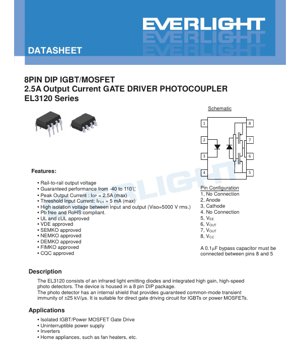
4.1 Pin Configuration and Function
The device is housed in a standard 8-pin DIP package. The pinout is as follows:
- Pin 1: No Connection (NC)
- Pin 2: Anode (A) of the input LED
- Pin 3: Cathode (K) of the input LED
- Pin 4: No Connection (NC)
- Pin 5: VEE (Negative supply/ground for output stage)
- Pin 6: VOUT (Gate drive output)
- Pin 7: VOUT (Gate drive output, connected internally to Pin 6)
- Pin 8: VCC (Positive supply for output stage)
The schematic diagram shows the internal connection: the photodetector drives a push-pull output stage connected between VCC and VEE. The datasheet explicitly states that a 0.1 µF bypass capacitor must be connected between pins 8 (VCC) and 5 (VEE) to ensure stable operation and minimize supply noise.
5. Soldering and Assembly Guidelines
The Absolute Maximum Ratings specify a soldering temperature (TSOL) of 260°C for 10 seconds. This is a typical value for lead-free (Pb-free) soldering processes. Designers should follow standard IPC guidelines for through-hole component soldering. The device should be stored within the specified storage temperature range of -55°C to +125°C in a dry environment to prevent moisture absorption, which could lead to popcorning during reflow (though primarily a concern for SMD parts).
6. Application Recommendations
6.1 Typical Application Circuits
The primary application is as an isolated gate driver for IGBTs and Power MOSFETs in circuits like motor drives, inverters, and UPS systems. A typical application circuit involves connecting the input pins (2 & 3) to a microcontroller or PWM controller via a current-limiting resistor. The output pins (6 & 7) connect directly to the gate of the power switch. An external gate resistor (RG) is almost always required in series with the gate to control switching speed, reduce ringing, and limit peak current. The value of RG is a trade-off between switching losses (faster is better) and electromagnetic interference (EMI) and voltage overshoot (slower is better).
6.2 Design Considerations
- Input Circuit: The LED drive current must be sufficient to overcome the maximum input threshold current (5 mA) with margin, typically 10-16 mA is used. A series resistor calculates as RIN = (VCONTROL - VF) / IF.
- Output Circuit: The power supply for the output stage (VCC to VEE) must be within 15-30V and well-regulated. The 0.1 µF bypass capacitor is mandatory and should be placed as close as possible to the device pins.
- Gate Drive: The peak output current of 2.5A is suitable for switches with moderate gate charge. For very large IGBTs, verify that the driver can deliver the required charge within the desired switching time. The pull-up and pull-down capabilities are symmetric, which is beneficial.
- Isolation: Maintain proper creepage and clearance distances on the PCB layout between the input and output sides according to the target isolation voltage and relevant safety standards.
- Thermal Management: While the package can dissipate 300 mW, calculate the actual power dissipation based on supply voltage, supply current, output current, duty cycle, and switching frequency to ensure the junction temperature remains within limits.
7. Technical Comparison and Differentiation
The EL3120 positions itself in the market with a specific set of features. Its 2.5A output current places it in the mid-range for gate driver photocouplers, suitable for a wide array of applications without the cost and complexity of higher-current discrete driver stages. The guaranteed 25 kV/µs CMTI is a robust figure, providing strong noise immunity in challenging environments like motor drives. The wide operating temperature range (-40°C to +110°C) exceeds that of many commercial-grade parts, offering reliability for industrial and outdoor applications. The rail-to-rail output voltage capability ensures efficient use of the gate drive supply voltage, maximizing the gate signal applied to the switch.
8. Frequently Asked Questions (Based on Technical Parameters)
Q: Can I use a single 15V supply for the output stage?
A: Yes, the supply voltage range is 15V to 30V. A 15V supply is the minimum and is perfectly acceptable, though it will result in a lower gate drive voltage for the power switch compared to using a higher voltage.
Q: What is the purpose of having two output pins (6 and 7)?
A: The two pins are internally connected. This design helps reduce parasitic inductance in the connection to the gate, allows for a more robust current path for the high peak currents, and provides layout flexibility.
Q: How do I ensure the device turns on reliably?
A: Drive the input LED with a current significantly above the maximum specified input threshold current (IFLH = 5 mA). Using 10-16 mA, as shown in the test conditions, provides a good safety margin across temperature and device variations.
Q: Is an external gate resistor necessary?
A: Almost always, yes. While the driver can connect directly, a gate resistor (typically between 1-100 Ω) is used to control the switching speed, dampen parasitic oscillations, and limit the peak current seen by both the driver IC and the power switch's gate.
9. Practical Application Example
Scenario: Driving a 600V IGBT in a 3-phase inverter for a motor drive. The microcontroller generates PWM signals at 5V logic level. A current-limiting resistor is calculated for ~12 mA LED current (e.g., (5V - 1.5V)/12mA ≈ 290Ω). The output side is powered by an isolated 20V DC-DC converter. Pins 6 and 7 are connected via a 10Ω gate resistor to the IGBT's gate. A 0.1 µF ceramic capacitor is placed directly across pins 8 and 5. The UVLO feature ensures the IGBT gate is held low if the 20V supply sags during startup or fault conditions, preventing partial turn-on and excessive power dissipation. The high CMTI ensures that the rapid voltage swings (dv/dt) on the IGBT's collector do not cause false triggering of the driver output through the isolation barrier.
10. Operating Principle
The EL3120 operates on the principle of optical coupling. An electrical signal applied to the input side causes the infrared LED to emit light. This light traverses an optically transparent isolation barrier (typically made of silicone or similar material). On the output side, a photodetector, which is a monolithic integrated circuit, receives this light and converts it back into an electrical signal. This IC includes a photosensitive element, amplification stages, and a powerful output buffer capable of sourcing and sinking high peak currents. The key advantage is that the signal and power are transmitted via light, providing galvanic isolation that blocks high voltages, ground loops, and noise.
11. Industry Trends
The market for gate driver isolators continues to evolve. Trends include integration of more features into the isolator IC, such as advanced protection functions (desaturation detection, soft turn-off, Miller clamp), higher levels of integration with other system functions, and support for higher switching frequencies demanded by wide-bandgap semiconductors (SiC and GaN). There is also a push towards higher reliability, longer operational lifetimes, and enhanced safety certifications for automotive (AEC-Q100) and functional safety (ISO 26262) applications. Package sizes are also trending towards smaller surface-mount types for higher power density designs, though through-hole packages like the DIP remain popular for their robustness and ease of prototyping.
LED Specification Terminology
Complete explanation of LED technical terms
Photoelectric Performance
| Term | Unit/Representation | Simple Explanation | Why Important |
|---|---|---|---|
| Luminous Efficacy | lm/W (lumens per watt) | Light output per watt of electricity, higher means more energy efficient. | Directly determines energy efficiency grade and electricity cost. |
| Luminous Flux | lm (lumens) | Total light emitted by source, commonly called "brightness". | Determines if the light is bright enough. |
| Viewing Angle | ° (degrees), e.g., 120° | Angle where light intensity drops to half, determines beam width. | Affects illumination range and uniformity. |
| CCT (Color Temperature) | K (Kelvin), e.g., 2700K/6500K | Warmth/coolness of light, lower values yellowish/warm, higher whitish/cool. | Determines lighting atmosphere and suitable scenarios. |
| CRI / Ra | Unitless, 0–100 | Ability to render object colors accurately, Ra≥80 is good. | Affects color authenticity, used in high-demand places like malls, museums. |
| SDCM | MacAdam ellipse steps, e.g., "5-step" | Color consistency metric, smaller steps mean more consistent color. | Ensures uniform color across same batch of LEDs. |
| Dominant Wavelength | nm (nanometers), e.g., 620nm (red) | Wavelength corresponding to color of colored LEDs. | Determines hue of red, yellow, green monochrome LEDs. |
| Spectral Distribution | Wavelength vs intensity curve | Shows intensity distribution across wavelengths. | Affects color rendering and quality. |
Electrical Parameters
| Term | Symbol | Simple Explanation | Design Considerations |
|---|---|---|---|
| Forward Voltage | Vf | Minimum voltage to turn on LED, like "starting threshold". | Driver voltage must be ≥Vf, voltages add up for series LEDs. |
| Forward Current | If | Current value for normal LED operation. | Usually constant current drive, current determines brightness & lifespan. |
| Max Pulse Current | Ifp | Peak current tolerable for short periods, used for dimming or flashing. | Pulse width & duty cycle must be strictly controlled to avoid damage. |
| Reverse Voltage | Vr | Max reverse voltage LED can withstand, beyond may cause breakdown. | Circuit must prevent reverse connection or voltage spikes. |
| Thermal Resistance | Rth (°C/W) | Resistance to heat transfer from chip to solder, lower is better. | High thermal resistance requires stronger heat dissipation. |
| ESD Immunity | V (HBM), e.g., 1000V | Ability to withstand electrostatic discharge, higher means less vulnerable. | Anti-static measures needed in production, especially for sensitive LEDs. |
Thermal Management & Reliability
| Term | Key Metric | Simple Explanation | Impact |
|---|---|---|---|
| Junction Temperature | Tj (°C) | Actual operating temperature inside LED chip. | Every 10°C reduction may double lifespan; too high causes light decay, color shift. |
| Lumen Depreciation | L70 / L80 (hours) | Time for brightness to drop to 70% or 80% of initial. | Directly defines LED "service life". |
| Lumen Maintenance | % (e.g., 70%) | Percentage of brightness retained after time. | Indicates brightness retention over long-term use. |
| Color Shift | Δu′v′ or MacAdam ellipse | Degree of color change during use. | Affects color consistency in lighting scenes. |
| Thermal Aging | Material degradation | Deterioration due to long-term high temperature. | May cause brightness drop, color change, or open-circuit failure. |
Packaging & Materials
| Term | Common Types | Simple Explanation | Features & Applications |
|---|---|---|---|
| Package Type | EMC, PPA, Ceramic | Housing material protecting chip, providing optical/thermal interface. | EMC: good heat resistance, low cost; Ceramic: better heat dissipation, longer life. |
| Chip Structure | Front, Flip Chip | Chip electrode arrangement. | Flip chip: better heat dissipation, higher efficacy, for high-power. |
| Phosphor Coating | YAG, Silicate, Nitride | Covers blue chip, converts some to yellow/red, mixes to white. | Different phosphors affect efficacy, CCT, and CRI. |
| Lens/Optics | Flat, Microlens, TIR | Optical structure on surface controlling light distribution. | Determines viewing angle and light distribution curve. |
Quality Control & Binning
| Term | Binning Content | Simple Explanation | Purpose |
|---|---|---|---|
| Luminous Flux Bin | Code e.g., 2G, 2H | Grouped by brightness, each group has min/max lumen values. | Ensures uniform brightness in same batch. |
| Voltage Bin | Code e.g., 6W, 6X | Grouped by forward voltage range. | Facilitates driver matching, improves system efficiency. |
| Color Bin | 5-step MacAdam ellipse | Grouped by color coordinates, ensuring tight range. | Guarantees color consistency, avoids uneven color within fixture. |
| CCT Bin | 2700K, 3000K etc. | Grouped by CCT, each has corresponding coordinate range. | Meets different scene CCT requirements. |
Testing & Certification
| Term | Standard/Test | Simple Explanation | Significance |
|---|---|---|---|
| LM-80 | Lumen maintenance test | Long-term lighting at constant temperature, recording brightness decay. | Used to estimate LED life (with TM-21). |
| TM-21 | Life estimation standard | Estimates life under actual conditions based on LM-80 data. | Provides scientific life prediction. |
| IESNA | Illuminating Engineering Society | Covers optical, electrical, thermal test methods. | Industry-recognized test basis. |
| RoHS / REACH | Environmental certification | Ensures no harmful substances (lead, mercury). | Market access requirement internationally. |
| ENERGY STAR / DLC | Energy efficiency certification | Energy efficiency and performance certification for lighting. | Used in government procurement, subsidy programs, enhances competitiveness. |