Table of Contents
- 1. Product Overview
- 1.1 Core Advantages and Target Market
- 2. In-Depth Technical Parameter Analysis
- 2.1 Absolute Maximum Ratings
- 2.2 Electro-Optical Characteristics
- 3. Performance Curve Analysis
- 4. Mechanical and Package Information
- 4.1 Pin Configuration and Schematic
- 4.2 Package Dimensions and Options
- 4.3 Polarity and Device Marking
- 5. Soldering and Assembly Guidelines
- 5.1 Reflow Soldering Profile
- 5.2 Precautions for Use
- 6. Packaging and Ordering Information
- 6.1 Model Numbering System
- 6.2 Packing Specifications
- 7. Application Notes and Design Considerations
- 7.1 Typical Application Circuits
- 7.2 Design Considerations
- 8. Technical Comparison and Selection Guide
- 9. Frequently Asked Questions (Based on Technical Parameters)
- 9.1 Can this SSR switch AC loads?
- 9.2 What is the purpose of the photovoltaic diode array in the output detector?
- 9.3 How do I interface the input with a 5V microcontroller?
- 9.4 Why is the turn-on time for the EL860A longer than for the EL840A?
- 10. Operational Principle
- 11. Practical Design Case Study
- 12. Technology Trends and Context
1. Product Overview
The EL840A and EL860A are general-purpose, dual-channel solid-state relays (SSRs) packaged in a compact 8-pin DIP format. These devices utilize an optical coupling mechanism, featuring an AlGaAs infrared LED on the input side that is optically isolated from a high-voltage output detector circuit on the output side. The output detector consists of a photovoltaic diode array driving MOSFET switches. This configuration provides the electrical functionality equivalent to two independent Form A (normally open) electromechanical relays, offering superior reliability, longer life, and faster switching compared to their mechanical counterparts.
1.1 Core Advantages and Target Market
The primary advantages of this SSR series stem from its solid-state design. Key benefits include the complete absence of moving parts, which eliminates contact bounce, arcing, and mechanical wear, leading to exceptionally long operational life and high reliability. The optical isolation between input and output provides a high isolation voltage of 5000 Vrms, enhancing system safety and noise immunity. The devices are designed to control low-level analog signals with high sensitivity and speed. Their compact 8-pin DIP footprint makes them suitable for high-density PCB layouts. The target applications include industrial automation, telecommunications equipment, computer peripherals, and high-speed inspection machinery where reliable, fast, and isolated switching of signals or low-power loads is required.
2. In-Depth Technical Parameter Analysis
The performance of the EL840A and EL860A is defined by a comprehensive set of electrical, optical, and thermal parameters. Understanding these specifications is crucial for proper circuit design and reliable operation.
2.1 Absolute Maximum Ratings
These ratings define the stress limits beyond which permanent damage to the device may occur. Operation under these conditions is not guaranteed.
- Input (LED Side): The maximum continuous forward current (IF) is 50 mA. A reverse voltage (VR) of up to 5V can be applied. A peak forward current (IFP) of 1A is allowed under pulsed conditions (100Hz, 0.1% duty cycle). The input power dissipation (Pin) must not exceed 75 mW.
- Output (MOSFET Side): A critical differentiation between the EL840A and EL860A is their output voltage and current ratings. The EL840A has a breakdown voltage (VL) of 400V and a continuous load current (IL) rating of 120 mA. The EL860A is rated for a higher breakdown voltage of 600V but a lower continuous current of 50 mA. Designers must select the model based on their specific voltage and current requirements. The pulse load current (ILPeak) is 300 mA for the EL840A and 150 mA for the EL860A for a 100ms duration. The output power dissipation (Pout) is limited to 800 mW.
- Isolation & Thermal: The isolation voltage (Viso) between input and output is 5000 Vrms (tested for 1 minute). The device can operate within an ambient temperature range of -40°C to +85°C and can be stored from -40°C to +125°C. The soldering temperature should not exceed 260°C for more than 10 seconds during reflow processes.
2.2 Electro-Optical Characteristics
These parameters, typically specified at 25°C, define the operational behavior of the SSR.
- Input Characteristics: The forward voltage (VF) of the input LED is typically 1.18V at a drive current of 10mA, with a maximum of 1.5V. The reverse leakage current (IR) is a maximum of 1 µA at 5V reverse bias.
- Output Characteristics: The off-state leakage current (Ileak) is exceptionally low, with a maximum of 1 µA when the input LED is off and the output is at its maximum rated voltage. The on-resistance (Rd(ON)) is a key parameter affecting voltage drop and power loss. The EL840A has a typical Rd(ON) of 20Ω (max 30Ω), while the EL860A has a typical of 40Ω (max 70Ω) when driven with 10mA input current at maximum load.
- Transfer Characteristics: This defines the relationship between input and output. The LED turn-on current (IF(on)) required to fully activate the output MOSFETs is a maximum of 5mA for both models (typical 3mA). The LED turn-off current (IF(off)) is a minimum of 0.4mA, below which the output is guaranteed to be off. This defines the input current hysteresis.
- Switching Speed: The turn-on time (Ton) is the delay from applying the input current to the output reaching 90% of its on-state value. For the EL840A, it is typically 0.4ms (max 3ms), and for the EL860A, typically 1.4ms (max 3ms). The turn-off time (Toff) is typically 0.05ms (max 0.5ms) for both models. These are relatively fast for an SSR, suitable for many signal switching applications.
- Isolation Parameters: The isolation resistance (RI-O) is a minimum of 5 x 10¹⁰ Ω at 500V DC. The isolation capacitance (CI-O) is a maximum of 1.5 pF, which is important for high-frequency noise coupling considerations.
3. Performance Curve Analysis
While specific graphical data is referenced in the datasheet (Typical Electro-Optical Characteristics Curves, Turn on/Turn off Time diagrams), the textual data allows for analysis of key trends. The relationship between forward current and forward voltage for the input LED will follow a standard diode exponential curve. The on-resistance is specified at a specific condition; it will have a positive temperature coefficient, meaning it will increase as the junction temperature of the output MOSFETs rises. The switching times are load-dependent; the specified times are for a resistive load (RL = 200Ω). Capacitive or inductive loads will affect these times, potentially requiring snubber networks for protection and timing stability.
4. Mechanical and Package Information
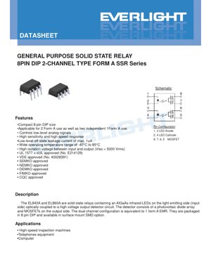
4.1 Pin Configuration and Schematic
The device uses a standard 8-pin DIP pinout. Pins 1 and 3 are the anodes for the two independent input LEDs. Pins 2 and 4 are the corresponding cathodes. The output side consists of two independent MOSFET switches. For each channel, the drain and source terminals are connected to pins 5, 6, 7, and 8 as per the internal schematic, allowing for flexible connection as a SPST switch.
4.2 Package Dimensions and Options
The product is offered in two primary package styles: a Standard DIP Type with through-hole leads, and an Option S1 Type which is a surface-mount leadform (low profile). Detailed dimensional drawings are provided for both, including body length, width, height, lead pitch (2.54mm standard for DIP), and lead dimensions. For the SMD option, a recommended pad layout is also supplied to ensure reliable soldering and mechanical strength.
4.3 Polarity and Device Marking
The device is marked on the top surface. The marking follows the format: "EL" (manufacturer identifier), followed by the part number (e.g., 860A), a one-digit year code (Y), a two-digit week code (WW), and an optional "V" denoting VDE-approved versions. Correct identification of pin 1, typically marked by a dot or notch on the package body, is essential for proper orientation.
5. Soldering and Assembly Guidelines
5.1 Reflow Soldering Profile
For surface-mount assemblies, a specific reflow temperature profile must be followed to prevent damage. The profile is compliant with IPC/JEDEC J-STD-020D. Key parameters include: a preheat stage from 150°C to 200°C over 60-120 seconds, a maximum ramp-up rate of 3°C/second, a time above liquidus (217°C) of 60-100 seconds, and a peak package body temperature of 260°C for a maximum of 30 seconds. These conditions ensure proper solder joint formation without exposing the internal semiconductor junctions to excessive thermal stress.
5.2 Precautions for Use
Several important design considerations are highlighted. The absolute maximum ratings for voltage, current, and power must never be exceeded. The output MOSFETs are not inherently protected against voltage transients or inductive kickback; external protection components like snubbers or TVS diodes may be necessary in harsh electrical environments. The low thermal mass of the package means attention must be paid to power dissipation and adequate PCB copper area for heat sinking, especially when operating near maximum load currents or at high ambient temperatures.
6. Packaging and Ordering Information
6.1 Model Numbering System
The part number follows the structure: EL8XXA(Y)(Z)-V.
- XX: Denotes the part number, either 40 (EL840A) or 60 (EL860A), defining the voltage/current rating.
- Y: Lead form option. "S1" denotes the surface-mount leadform. Omission indicates the standard through-hole DIP.
- Z: Tape and reel option for automated assembly (TA, TB, TU, TD). Omission indicates tube packaging.
- V: Suffix indicating VDE safety-approved option.
6.2 Packing Specifications
The standard DIP version is supplied in tubes holding 45 units. The surface-mount options (S1 with TA or TB tape) are supplied on reels of 1000 units each. Detailed tape dimensions are provided, including pocket size (A, B), pocket depth (D0, D1), feed hole pitch (P0), and reel width (W), which are critical for compatibility with automated pick-and-place equipment.
7. Application Notes and Design Considerations
7.1 Typical Application Circuits
The SSR can be used in two primary configurations: as two independent single-pole single-throw (SPST) switches or, by connecting the outputs appropriately, as a single Form A changeover or other configuration. The input LED is typically driven by a digital logic gate or a transistor, with a current-limiting resistor calculated based on the supply voltage and the desired LED current (e.g., 10-20 mA for full output activation). The output can switch DC or AC loads within its voltage and current ratings. For AC loads, the MOSFET body diodes will conduct during half-cycles, so the device is essentially a bidirectional switch.
7.2 Design Considerations
- Heat Management: Calculate power dissipation as Pdiss = IL2 * Rd(ON). Ensure the total device dissipation (PT = 850mW max) is not exceeded. Use sufficient PCB copper area as a heat sink.
- Load Compatibility: The SSR is ideal for resistive loads. For capacitive loads, inrush current may exceed ILPeak. For inductive loads, use a snubber network (RC across the load or a transient voltage suppressor) to clamp voltage spikes generated when switching off.
- Input Drive: Ensure the input current exceeds IF(on) for reliable turn-on and falls below IF(off) for reliable turn-off. Avoid slow input signal edges near the threshold currents.
- Isolation Integrity: Maintain proper creepage and clearance distances on the PCB between the input and output circuits to preserve the high isolation rating.
8. Technical Comparison and Selection Guide
The key differentiator within this series is the trade-off between voltage and current capability. The EL840A is optimized for applications requiring higher continuous current (up to 120mA) but at a lower voltage (400V). It features a lower on-resistance, leading to less voltage drop and power loss. The EL860A is designed for applications requiring a higher blocking voltage (600V) but with a lower continuous current (50mA). Its on-resistance is higher. Selection should be based on the peak voltage and steady-state current of the load. For loads with significant inrush current (like lamps or capacitors), the EL840A's higher pulse current rating (300mA vs. 150mA) may also be a deciding factor.
9. Frequently Asked Questions (Based on Technical Parameters)
9.1 Can this SSR switch AC loads?
Yes. The output MOSFET structure, with its inherent body diode, allows bidirectional current flow. Therefore, it can switch AC voltages within its breakdown voltage (VL) rating. The current rating applies to both DC and the peak value of AC.
9.2 What is the purpose of the photovoltaic diode array in the output detector?
The photovoltaic array generates a voltage when illuminated by the infrared LED from the input side. This voltage is used to drive the gates of the output MOSFETs, turning them on. This method provides the complete galvanic isolation, as no electrical connection is needed to bias the MOSFET gates.
9.3 How do I interface the input with a 5V microcontroller?
Use a simple series resistor. For example, with a microcontroller GPIO pin at 5V, an LED VF of ~1.2V, and a desired IF of 10mA, the resistor value R = (5V - 1.2V) / 0.01A = 380Ω. A standard 390Ω resistor would be suitable. Ensure the microcontroller can source the required current.
9.4 Why is the turn-on time for the EL860A longer than for the EL840A?
The longer typical turn-on time (1.4ms vs. 0.4ms) is likely related to the internal design of the higher-voltage MOSFETs in the EL860A, which may have different gate capacitance or the characteristics of the photovoltaic driver circuit optimized for the 600V process.
10. Operational Principle
The device operates on the principle of optical isolation and photovoltaic driving. When a forward current is applied to the input AlGaAs infrared LED, it emits light. This light crosses an isolation gap and strikes a photovoltaic diode array on the output side. The array converts the light energy into electrical energy, generating a voltage sufficient to bias the gates of the N-channel MOSFETs into conduction. This creates a low-resistance path between the drain and source terminals, closing the relay "contact." When the input current is removed, the light emission stops, the photovoltaic voltage decays, and the MOSFET gates discharge, turning the devices off and opening the circuit. The entire process involves no physical contact or magnetic coupling, ensuring long life and high noise immunity.
11. Practical Design Case Study
Scenario: Isolating a 24V DC, 80mA sensor signal from a data acquisition system's analog input.
Implementation: An EL840A is selected for its 120mA current rating (providing margin) and 400V voltage rating (far exceeding 24V). The sensor output drives the SSR input via a 330Ω resistor from a 5V rail, providing ~11mA to the LED, well above the 5mA maximum IF(on). The SSR output is connected between the 24V sensor signal and the data acquisition input. A 10kΩ pull-down resistor is placed on the acquisition input to define the logic low state when the SSR is off. The low leakage current (1µA max) ensures minimal error voltage across the pull-down resistor when the SSR is off. The fast switching speed (0.4ms typical) allows for rapid sampling if needed. The 5000Vrms isolation protects the sensitive acquisition circuitry from ground loops or transients in the sensor's environment.
12. Technology Trends and Context
Solid-state relays represent a mature but continuously evolving technology. The core trend is towards higher integration, smaller packages, and improved performance metrics. While this device uses a photovoltaic MOSFET driver, other technologies exist, such as those using phototriac drivers for AC switching or more advanced IC-based designs with integrated protection features (overcurrent, overtemperature). The move towards surface-mount packages (like the S1 option) aligns with the industry-wide trend for automated assembly and reduced board space. The high isolation voltage and multiple international safety approvals (UL, VDE, etc.) reflect the increasing importance of system safety and reliability in global markets, particularly in industrial and medical equipment. Future developments may focus on reducing on-resistance further, increasing switching speeds for high-frequency applications, and integrating more intelligent control and monitoring functions within the same isolated package.
LED Specification Terminology
Complete explanation of LED technical terms
Photoelectric Performance
| Term | Unit/Representation | Simple Explanation | Why Important |
|---|---|---|---|
| Luminous Efficacy | lm/W (lumens per watt) | Light output per watt of electricity, higher means more energy efficient. | Directly determines energy efficiency grade and electricity cost. |
| Luminous Flux | lm (lumens) | Total light emitted by source, commonly called "brightness". | Determines if the light is bright enough. |
| Viewing Angle | ° (degrees), e.g., 120° | Angle where light intensity drops to half, determines beam width. | Affects illumination range and uniformity. |
| CCT (Color Temperature) | K (Kelvin), e.g., 2700K/6500K | Warmth/coolness of light, lower values yellowish/warm, higher whitish/cool. | Determines lighting atmosphere and suitable scenarios. |
| CRI / Ra | Unitless, 0–100 | Ability to render object colors accurately, Ra≥80 is good. | Affects color authenticity, used in high-demand places like malls, museums. |
| SDCM | MacAdam ellipse steps, e.g., "5-step" | Color consistency metric, smaller steps mean more consistent color. | Ensures uniform color across same batch of LEDs. |
| Dominant Wavelength | nm (nanometers), e.g., 620nm (red) | Wavelength corresponding to color of colored LEDs. | Determines hue of red, yellow, green monochrome LEDs. |
| Spectral Distribution | Wavelength vs intensity curve | Shows intensity distribution across wavelengths. | Affects color rendering and quality. |
Electrical Parameters
| Term | Symbol | Simple Explanation | Design Considerations |
|---|---|---|---|
| Forward Voltage | Vf | Minimum voltage to turn on LED, like "starting threshold". | Driver voltage must be ≥Vf, voltages add up for series LEDs. |
| Forward Current | If | Current value for normal LED operation. | Usually constant current drive, current determines brightness & lifespan. |
| Max Pulse Current | Ifp | Peak current tolerable for short periods, used for dimming or flashing. | Pulse width & duty cycle must be strictly controlled to avoid damage. |
| Reverse Voltage | Vr | Max reverse voltage LED can withstand, beyond may cause breakdown. | Circuit must prevent reverse connection or voltage spikes. |
| Thermal Resistance | Rth (°C/W) | Resistance to heat transfer from chip to solder, lower is better. | High thermal resistance requires stronger heat dissipation. |
| ESD Immunity | V (HBM), e.g., 1000V | Ability to withstand electrostatic discharge, higher means less vulnerable. | Anti-static measures needed in production, especially for sensitive LEDs. |
Thermal Management & Reliability
| Term | Key Metric | Simple Explanation | Impact |
|---|---|---|---|
| Junction Temperature | Tj (°C) | Actual operating temperature inside LED chip. | Every 10°C reduction may double lifespan; too high causes light decay, color shift. |
| Lumen Depreciation | L70 / L80 (hours) | Time for brightness to drop to 70% or 80% of initial. | Directly defines LED "service life". |
| Lumen Maintenance | % (e.g., 70%) | Percentage of brightness retained after time. | Indicates brightness retention over long-term use. |
| Color Shift | Δu′v′ or MacAdam ellipse | Degree of color change during use. | Affects color consistency in lighting scenes. |
| Thermal Aging | Material degradation | Deterioration due to long-term high temperature. | May cause brightness drop, color change, or open-circuit failure. |
Packaging & Materials
| Term | Common Types | Simple Explanation | Features & Applications |
|---|---|---|---|
| Package Type | EMC, PPA, Ceramic | Housing material protecting chip, providing optical/thermal interface. | EMC: good heat resistance, low cost; Ceramic: better heat dissipation, longer life. |
| Chip Structure | Front, Flip Chip | Chip electrode arrangement. | Flip chip: better heat dissipation, higher efficacy, for high-power. |
| Phosphor Coating | YAG, Silicate, Nitride | Covers blue chip, converts some to yellow/red, mixes to white. | Different phosphors affect efficacy, CCT, and CRI. |
| Lens/Optics | Flat, Microlens, TIR | Optical structure on surface controlling light distribution. | Determines viewing angle and light distribution curve. |
Quality Control & Binning
| Term | Binning Content | Simple Explanation | Purpose |
|---|---|---|---|
| Luminous Flux Bin | Code e.g., 2G, 2H | Grouped by brightness, each group has min/max lumen values. | Ensures uniform brightness in same batch. |
| Voltage Bin | Code e.g., 6W, 6X | Grouped by forward voltage range. | Facilitates driver matching, improves system efficiency. |
| Color Bin | 5-step MacAdam ellipse | Grouped by color coordinates, ensuring tight range. | Guarantees color consistency, avoids uneven color within fixture. |
| CCT Bin | 2700K, 3000K etc. | Grouped by CCT, each has corresponding coordinate range. | Meets different scene CCT requirements. |
Testing & Certification
| Term | Standard/Test | Simple Explanation | Significance |
|---|---|---|---|
| LM-80 | Lumen maintenance test | Long-term lighting at constant temperature, recording brightness decay. | Used to estimate LED life (with TM-21). |
| TM-21 | Life estimation standard | Estimates life under actual conditions based on LM-80 data. | Provides scientific life prediction. |
| IESNA | Illuminating Engineering Society | Covers optical, electrical, thermal test methods. | Industry-recognized test basis. |
| RoHS / REACH | Environmental certification | Ensures no harmful substances (lead, mercury). | Market access requirement internationally. |
| ENERGY STAR / DLC | Energy efficiency certification | Energy efficiency and performance certification for lighting. | Used in government procurement, subsidy programs, enhances competitiveness. |