Table of Contents
- 1. Product Overview
- 2. Key Features and Advantages
- 3. Technical Specifications Deep Dive
- 3.1 Absolute Maximum Ratings
- 3.2 Electro-Optical Characteristics
- 4. Performance Curves and Graphical Data
- 5. Mechanical, Package, and Assembly Information
- 5.1 Pin Configuration and Schematic
- 5.2 Package Dimensions and Mounting
- 5.3 Device Marking
- 5.4 Soldering and Handling Guidelines
- 6. Packaging and Ordering Information
- 6.1 Model Numbering System
- 6.2 Packing Specifications
- 7. Application Guidelines and Design Considerations
- 7.1 Target Applications
- 7.2 Critical Design Considerations
- 8. Technical Comparison and Selection Guide
- 9. Frequently Asked Questions (FAQ)
- 9.1 Can this SSR switch AC loads?
- 9.2 What is the difference between Connection A, B, and C?
- 9.3 How do I calculate the power dissipation and heat generated?
- 9.4 Is a heat sink required?
- 10. Operational Principle
- 11. Industry Context and Trends
1. Product Overview
This document details a series of general-purpose solid state relays (SSRs) in a 6-pin DIP (Dual In-line Package) configuration. These devices are single-pole, single-throw (Form A) relays, meaning they provide a normally open (NO) contact. They are designed to replace traditional electromechanical relays (EMRs) in a wide range of applications, offering superior reliability, longer life, and silent operation due to the absence of moving parts.
The core technology involves an AlGaAs infrared LED on the input side, optically coupled to a high-voltage output detector circuit. This detector consists of a photovoltaic diode array and MOSFETs, enabling the control of both AC and DC loads. The optical isolation provides a high isolation voltage (5000 Vrms) between the low-voltage control circuit and the high-voltage load circuit, enhancing system safety and noise immunity.
2. Key Features and Advantages
- Normally Open (Form A) Configuration: Simple, single-channel switching.
- Low Operating Current: The input LED requires minimal drive current, making it compatible with low-power logic circuits and microcontrollers.
- Wide Output Voltage Range: Available in models with output withstand voltages from 60V to 600V (EL606A, EL625A, EL640A, EL660A), catering to various application voltage levels.
- Low On-Resistance: MOSFET-based output provides low conduction losses, improving efficiency and reducing heat generation.
- Wide Operating Temperature: Reliable operation from -40°C to +85°C, suitable for industrial and harsh environments.
- High Isolation Voltage: 5000 Vrms isolation between input and output ensures safety and protects sensitive control electronics.
- Industry Approvals: Certified to UL 1577, UL 508, VDE, SEMKO, NEMKO, DEMKO, FIMKO, and CQC standards, ensuring compliance with international safety and performance requirements.
- Package Options: Available in standard through-hole DIP and surface-mount (SMD) lead form variants.
3. Technical Specifications Deep Dive
3.1 Absolute Maximum Ratings
These are the stress limits beyond which permanent damage to the device may occur. Operation should always be within these limits.
- Input (LED Side): Maximum forward current (IF) is 50 mA, with a peak forward current (IFP) of 1 A under pulsed conditions. Reverse voltage (VR) is limited to 5 V.
- Output (Switch Side): Breakdown voltage (VL) defines the maximum voltage the output can block, ranging from 60V (EL606A) to 600V (EL660A). Continuous load current (IL) varies by model and connection type (A, B, C), from 50 mA to 800 mA. Pulse load current (ILPeak) is also specified for short-duration surges.
- Isolation: Withstands 5000 Vrms for 1 minute between input and output.
- Thermal: Operating temperature range is -40°C to +85°C. Storage temperature extends to 125°C. Maximum soldering temperature is 260°C for 10 seconds.
3.2 Electro-Optical Characteristics
These parameters define the operational performance of the SSR at 25°C.
- Input Characteristics: Typical forward voltage (VF) for the LED is 1.18V at 10mA. Reverse leakage current (IR) is very low (<1 µA).
- Output Characteristics - Off State: Leakage current (Ileak) when the SSR is off is specified as a maximum of 1 µA, indicating excellent blocking capability.
- Output Characteristics - On State: The key parameter is On-Resistance (Rd(ON)). This varies significantly between models and connection types:
- Connection A: Highest current rating, highest Rd(ON) (e.g., EL606A: 0.75Ω typ, 2.5Ω max).
- Connection B: Balanced rating, medium Rd(ON).
- Connection C: Lower current rating, lowest Rd(ON) (e.g., EL606A: 0.2Ω typ, 0.5Ω max).
- Output Capacitance (Cout): Ranges from 30 pF to 85 pF. Lower capacitance is beneficial for high-frequency switching to reduce losses.
- Transfer Characteristics: Defines the input current required to reliably turn the output on (IF(on), max 3 mA) and off (IF(off), min 0.4 mA). This ensures clear switching thresholds.
- Switching Speed: Turn-on time (Ton) is typically between 0.35 ms and 1.3 ms. Turn-off time (Toff) is very fast, typically 0.1 ms. These are slower than some SSRs but sufficient for many industrial control applications.
- Isolation Parameters: Isolation resistance (RI-O) is extremely high (>5×10¹⁰ Ω), and isolation capacitance (CI-O) is low (1.5 pF typ).
4. Performance Curves and Graphical Data
The datasheet includes typical characteristic curves (though not detailed in the provided text). These would typically illustrate:
- Forward Voltage vs. Forward Current (Vf-If): For the input LED, showing its diode-like behavior.
- On-Resistance vs. Load Current (Rd(ON)-IL): Showing how Rd(ON) may change with the amount of current being switched.
- On-Resistance vs. Ambient Temperature (Rd(ON)-Ta): Critical for thermal design, as Rd(ON) typically increases with temperature, leading to higher losses.
- Transfer Characteristics Graph: Plotting output status (on/off) versus input LED current, visually defining the turn-on/off thresholds and hysteresis.
These curves are essential for designers to understand device behavior under non-standard or varying conditions beyond the 25°C typical values.
5. Mechanical, Package, and Assembly Information
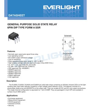
5.1 Pin Configuration and Schematic
The 6-pin DIP has a standard pinout:
- Pin 1: LED Anode (+)
- Pin 2: LED Cathode (-)
- Pin 4, 6: MOSFET Drain (Output terminals, typically interchangeable for DC)
- Pin 5: MOSFET Source (Common output terminal)
- Pin 3: Not connected (NC) internally, may be used for mechanical stability.
5.2 Package Dimensions and Mounting
Detailed mechanical drawings are provided for:
- Standard DIP Type: For through-hole PCB mounting.
- Option S1 Type (Low Profile Surface Mount): For SMD assembly.
- Recommended Pad Layout: For the SMD version, ensuring proper solder joint formation during reflow.
5.3 Device Marking
Devices are marked on the top with a code: "EL" prefix, part number (e.g., 660A), a 1-digit year code (Y), a 2-digit week code (WW), and a VDE option code (V). This allows for traceability.
5.4 Soldering and Handling Guidelines
Based on the Absolute Maximum Ratings:
- Reflow Soldering (SMD): Peak temperature must not exceed 260°C, and the time above 260°C should be limited to 10 seconds to prevent damage.
- Wave/Hand Soldering (DIP): Standard practices apply, but thermal stress should be minimized.
- ESD Precautions: Although MOSFET-based, the output is protected by the photovoltaic drive. Standard ESD handling for sensitive components is recommended.
- Storage: Store in dry, anti-static conditions within the -40°C to +125°C temperature range.
6. Packaging and Ordering Information
6.1 Model Numbering System
The part number follows the format: EL6XXA(Y)(Z)-V
- XX: Part number defining output voltage/current (06, 25, 40, 60).
- Y: Lead form option. 'S1' denotes surface mount low-profile. Blank denotes standard DIP.
- Z: Tape and reel option for SMD parts (TA, TB, TU, TD). Blank for tube packaging.
- V: Denotes VDE safety-approved option.
6.2 Packing Specifications
- Standard DIP: Packed in tubes, 65 units per tube.
- Surface Mount (S1): Packed on tape and reel, 1000 units per reel. Detailed tape dimensions (pocket size A, B, hole Do, D1, pitch E, F) and reel specifications are provided for automated pick-and-place machine setup.
7. Application Guidelines and Design Considerations
7.1 Target Applications
These SSRs are suited for a broad spectrum of applications requiring reliable, isolated switching:
- Telecommunication & Exchange Equipment: Signal routing, line card interfaces.
- Test & Measurement Equipment: Switching sensor inputs, multiplexing signals.
- Factory Automation (FA) & Office Automation (OA): Controlling solenoids, small motors, lamps, and heaters.
- Industrial Control Systems (ICS): PLC output modules, interface between logic and power circuits.
- Security Systems: Switching alarms, door locks, or camera power.
7.2 Critical Design Considerations
- Input Drive Circuit: Use a current-limiting resistor in series with the LED. Calculate resistor value based on supply voltage (e.g., 3.3V, 5V, 12V), desired LED current (5-10mA typical for guaranteed turn-on), and the LED's VF. Ensure the drive circuit can supply at least the maximum IF(on) (3mA) and can pull below IF(off) (0.4mA) to guarantee turn-off.
- Output Load Considerations:
- Voltage Rating: Select a model (EL606A/625A/640A/660A) where the maximum load voltage (including transients) is below the device's VL rating. Derating (e.g., using a 400V part for a 240VAC line) is good practice.
- Current Rating: Choose based on the continuous RMS or DC load current. Consider the connection type (A/B/C) trade-off. The load current must not exceed the specified IL for the chosen connection and model under worst-case temperature conditions.
- Inductive Loads: When switching inductive loads (relays, solenoids, motors), a snubber circuit (RC network) or a flyback diode (for DC) across the load is essential to suppress voltage spikes that can exceed the SSR's breakdown voltage.
- Inrush Current: For loads like lamps or capacitive loads with high turn-on surge, ensure the peak surge current is within the ILPeak rating. A negative temperature coefficient (NTC) thermistor or other inrush limiter may be needed.
- Thermal Management: Power dissipation (Pout) in the SSR is calculated as I_load² * Rds(on). At maximum current and elevated temperature, this can be significant. Ensure the PCB layout provides adequate copper area for heat sinking, especially for the SMD version. Do not exceed the maximum junction temperature, which is linked to the ambient temperature (Ta) and thermal resistance.
- PCB Layout: Maintain creepage and clearance distances on the PCB between input and output traces as per safety standards (e.g., IEC 61010-1). Keep high-current output traces short and wide.
8. Technical Comparison and Selection Guide
The four models in this series form a clear hierarchy based on voltage and current capability:
- EL606A (60V): For low-voltage DC applications. Offers the highest continuous current (up to 800mA in Connection C) and the lowest on-resistance.
- EL625A (250V): Suitable for 120VAC line voltage applications (with derating) or mid-range DC systems. Good balance of current (up to 300mA) and voltage.
- EL640A (400V): Ideal for 240VAC line voltage applications. Current rating up to 150mA.
- EL660A (600V): For high-voltage DC or demanding industrial AC lines with significant transients. Current rating up to 80mA.
Compared to Electromechanical Relays (EMRs): These SSRs offer no contact bounce, much longer life (billions of cycles), silent operation, and better resistance to shock and vibration. They are generally slower, have a higher initial cost, and have a non-zero on-resistance leading to heat dissipation.
Compared to other SSRs: The photovoltaic MOSFET coupling provides very low output leakage and stable on-resistance. It is different from triac-based SSRs used for AC switching, as these MOSFET-based relays can switch DC.
9. Frequently Asked Questions (FAQ)
9.1 Can this SSR switch AC loads?
Yes. The MOSFET output is bidirectional when off. However, the body diode of a single MOSFET makes it unidirectional when on. For true AC switching, two MOSFETs are often used back-to-back. The datasheet states "enable AC/DC and DC only output connections." The schematic and connection diagrams (A, B, C) show a single MOSFET. Therefore, for AC switching, external circuitry or a specific connection configuration (likely involving both drain pins 4 & 6) is implied to block current in both directions when on. The designer must consult the detailed connection diagrams to implement AC switching correctly.
9.2 What is the difference between Connection A, B, and C?
These are different internal or external wiring configurations of the photovoltaic array and MOSFET(s) that trade off maximum load current (IL) for lower on-resistance (Rd(ON)). Connection A prioritizes high current capability. Connection C prioritizes lowest possible conduction loss (lowest Rd(ON)). Connection B offers a middle ground. The choice depends on whether your design is limited by current handling or power dissipation/voltage drop.
9.3 How do I calculate the power dissipation and heat generated?
Power dissipated in the SSR (P_ssr) is almost entirely from the output MOSFET: P_ssr = I_load² * Rds(on). Use the maximum Rds(on) from the datasheet at your expected operating junction temperature for a conservative estimate. For example, an EL606A in Connection C (Rds(on)_max = 0.5Ω) switching 500mA DC dissipates P = (0.5)² * 0.5 = 0.125W. This heat must be conducted away via the pins and PCB copper to keep the junction temperature within limits.
9.4 Is a heat sink required?
For the SMD package at higher currents, yes. The need depends on the calculated power dissipation, the thermal resistance from junction-to-ambient (RθJA) for your PCB layout, and the maximum ambient temperature. If the calculated junction temperature (Tj = Ta + (P_ssr * RθJA)) approaches or exceeds 85°C, improved heat sinking (more copper, thermal vias, external heatsink) is necessary.
10. Operational Principle
The SSR operates on the principle of optical isolation and photovoltaic voltage generation. When a current flows through the input AlGaAs infrared LED, it emits light. This light is detected by a photovoltaic diode array on the output side. This array generates an open-circuit voltage sufficient to fully enhance the gate of the N-channel MOSFET(s) in the output stage. This turns the MOSFET on, creating a low-resistance path between its drain and source terminals, thus closing the "switch." When the LED current is removed, the photovoltaic voltage collapses, the MOSFET gate discharges, and the device turns off. The optical path provides the high electrical isolation.
11. Industry Context and Trends
Solid-state relays continue to gain market share over electromechanical relays in many applications due to demands for higher reliability, longer lifespan, and miniaturization. Trends driving SSR development include:
- Higher Power Density: Developing SSRs with lower Rds(on) to handle more current in smaller packages, reducing board space.
- Integration: Incorporating protection features like over-current detection, thermal shutdown, and state feedback into the SSR package.
- Wider Voltage Ranges: Devices for both low-voltage (e.g., 12V/24V automotive/industrial) and mains-voltage applications are in demand.
- Improved Isolation Materials: Enhancing safety ratings and reliability through advanced mold compounds and internal construction.
LED Specification Terminology
Complete explanation of LED technical terms
Photoelectric Performance
| Term | Unit/Representation | Simple Explanation | Why Important |
|---|---|---|---|
| Luminous Efficacy | lm/W (lumens per watt) | Light output per watt of electricity, higher means more energy efficient. | Directly determines energy efficiency grade and electricity cost. |
| Luminous Flux | lm (lumens) | Total light emitted by source, commonly called "brightness". | Determines if the light is bright enough. |
| Viewing Angle | ° (degrees), e.g., 120° | Angle where light intensity drops to half, determines beam width. | Affects illumination range and uniformity. |
| CCT (Color Temperature) | K (Kelvin), e.g., 2700K/6500K | Warmth/coolness of light, lower values yellowish/warm, higher whitish/cool. | Determines lighting atmosphere and suitable scenarios. |
| CRI / Ra | Unitless, 0–100 | Ability to render object colors accurately, Ra≥80 is good. | Affects color authenticity, used in high-demand places like malls, museums. |
| SDCM | MacAdam ellipse steps, e.g., "5-step" | Color consistency metric, smaller steps mean more consistent color. | Ensures uniform color across same batch of LEDs. |
| Dominant Wavelength | nm (nanometers), e.g., 620nm (red) | Wavelength corresponding to color of colored LEDs. | Determines hue of red, yellow, green monochrome LEDs. |
| Spectral Distribution | Wavelength vs intensity curve | Shows intensity distribution across wavelengths. | Affects color rendering and quality. |
Electrical Parameters
| Term | Symbol | Simple Explanation | Design Considerations |
|---|---|---|---|
| Forward Voltage | Vf | Minimum voltage to turn on LED, like "starting threshold". | Driver voltage must be ≥Vf, voltages add up for series LEDs. |
| Forward Current | If | Current value for normal LED operation. | Usually constant current drive, current determines brightness & lifespan. |
| Max Pulse Current | Ifp | Peak current tolerable for short periods, used for dimming or flashing. | Pulse width & duty cycle must be strictly controlled to avoid damage. |
| Reverse Voltage | Vr | Max reverse voltage LED can withstand, beyond may cause breakdown. | Circuit must prevent reverse connection or voltage spikes. |
| Thermal Resistance | Rth (°C/W) | Resistance to heat transfer from chip to solder, lower is better. | High thermal resistance requires stronger heat dissipation. |
| ESD Immunity | V (HBM), e.g., 1000V | Ability to withstand electrostatic discharge, higher means less vulnerable. | Anti-static measures needed in production, especially for sensitive LEDs. |
Thermal Management & Reliability
| Term | Key Metric | Simple Explanation | Impact |
|---|---|---|---|
| Junction Temperature | Tj (°C) | Actual operating temperature inside LED chip. | Every 10°C reduction may double lifespan; too high causes light decay, color shift. |
| Lumen Depreciation | L70 / L80 (hours) | Time for brightness to drop to 70% or 80% of initial. | Directly defines LED "service life". |
| Lumen Maintenance | % (e.g., 70%) | Percentage of brightness retained after time. | Indicates brightness retention over long-term use. |
| Color Shift | Δu′v′ or MacAdam ellipse | Degree of color change during use. | Affects color consistency in lighting scenes. |
| Thermal Aging | Material degradation | Deterioration due to long-term high temperature. | May cause brightness drop, color change, or open-circuit failure. |
Packaging & Materials
| Term | Common Types | Simple Explanation | Features & Applications |
|---|---|---|---|
| Package Type | EMC, PPA, Ceramic | Housing material protecting chip, providing optical/thermal interface. | EMC: good heat resistance, low cost; Ceramic: better heat dissipation, longer life. |
| Chip Structure | Front, Flip Chip | Chip electrode arrangement. | Flip chip: better heat dissipation, higher efficacy, for high-power. |
| Phosphor Coating | YAG, Silicate, Nitride | Covers blue chip, converts some to yellow/red, mixes to white. | Different phosphors affect efficacy, CCT, and CRI. |
| Lens/Optics | Flat, Microlens, TIR | Optical structure on surface controlling light distribution. | Determines viewing angle and light distribution curve. |
Quality Control & Binning
| Term | Binning Content | Simple Explanation | Purpose |
|---|---|---|---|
| Luminous Flux Bin | Code e.g., 2G, 2H | Grouped by brightness, each group has min/max lumen values. | Ensures uniform brightness in same batch. |
| Voltage Bin | Code e.g., 6W, 6X | Grouped by forward voltage range. | Facilitates driver matching, improves system efficiency. |
| Color Bin | 5-step MacAdam ellipse | Grouped by color coordinates, ensuring tight range. | Guarantees color consistency, avoids uneven color within fixture. |
| CCT Bin | 2700K, 3000K etc. | Grouped by CCT, each has corresponding coordinate range. | Meets different scene CCT requirements. |
Testing & Certification
| Term | Standard/Test | Simple Explanation | Significance |
|---|---|---|---|
| LM-80 | Lumen maintenance test | Long-term lighting at constant temperature, recording brightness decay. | Used to estimate LED life (with TM-21). |
| TM-21 | Life estimation standard | Estimates life under actual conditions based on LM-80 data. | Provides scientific life prediction. |
| IESNA | Illuminating Engineering Society | Covers optical, electrical, thermal test methods. | Industry-recognized test basis. |
| RoHS / REACH | Environmental certification | Ensures no harmful substances (lead, mercury). | Market access requirement internationally. |
| ENERGY STAR / DLC | Energy efficiency certification | Energy efficiency and performance certification for lighting. | Used in government procurement, subsidy programs, enhances competitiveness. |