Table of Contents
- 1. Product Overview
- 2. Technical Specifications Deep Dive
- 2.1 Absolute Maximum Ratings
- 2.2 Electro-Optical Characteristics
- 2.3 Reliability and Handling
- 3. Binning System Explanation
- 3.1 Forward Voltage Binning
- 3.2 Luminous Flux Binning
- 3.3 Color (White) Binning
- 4. Performance Curve Analysis
- 4.1 Forward Voltage vs. Forward Current (VF-IF Curve)
- 4.2 Luminous Flux vs. Forward Current
- 4.3 Correlated Color Temperature (CCT) vs. Forward Current
- 4.4 Forward Current Derating Curve
- 4.5 Relative Spectral Distribution & Radiation Pattern
- 5. Mechanical & Package Information
- 5.1 Package Dimensions
- 5.2 Polarity Identification
- 6. Soldering & Assembly Guidelines
- 7. Packaging & Ordering Information
- 7.1 Tape and Reel Packaging
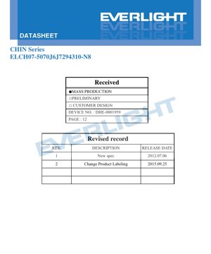
- 7.2 Label Explanation
- 8. Application Suggestions
- 8.1 Typical Application Scenarios
- 8.2 Design Considerations
- 9. Technical Comparison & Differentiation
- 10. Frequently Asked Questions (Based on Technical Parameters)
- 10.1 Can I drive this LED at 1000mA continuously?
- 10.2 What is the difference between the J6 and J7 flux bin?
- 10.3 How do I interpret the voltage bin code "2932"?
- 10.4 Is a heatsink absolutely necessary?
- 11. Design-in Case Study
- 12. Technical Principle Introduction
- 13. Industry Trends & Context
1. Product Overview
The ELCH07-5070J6J7294310-N8 is a high-power white LED component designed for applications requiring high luminous output and reliability. It belongs to the CHIN series and is characterized by its compact surface-mount package. The device is specified for mass production, indicating its maturity and stability for volume manufacturing.
The core technology is based on InGaN (Indium Gallium Nitride) semiconductor materials, which are engineered to emit white light. This LED is not designed for reverse bias operation, a critical consideration for circuit designers.
2. Technical Specifications Deep Dive
This section provides a detailed, objective analysis of the key technical parameters specified in the datasheet.
2.1 Absolute Maximum Ratings
The absolute maximum ratings define the limits beyond which permanent damage to the device may occur. Operating continuously at or near these limits is strongly discouraged.
- DC Forward Current (IF): 350 mA. This is the maximum continuous forward current the LED can handle.
- Peak Pulse Current (IPulse): 1500 mA. This high current is permissible only under specific pulsed conditions: a maximum pulse width of 400ms and a maximum duty cycle of 10% (e.g., 400ms ON, 3600ms OFF). This mode is typical for camera flash applications.
- ESD Resistance (VB): 8000 V (Human Body Model). This high rating indicates robust electrostatic discharge protection, which is crucial for handling during assembly and in the final application.
- Junction Temperature (TJ): 125 °C. The maximum allowable temperature of the semiconductor junction itself.
- Thermal Resistance (Rθ): 10 °C/W (junction to lead). This parameter is vital for thermal management design. It indicates that for every watt of power dissipated, the junction temperature will rise 10°C above the lead (solder pad) temperature. Effective heat sinking is required to maintain TJ within limits.
- Operating & Storage Temperature: -40°C to +85°C / -40°C to +110°C, respectively.
- Power Dissipation (Pulse Mode): 6 W. This is the maximum power the package can handle in pulsed operation, related to the peak pulse current rating.
- Soldering Temperature: 260°C maximum, with a limit of 2 reflow cycles.
- Viewing Angle (2θ1/2): 125 degrees (±5°). This wide viewing angle is characteristic of a Lambertian or near-Lambertian emission pattern.
2.2 Electro-Optical Characteristics
These parameters are tested under standard conditions (Tsolder pad = 25°C, 50ms pulse) and represent typical performance.
- Luminous Flux (Φv): 200-300 lm, with a typical value of 240 lm at IF = 1000mA. A measurement tolerance of ±10% applies. This high output makes it suitable for illumination tasks.
- Forward Voltage (VF): 2.95V to 4.35V at IF = 1000mA, with a measurement tolerance of ±0.1V. The wide range necessitates careful driver design and is managed through binning.
- Correlated Color Temperature (CCT): 5000K to 7000K. The typical value is 6000K, placing it in the "cool white" range.
- Optical Efficiency: 65 lm/W at 1000mA. This is a key figure of merit for energy efficiency.
2.3 Reliability and Handling
- Moisture Sensitivity Level (MSL): Class 1. This is the most robust level, meaning the device has an unlimited floor life at ≤30°C/85% RH and does not require baking before reflow soldering under standard conditions.
- Reliability Test: All specifications are assured by a 1000-hour reliability test, with the criterion that the luminous flux degradation is less than 30%.
- Test Condition Note: All reliability and correlation data are tested under "superior thermal management" using a 1.0 x 1.0 cm² Metal Core Printed Circuit Board (MCPCB). Real-world performance may vary if thermal management is less effective.
3. Binning System Explanation
To ensure consistency in mass production, LEDs are sorted (binned) based on key parameters. The part number ELCH07-5070J6J7294310-N8 encodes some of these bins.
3.1 Forward Voltage Binning
The forward voltage is binned into five codes (2932, 3235, 3538, 3841, 4143). The code indicates the min and max voltage in tenths of a volt. For example, bin "2932" covers VF from 2.95V to 3.25V. The "2932" in the part number indicates this specific LED falls into this voltage bin.
3.2 Luminous Flux Binning
The luminous flux is binned into two primary codes at 1000mA: J6 (200-250 lm) and J7 (250-300 lm). The "J6" in the part number specifies the luminous flux bin.
3.3 Color (White) Binning
The white color point is defined on the CIE 1931 chromaticity diagram and correlated to a Color Temperature (CCT) range. Two primary bins are defined:
- Bin 5057: CCT range 5000K to 5700K. Defined by a quadrilateral on the CIE chart.
- Bin 5770: CCT range 5700K to 7000K. Defined by a different quadrilateral.
4. Performance Curve Analysis
The datasheet provides several graphs illustrating performance trends. Understanding these is key for design optimization.
4.1 Forward Voltage vs. Forward Current (VF-IF Curve)
The curve shows a non-linear relationship. VF increases with IF, starting around 2.4V at very low current and reaching approximately 4.0V at 1500mA. This curve is essential for selecting an appropriate constant-current driver and calculating power dissipation (Pd = VF * IF).
4.2 Luminous Flux vs. Forward Current
The relative luminous flux increases sub-linearly with current. While output rises with current, the efficiency (lm/W) typically decreases at higher currents due to increased heat and "droop" effects in the semiconductor. The curve shows the relative output, with 1000mA as the reference point (1.0 on the Y-axis).
4.3 Correlated Color Temperature (CCT) vs. Forward Current
The CCT shows a slight variation with drive current, increasing from around 5600K at low current to about 6000K at 1000mA. This shift is important for applications where consistent color is critical.
4.4 Forward Current Derating Curve
This is arguably the most critical graph for reliable operation. It shows the maximum allowable continuous forward current as a function of the solder pad temperature (Tsolder pad). The curve is based on maintaining the junction temperature (TJ) at or below its maximum of 125°C. For example:
- At Tsolder pad = 25°C, the max current is ~600mA.
- At Tsolder pad = 75°C, the max current drops to ~300mA.
- At Tsolder pad = 100°C, the max current is nearly 0mA.
4.5 Relative Spectral Distribution & Radiation Pattern
The spectral graph shows a broad emission peak in the blue region (around 450nm) from the InGaN chip, combined with a broader yellow phosphor emission, resulting in white light. The radiation pattern graphs confirm a Lambertian distribution (cosine law), with equal intensity patterns on the X and Y axes, providing a wide, uniform viewing angle of 125 degrees.
5. Mechanical & Package Information
5.1 Package Dimensions
The LED is in a surface-mount package with a footprint of approximately 7.0mm x 7.0mm (as indicated by "5070" in the part number, likely 5.0mm x 7.0mm or 7.0mm x 7.0mm). The exact dimensional drawing shows key features including the solder pads, lens shape, and polarity indicator. Tolerances are typically ±0.1mm unless otherwise specified. The package includes an integrated lens that shapes the 125-degree viewing angle.
5.2 Polarity Identification
The package includes markings or physical features (like a chamfered corner) to identify the anode and cathode. Correct polarity is essential during assembly to prevent damage from reverse connection.
6. Soldering & Assembly Guidelines
- Reflow Soldering: The maximum soldering temperature is 260°C. The component can withstand a maximum of 2 reflow cycles. Standard lead-free reflow profiles (IPC/JEDEC J-STD-020) are applicable.
- Thermal Management: This is the paramount concern. The low thermal resistance (10°C/W) is only effective if the solder pads are connected to a sufficiently sized thermal pad on the PCB, which in turn must be connected to a heat sink. The use of an MCPCB or insulated metal substrate (IMS) is highly recommended for any application driving the LED near its maximum ratings.
- ESD Precautions: Although rated for 8kV HBM, standard ESD handling procedures (grounded workstations, wrist straps) should still be followed.
- Storage: As an MSL Level 1 device, no special dry storage is required under normal factory conditions.
7. Packaging & Ordering Information
7.1 Tape and Reel Packaging
The LEDs are supplied in moisture-resistant packing on embossed carrier tapes. Each reel contains 2000 pieces. The carrier tape has dimensions to ensure secure holding and proper orientation (polarity) during automated pick-and-place assembly. Reel dimensions are provided for integration into automated assembly equipment.
7.2 Label Explanation
The packaging label includes several key fields:
- P/N: The full part number (e.g., ELCH07-5070J6J7294310-N8).
- LOT NO: Traceability code for manufacturing batch.
- QTY: Quantity in the package.
- CAT (Luminous Flux Bin): e.g., J6.
- HUE (Color Bin): e.g., 72943.
- REF (Forward Voltage Bin): e.g., 2932.
- MSL-X: Moisture Sensitivity Level.
8. Application Suggestions
8.1 Typical Application Scenarios
The datasheet lists several applications, which can be prioritized based on the LED's characteristics:
- Mobile Phone Camera Flash / Strobe Light: The high peak pulse current (1500mA) and high luminous flux make this a primary application. The brief, high-power pulses are ideal for illuminating scenes for photography.
- Torch Light for DV / Portable Lighting: The high continuous output (when properly heatsunk) suits handheld video lights or flashlights.
- Specialized Indoor/Outdoor Lighting: Including orientation marker lights (exit signs, step lights), decorative lighting, and automotive interior/exterior illumination. The wide viewing angle is beneficial for area lighting.
- TFT Backlighting: For larger displays requiring high brightness, though secondary optics would be needed to direct the light.
8.2 Design Considerations
- Driver Selection: A constant-current driver is mandatory. The driver must be capable of supplying up to the required current (considering derating) and withstand the maximum VF of the selected bin. For flash applications, a driver capable of delivering high-current pulses is needed.
- Thermal Design: This cannot be overstated. Calculate the expected power dissipation (VF * IF). Use the thermal resistance (Rθ) and the derating curve to determine the necessary heat sinking to keep the solder pad temperature low enough to allow the desired drive current. Finite Element Analysis (FEA) thermal simulation is recommended for critical designs.
- Optical Design: The Lambertian pattern provides wide coverage. For focused beams (e.g., a flashlight), a secondary reflector or collimating lens will be required.
- Binning Consistency: For applications where multiple LEDs are used together (e.g., in an array for a video light), specify tight bins for forward voltage, flux, and especially color to ensure uniform appearance and balanced current sharing.
9. Technical Comparison & Differentiation
While a direct competitor comparison isn't in the datasheet, key differentiating features of this LED can be inferred:
- High Pulse Current Capability: The 1500mA pulse rating is a standout feature tailored for camera flash applications, which many general-purpose high-power LEDs do not emphasize.
- Robust ESD Protection: 8kV HBM is a high level of protection, improving reliability in end-user handling and assembly.
- MSL Level 1: Simplifies inventory management and assembly process compared to LEDs with higher MSL ratings (3, 2a, etc.) that require dry packing and baking.
- Explicit Reliability Data: The mention of a 1000-hour test with a <30% flux degradation criterion provides a quantitative reliability claim.
- Comprehensive Binning: The detailed binning structure for voltage, flux, and color allows designers to select the precise performance grade needed for their application, enabling higher quality and consistency in the final product.
10. Frequently Asked Questions (Based on Technical Parameters)
10.1 Can I drive this LED at 1000mA continuously?
Answer: Not without exceptional thermal management. The 1000mA rating is given under specific test conditions (50ms pulse, Tsolder pad=25°C). The derating curve shows that for continuous operation (DC), the maximum current is significantly lower—around 600mA at a 25°C solder pad temperature, and lower at higher temperatures. Continuous operation at 1000mA would almost certainly exceed the maximum junction temperature, leading to rapid degradation and failure.
10.2 What is the difference between the J6 and J7 flux bin?
Answer: The J6 bin covers luminous flux from 200 to 250 lumens at 1000mA, while the J7 bin covers 250 to 300 lumens. The "J6" in the part number specifies the minimum guaranteed flux for this particular device is in the lower range. For applications requiring maximum brightness, specifying the J7 bin is necessary.
10.3 How do I interpret the voltage bin code "2932"?
Answer: The code "2932" means the forward voltage of LEDs in this bin falls between 2.95 volts ("29" representing 2.9, with the last digit specifying the hundredths) and 3.25 volts ("32"). This allows designers to predict the power consumption and required driver voltage headroom more accurately.
10.4 Is a heatsink absolutely necessary?
Answer: Yes, for any operation beyond very low currents. The thermal resistance of 10°C/W means that even at a modest 350mA and a VF of 3.5V (dissipating about 1.23W), the junction temperature would be 12.3°C above the solder pad temperature. Without a heatsink, the solder pad temperature will quickly rise towards the ambient temperature plus this delta, pushing the junction temperature towards its limit. Proper thermal design is non-negotiable for performance and longevity.
11. Design-in Case Study
Scenario: Designing a smartphone camera flash module.
- Requirement: Need a very bright, short-duration flash. Assume a pulse width of 300ms, with a duty cycle < 10%.
- LED Selection: This LED is suitable due to its 1500mA peak pulse rating and high luminous output.
- Drive Condition: Decide to drive it at 1200mA during the pulse. Check the VF-IF curve: VF ~ 4.1V. Pulse power = 4.92W.
- Thermal Check: The pulse is short (300ms), so the average power is low due to the low duty cycle. The primary thermal concern is the heat accumulated during a burst of photos. The small size of a phone limits heatsinking. The design must ensure the solder pad temperature does not exceed, for example, 80°C during a photo session, referring to the derating curve.
- Driver: Select a compact, Li-ion battery compatible flash LED driver IC that can deliver 1200mA pulses and has safety timers.
- Optics: Use a simple diffuser or reflector to spread the light and avoid hotspots in photos.
- Binning: Specify a tight color bin (e.g., 5770) and a single voltage bin (e.g., 3538) to ensure consistent flash color and driver performance across all manufactured phones.
12. Technical Principle Introduction
This LED generates white light using a common and efficient method: Phosphor-Converted White Light.
- A semiconductor chip made of InGaN emits high-energy blue light when electrical current passes through it (electroluminescence).
- This blue light is partially absorbed by a layer of yellow (or yellow and red) phosphor material that is deposited directly on or near the chip.
- The phosphor re-emits the absorbed energy as lower-energy yellow (and red) light through a process called photoluminescence.
- The remaining unabsorbed blue light mixes with the emitted yellow/red light, and the human eye perceives this mixture as white light. The exact proportions determine the Correlated Color Temperature (CCT)—more blue results in "cool white" (higher CCT, like 6000K), while more yellow/red results in "warm white" (lower CCT).
13. Industry Trends & Context
This datasheet reflects several ongoing trends in the high-power LED industry:
- Increased Integration for Specific Applications: Rather than being a generic component, this LED is clearly optimized for camera flash and portable lighting, with specs like high pulse current taking precedence over extreme continuous drive ratings. This shows a move towards application-specific optimization.
- Emphasis on Reliability and Quantification: The inclusion of explicit reliability test criteria (1000hr, <30% degradation) and detailed thermal derating data responds to market demand for predictable longevity, especially in consumer electronics where warranty costs are a concern.
- Advanced Binning for Quality: The multi-parameter binning (flux, voltage, color) allows for higher quality and consistency in end products. This is crucial for applications like display backlighting or architectural lighting where color uniformity is visible and important.
- Robustness for Automated Assembly: Features like MSL Level 1, tape-and-reel packaging, and clear polarity marking are designed for compatibility with high-speed, automated Surface-Mount Technology (SMT) assembly lines, reducing manufacturing cost and defect rates.
- Thermal Management as a First-Order Design Constraint: The prominence of thermal data (Rθ, derating curves) underscores that the performance of modern high-power LEDs is fundamentally limited by heat dissipation, not just electrical or optical properties. Successful designs treat the LED and its heatsink as a single integrated system.
LED Specification Terminology
Complete explanation of LED technical terms
Photoelectric Performance
| Term | Unit/Representation | Simple Explanation | Why Important |
|---|---|---|---|
| Luminous Efficacy | lm/W (lumens per watt) | Light output per watt of electricity, higher means more energy efficient. | Directly determines energy efficiency grade and electricity cost. |
| Luminous Flux | lm (lumens) | Total light emitted by source, commonly called "brightness". | Determines if the light is bright enough. |
| Viewing Angle | ° (degrees), e.g., 120° | Angle where light intensity drops to half, determines beam width. | Affects illumination range and uniformity. |
| CCT (Color Temperature) | K (Kelvin), e.g., 2700K/6500K | Warmth/coolness of light, lower values yellowish/warm, higher whitish/cool. | Determines lighting atmosphere and suitable scenarios. |
| CRI / Ra | Unitless, 0–100 | Ability to render object colors accurately, Ra≥80 is good. | Affects color authenticity, used in high-demand places like malls, museums. |
| SDCM | MacAdam ellipse steps, e.g., "5-step" | Color consistency metric, smaller steps mean more consistent color. | Ensures uniform color across same batch of LEDs. |
| Dominant Wavelength | nm (nanometers), e.g., 620nm (red) | Wavelength corresponding to color of colored LEDs. | Determines hue of red, yellow, green monochrome LEDs. |
| Spectral Distribution | Wavelength vs intensity curve | Shows intensity distribution across wavelengths. | Affects color rendering and quality. |
Electrical Parameters
| Term | Symbol | Simple Explanation | Design Considerations |
|---|---|---|---|
| Forward Voltage | Vf | Minimum voltage to turn on LED, like "starting threshold". | Driver voltage must be ≥Vf, voltages add up for series LEDs. |
| Forward Current | If | Current value for normal LED operation. | Usually constant current drive, current determines brightness & lifespan. |
| Max Pulse Current | Ifp | Peak current tolerable for short periods, used for dimming or flashing. | Pulse width & duty cycle must be strictly controlled to avoid damage. |
| Reverse Voltage | Vr | Max reverse voltage LED can withstand, beyond may cause breakdown. | Circuit must prevent reverse connection or voltage spikes. |
| Thermal Resistance | Rth (°C/W) | Resistance to heat transfer from chip to solder, lower is better. | High thermal resistance requires stronger heat dissipation. |
| ESD Immunity | V (HBM), e.g., 1000V | Ability to withstand electrostatic discharge, higher means less vulnerable. | Anti-static measures needed in production, especially for sensitive LEDs. |
Thermal Management & Reliability
| Term | Key Metric | Simple Explanation | Impact |
|---|---|---|---|
| Junction Temperature | Tj (°C) | Actual operating temperature inside LED chip. | Every 10°C reduction may double lifespan; too high causes light decay, color shift. |
| Lumen Depreciation | L70 / L80 (hours) | Time for brightness to drop to 70% or 80% of initial. | Directly defines LED "service life". |
| Lumen Maintenance | % (e.g., 70%) | Percentage of brightness retained after time. | Indicates brightness retention over long-term use. |
| Color Shift | Δu′v′ or MacAdam ellipse | Degree of color change during use. | Affects color consistency in lighting scenes. |
| Thermal Aging | Material degradation | Deterioration due to long-term high temperature. | May cause brightness drop, color change, or open-circuit failure. |
Packaging & Materials
| Term | Common Types | Simple Explanation | Features & Applications |
|---|---|---|---|
| Package Type | EMC, PPA, Ceramic | Housing material protecting chip, providing optical/thermal interface. | EMC: good heat resistance, low cost; Ceramic: better heat dissipation, longer life. |
| Chip Structure | Front, Flip Chip | Chip electrode arrangement. | Flip chip: better heat dissipation, higher efficacy, for high-power. |
| Phosphor Coating | YAG, Silicate, Nitride | Covers blue chip, converts some to yellow/red, mixes to white. | Different phosphors affect efficacy, CCT, and CRI. |
| Lens/Optics | Flat, Microlens, TIR | Optical structure on surface controlling light distribution. | Determines viewing angle and light distribution curve. |
Quality Control & Binning
| Term | Binning Content | Simple Explanation | Purpose |
|---|---|---|---|
| Luminous Flux Bin | Code e.g., 2G, 2H | Grouped by brightness, each group has min/max lumen values. | Ensures uniform brightness in same batch. |
| Voltage Bin | Code e.g., 6W, 6X | Grouped by forward voltage range. | Facilitates driver matching, improves system efficiency. |
| Color Bin | 5-step MacAdam ellipse | Grouped by color coordinates, ensuring tight range. | Guarantees color consistency, avoids uneven color within fixture. |
| CCT Bin | 2700K, 3000K etc. | Grouped by CCT, each has corresponding coordinate range. | Meets different scene CCT requirements. |
Testing & Certification
| Term | Standard/Test | Simple Explanation | Significance |
|---|---|---|---|
| LM-80 | Lumen maintenance test | Long-term lighting at constant temperature, recording brightness decay. | Used to estimate LED life (with TM-21). |
| TM-21 | Life estimation standard | Estimates life under actual conditions based on LM-80 data. | Provides scientific life prediction. |
| IESNA | Illuminating Engineering Society | Covers optical, electrical, thermal test methods. | Industry-recognized test basis. |
| RoHS / REACH | Environmental certification | Ensures no harmful substances (lead, mercury). | Market access requirement internationally. |
| ENERGY STAR / DLC | Energy efficiency certification | Energy efficiency and performance certification for lighting. | Used in government procurement, subsidy programs, enhances competitiveness. |