Table of Contents
- 1. Product Overview
- 2. In-Depth Technical Parameter Analysis
- 2.1 Absolute Maximum Ratings
- 2.2 Electrical & Transfer Characteristics
- 2.3 Switching Characteristics
- 3. Mechanical & Package Information
- 3.1 Pin Configuration and Function
- 4. Truth Table and Functional Description
- 5. Application Guidelines and Design Considerations
- 5.1 Typical Application Circuits
- 5.2 Design Considerations
- 6. Compliance and Reliability Information
- 7. Test Circuits and Waveform Definitions
- 8. Soldering and Handling
- 9. Technical Comparison and Positioning
- 10. Frequently Asked Questions (FAQ)
1. Product Overview
The EL060L is a high-speed, logic gate photocoupler (opto-isolator) designed for reliable signal isolation in demanding electronic circuits. It combines an infrared emitting diode with a high-speed integrated photodetector featuring a strobable logic gate output. Packaged in an 8-pin Small Outline Package (SOP), it is optimized for surface-mount technology (SMT) assembly processes. Its primary function is to provide electrical isolation between input and output circuits, eliminating ground loops and protecting sensitive logic from voltage spikes and noise.
Core Advantages: The device's key strengths include a high data transmission rate of 10 Megabits per second (Mbit/s), dual supply voltage compatibility (3.3V and 5V), and excellent common-mode transient immunity (CMTI) of 10kV/μs minimum. It offers a logic gate output capable of driving up to 10 standard loads (Fan-out 10). Furthermore, it achieves a high isolation voltage of 3750Vrms between its input and output sides, ensuring robust protection.
Target Market & Applications: This component is targeted at applications requiring fast, isolated digital signal transmission. Typical use cases include ground loop elimination in communication interfaces, level shifting between logic families (e.g., LSTTL to TTL/CMOS), data transmission and multiplexing systems, isolated feedback in switching power supplies, replacement of pulse transformers, computer peripheral interfaces, and providing high-speed logic ground isolation in mixed-signal systems.
2. In-Depth Technical Parameter Analysis
2.1 Absolute Maximum Ratings
These ratings define the stress limits beyond which permanent damage to the device may occur. Operation under these conditions is not guaranteed.
- Input Forward Current (IF): 50 mA maximum. Exceeding this can destroy the infrared LED.
- Enable Input Voltage (VE): Must not exceed VCC by more than 500mV.
- Reverse Voltage (VR): 5 V maximum for the input LED.
- Supply Voltage (VCC): 7.0 V maximum for the output side.
- Output Voltage (VO): 7.0 V maximum.
- Isolation Voltage (VISO): 3750 Vrms for 1 minute (test conditions: 40-60% RH, pins 1-4 shorted, pins 5-8 shorted).
- Operating Temperature (TOPR): -40°C to +85°C.
- Soldering Temperature (TSOL): 260°C for 10 seconds (reflow profile).
2.2 Electrical & Transfer Characteristics
These parameters define the device's performance under normal operating conditions (TA = -40°C to 85°C).
Input Characteristics:
- Forward Voltage (VF): Typically 1.4V, with a maximum of 1.8V at a forward current (IF) of 10mA.
- Temperature Coefficient of VF: Approximately -1.8 mV/°C, indicating VF decreases as temperature rises.
- Input Capacitance (CIN): Typically 60 pF, affecting high-frequency input drive requirements.
Output & Supply Characteristics:
- Supply Current (High Level): ICCH is typically 5mA (max 10mA) when the input is off (IF=0) and the output is high.
- Supply Current (Low Level): ICCL is typically 9mA (max 13mA) when the input is on (IF=10mA) and the output is low.
- Enable Voltages: The enable pin (VE) has a high-level threshold (VEH) of min 2.0V and a low-level threshold (VEL) of max 0.8V. An internal pull-up resistor is present, eliminating the need for an external one.
- Output Logic Levels: With VCC=3.3V, the low-level output voltage (VOL) is typically 0.35V (max 0.6V) when sinking 13mA. The high-level output current (IOH) capability is specified under specific test conditions.
- Input Threshold Current (IFT): The current required at the input to guarantee a valid low output (VO=0.6V) is typically 3mA (max 5mA). This is a key parameter for designing the input drive circuit.
2.3 Switching Characteristics
These parameters define the timing performance critical for high-speed data transmission (conditions: VCC=3.3V, IF=7.5mA, CL=15pF, RL=350Ω).
- Propagation Delays:
- tPHL (High-to-Low): Typically 50ns, maximum 75ns.
- tPLH (Low-to-High): Typically 45ns, maximum 75ns.
- Pulse Width Distortion (PWD): |tPHL – tPLH| is typically 5ns, maximum 35ns. Lower PWD is better for signal integrity.
- Rise/Fall Times:
- Output Rise Time (tr): Typically 50ns.
- Output Fall Time (tf): Typically 10ns.
- Enable Propagation Delays:
- tEHL (Enable to Output Low): Typically 15ns.
- tELH (Enable to Output High): Typically 30ns.
- Common-Mode Transient Immunity (CMTI): A critical parameter for noise rejection in isolated systems. Both CMH and CML are specified at a minimum of 10,000 V/μs, tested with a 400V peak-to-peak common-mode voltage (VCM).
3. Mechanical & Package Information
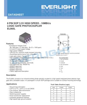
The EL060L is housed in a standard 8-pin Small Outline Package (SOP).
3.1 Pin Configuration and Function
- Pin 1: No Connection (NC)
- Pin 2: Anode (A) of the input infrared LED.
- Pin 3: Cathode (K) of the input infrared LED.
- Pin 4: No Connection (NC)
- Pin 5: Ground (GND) for the output side.
- Pin 6: Output Voltage (VOUT).
- Pin 7: Enable Input (VE). Active high; a logic high (>2.0V) enables the output, a logic low (<0.8V) forces the output high (see Truth Table).
- Pin 8: Supply Voltage (VCC) for the output side (3.3V or 5V).
Critical Design Note: A 0.1μF (or larger) bypass capacitor with good high-frequency characteristics (ceramic or solid tantalum) must be connected between Pin 8 (VCC) and Pin 5 (GND), placed as close as possible to the package pins to ensure stable operation and minimize switching noise.
4. Truth Table and Functional Description
The device operates as a positive logic gate with an enable function. The output state depends on the input (LED) current and the enable pin voltage.
| Input (LED) | Enable (VE) | Output (VOUT) |
|---|---|---|
| H (IF ON) | H (>2.0V) | L (Low) |
| L (IF OFF) | H (>2.0V) | H (High) |
| H (IF ON) | L (<0.8V) | H (High) |
| L (IF OFF) | L (<0.8V) | H (High) |
| H (IF ON) | NC (Floating) | L (Low)* |
| L (IF OFF) | NC (Floating) | H (High)* |
*With the internal pull-up resistor, a floating enable pin defaults to a logic high state.
In essence, when enabled (VE high), the photocoupler acts as an inverter: a lit LED (input high) produces a low output, and an unlit LED (input low) produces a high output. When disabled (VE low), the output is forced high regardless of the input state, which can be useful for tri-state bus control or power-down modes.
5. Application Guidelines and Design Considerations
5.1 Typical Application Circuits
The primary application is digital signal isolation. The input side requires a current-limiting resistor in series with the LED to set the desired IF (e.g., 5-10mA for guaranteed switching). The output side connects directly to the receiving logic gate's input. The enable pin can be tied to VCC if not used, or driven by a control signal for output gating.
5.2 Design Considerations
- Input Drive: Ensure the drive circuit can provide sufficient IF (≥ IFT) across the operating temperature range to guarantee proper output switching. Account for the LED's negative temperature coefficient of VF.
- Power Supply Bypassing: The 0.1μF capacitor on VCC/GND is mandatory for stable high-speed operation and must be placed close to the device.
- Load Considerations: The output can drive up to 10 standard logic inputs (Fan-out 10). Ensure the total capacitive load on the output pin does not significantly exceed the test condition of 15pF to avoid degrading rise/fall times and propagation delays.
- PCB Layout: Maintain good isolation distance between the input (pins 1-4 area) and output (pins 5-8 area) sides on the PCB to preserve the high-voltage isolation rating. Follow creepage and clearance guidelines appropriate for the application's voltage requirements.
6. Compliance and Reliability Information
The EL060L is designed and certified for use in industrial and commercial applications.
- Environmental Compliance: The device is Halogen Free (Br <900ppm, Cl <900ppm, Br+Cl <1500ppm), Pb-free, and compliant with the RoHS (Restriction of Hazardous Substances) directive and EU REACH regulations.
- Safety Approvals: It carries approvals from major international safety agencies:
- UL (Underwriters Laboratories) and cUL (File No. E214129)
- VDE (Verband der Elektrotechnik) (File No. 40028116)
- SEMKO, NEMKO, DEMKO, FIMKO (Nordic safety agencies)
- Reliability: Performance is guaranteed over the extended industrial temperature range of -40°C to +85°C.
7. Test Circuits and Waveform Definitions
The datasheet includes standard test circuits for characterizing switching parameters.
- Fig. 12: Defines the test setup and measurement points for propagation delays (tPHL, tPLH) and output transition times (tr, tf). Delays are measured between the 3.75mA point on the input current waveform and the 1.5V point on the output voltage waveform.
- Fig. 13: Defines the test setup for enable propagation delays (tEHL, tELH), measured from the 1.5V point on the enable input.
- Fig. 14: Illustrates the test circuit for Common-Mode Transient Immunity (CMTI), applying a high-voltage differential pulse (VCM) between the input and output grounds to measure noise immunity.
8. Soldering and Handling
The device is suitable for standard surface-mount assembly processes.
- Reflow Soldering: The maximum peak soldering temperature is 260°C, as per the IPC/JEDEC J-STD-020 standard for lead-free assemblies. The device should not be exposed to this temperature for more than 10 seconds.
- Storage: Store in a dry, anti-static environment within the specified storage temperature range of -55°C to +125°C.
- ESD Precautions: Standard ESD (Electrostatic Discharge) precautions should be observed during handling, as with all semiconductor devices.
9. Technical Comparison and Positioning
The EL060L positions itself in the market as a general-purpose, high-speed digital isolator. Its key differentiators are the combination of 10Mbit/s speed, dual 3.3V/5V supply compatibility, and the inclusion of an enable/strobe function in a standard SOP-8 package. Compared to simpler 4-pin photocouplers, it offers the added control of the enable pin. Compared to newer, specialized digital isolator ICs based on capacitive or magnetic coupling, it offers the proven reliability, high CMTI, and simplicity of optocoupler technology, often at a lower cost for applications not requiring extreme speeds (>>10Mbit/s).
10. Frequently Asked Questions (FAQ)
Q: Can I use a 5V supply for VCC?
A: Yes, the device is designed for dual 3.3V and 5V supply operation. Ensure the bypass capacitor voltage rating is sufficient for 5V.
Q: Is an external pull-up resistor needed on the Enable (VE) pin?
A: No. The device incorporates an internal pull-up resistor, as noted in the datasheet.
Q: What is the purpose of the enable pin?
A: It allows the output to be forced high, effectively disabling the signal path. This is useful for putting a bus interface into a high-impedance state, implementing power-saving modes, or multiplexing multiple isolator outputs.
Q: How do I calculate the input series resistor (RIN)?
A: RIN = (VDRIVE - VF) / IF. Use VF(max) at the lowest operating temperature for a conservative design to ensure minimum IF is met. For example, with a 5V drive, VF=1.8V, and IF=7.5mA: RIN = (5 - 1.8) / 0.0075 ≈ 427Ω. Use the nearest standard value (e.g., 430Ω).
Q: What does "Fan out 10" mean?
A: It means the output can reliably drive the inputs of up to 10 standard digital logic gates (e.g., 74HC series) connected in parallel, while maintaining valid logic voltage levels.
LED Specification Terminology
Complete explanation of LED technical terms
Photoelectric Performance
| Term | Unit/Representation | Simple Explanation | Why Important |
|---|---|---|---|
| Luminous Efficacy | lm/W (lumens per watt) | Light output per watt of electricity, higher means more energy efficient. | Directly determines energy efficiency grade and electricity cost. |
| Luminous Flux | lm (lumens) | Total light emitted by source, commonly called "brightness". | Determines if the light is bright enough. |
| Viewing Angle | ° (degrees), e.g., 120° | Angle where light intensity drops to half, determines beam width. | Affects illumination range and uniformity. |
| CCT (Color Temperature) | K (Kelvin), e.g., 2700K/6500K | Warmth/coolness of light, lower values yellowish/warm, higher whitish/cool. | Determines lighting atmosphere and suitable scenarios. |
| CRI / Ra | Unitless, 0–100 | Ability to render object colors accurately, Ra≥80 is good. | Affects color authenticity, used in high-demand places like malls, museums. |
| SDCM | MacAdam ellipse steps, e.g., "5-step" | Color consistency metric, smaller steps mean more consistent color. | Ensures uniform color across same batch of LEDs. |
| Dominant Wavelength | nm (nanometers), e.g., 620nm (red) | Wavelength corresponding to color of colored LEDs. | Determines hue of red, yellow, green monochrome LEDs. |
| Spectral Distribution | Wavelength vs intensity curve | Shows intensity distribution across wavelengths. | Affects color rendering and quality. |
Electrical Parameters
| Term | Symbol | Simple Explanation | Design Considerations |
|---|---|---|---|
| Forward Voltage | Vf | Minimum voltage to turn on LED, like "starting threshold". | Driver voltage must be ≥Vf, voltages add up for series LEDs. |
| Forward Current | If | Current value for normal LED operation. | Usually constant current drive, current determines brightness & lifespan. |
| Max Pulse Current | Ifp | Peak current tolerable for short periods, used for dimming or flashing. | Pulse width & duty cycle must be strictly controlled to avoid damage. |
| Reverse Voltage | Vr | Max reverse voltage LED can withstand, beyond may cause breakdown. | Circuit must prevent reverse connection or voltage spikes. |
| Thermal Resistance | Rth (°C/W) | Resistance to heat transfer from chip to solder, lower is better. | High thermal resistance requires stronger heat dissipation. |
| ESD Immunity | V (HBM), e.g., 1000V | Ability to withstand electrostatic discharge, higher means less vulnerable. | Anti-static measures needed in production, especially for sensitive LEDs. |
Thermal Management & Reliability
| Term | Key Metric | Simple Explanation | Impact |
|---|---|---|---|
| Junction Temperature | Tj (°C) | Actual operating temperature inside LED chip. | Every 10°C reduction may double lifespan; too high causes light decay, color shift. |
| Lumen Depreciation | L70 / L80 (hours) | Time for brightness to drop to 70% or 80% of initial. | Directly defines LED "service life". |
| Lumen Maintenance | % (e.g., 70%) | Percentage of brightness retained after time. | Indicates brightness retention over long-term use. |
| Color Shift | Δu′v′ or MacAdam ellipse | Degree of color change during use. | Affects color consistency in lighting scenes. |
| Thermal Aging | Material degradation | Deterioration due to long-term high temperature. | May cause brightness drop, color change, or open-circuit failure. |
Packaging & Materials
| Term | Common Types | Simple Explanation | Features & Applications |
|---|---|---|---|
| Package Type | EMC, PPA, Ceramic | Housing material protecting chip, providing optical/thermal interface. | EMC: good heat resistance, low cost; Ceramic: better heat dissipation, longer life. |
| Chip Structure | Front, Flip Chip | Chip electrode arrangement. | Flip chip: better heat dissipation, higher efficacy, for high-power. |
| Phosphor Coating | YAG, Silicate, Nitride | Covers blue chip, converts some to yellow/red, mixes to white. | Different phosphors affect efficacy, CCT, and CRI. |
| Lens/Optics | Flat, Microlens, TIR | Optical structure on surface controlling light distribution. | Determines viewing angle and light distribution curve. |
Quality Control & Binning
| Term | Binning Content | Simple Explanation | Purpose |
|---|---|---|---|
| Luminous Flux Bin | Code e.g., 2G, 2H | Grouped by brightness, each group has min/max lumen values. | Ensures uniform brightness in same batch. |
| Voltage Bin | Code e.g., 6W, 6X | Grouped by forward voltage range. | Facilitates driver matching, improves system efficiency. |
| Color Bin | 5-step MacAdam ellipse | Grouped by color coordinates, ensuring tight range. | Guarantees color consistency, avoids uneven color within fixture. |
| CCT Bin | 2700K, 3000K etc. | Grouped by CCT, each has corresponding coordinate range. | Meets different scene CCT requirements. |
Testing & Certification
| Term | Standard/Test | Simple Explanation | Significance |
|---|---|---|---|
| LM-80 | Lumen maintenance test | Long-term lighting at constant temperature, recording brightness decay. | Used to estimate LED life (with TM-21). |
| TM-21 | Life estimation standard | Estimates life under actual conditions based on LM-80 data. | Provides scientific life prediction. |
| IESNA | Illuminating Engineering Society | Covers optical, electrical, thermal test methods. | Industry-recognized test basis. |
| RoHS / REACH | Environmental certification | Ensures no harmful substances (lead, mercury). | Market access requirement internationally. |
| ENERGY STAR / DLC | Energy efficiency certification | Energy efficiency and performance certification for lighting. | Used in government procurement, subsidy programs, enhances competitiveness. |