1. Product Overview
The ELM8XL-G Series represents a family of high-speed, logic gate output photocouplers (optoisolators) designed for modern digital isolation applications. The core function of this device is to provide galvanic isolation between input and output circuits while transmitting digital logic signals at high speeds. It integrates an infrared light-emitting diode (LED) on the input side, which is optically coupled to a CMOS detector integrated circuit on the output side. This optical coupling method eliminates electrical connection, providing high voltage isolation and noise immunity, which is critical in systems with different ground potentials or in noisy electrical environments.
The device is packaged in a compact, surface-mount 5-pin Small Outline Package (SOP), making it suitable for automated assembly processes and space-constrained PCB designs. Its primary design goal is to facilitate reliable, high-speed data transmission across isolation barriers, serving as a direct replacement for pulse transformers in many applications while offering advantages in size, cost, and integration.
1.1 Core Advantages and Target Market
The ELM8XL-G Series offers several key advantages that define its position in the market. First is its high-speed capability, supporting data rates up to 15 Megabits per second (MBit/s). This makes it suitable for modern communication interfaces and fast control signals. Second is its dual supply voltage compatibility, functioning correctly with both 3.3V and 5V CMOS logic levels, which provides design flexibility for mixed-voltage systems. Third is its high isolation rating of 3750 Vrms, ensuring safety and reliability in applications requiring protection from high voltage transients or differences in ground potential.
The device is also manufactured to meet stringent environmental and safety standards. It is halogen-free (with Bromine <900ppm, Chlorine <900ppm, Br+Cl <1500ppm), compliant with EU REACH regulations, and is both Pb-free and RoHS compliant. It carries approvals from major international safety agencies including UL, cUL, VDE, SEMKO, NEMKO, DEMKO, and FIMKO, which is essential for products targeting global markets, particularly in industrial, telecommunications, and computing equipment.
The target applications are diverse and center around the need for signal isolation:
- Line Receivers and Data Transmission: Isolating serial communication lines (RS-232, RS-485, etc.) to prevent ground loops and noise.
- Data Multiplexing: Providing isolation in multiplexed data bus systems.
- Switching Power Supplies: Isolating feedback signals in flyback or other isolated converter topologies.
- Pulse Transformer Replacement: Offering a smaller, more integrated solution for signal isolation traditionally done with transformers.
- Computer Peripheral Interfaces: Isolating signals to/from printers, industrial I/O, and other peripherals.
- High-Speed Logic Ground Isolation: Separating digital grounds between subsystems, such as between a microcontroller and motor drivers, to prevent noise coupling.
2. In-Depth Technical Parameter Analysis
A thorough understanding of the electrical and switching characteristics is crucial for successful implementation of the ELM8XL-G photocoupler in a circuit design.
2.1 Absolute Maximum Ratings
These ratings define the stress limits beyond which permanent damage to the device may occur. Operation under these conditions is not guaranteed and should be avoided.
- Input Forward Current (IF): 15 mA maximum. The current driving the internal LED must not exceed this value.
- Input Reverse Voltage (VR): 5 V maximum. The reverse voltage applied across the LED must be limited.
- Input Power Dissipation (PD): 35 mW maximum for the input side.
- Output Power Dissipation (PO): 85 mW maximum for the output CMOS IC.
- Output Current (IO): 20 mA maximum sink/source current from the output pin.
- Supply Voltage (VCC): 5.5 V maximum. This is the absolute maximum voltage that can be applied to the output side's power pin.
- Total Power Dissipation (PT): 100 mW maximum for the entire device.
- Isolation Voltage (VISO): 3750 Vrms for 1 minute. This is a safety rating tested under specific conditions (pins 1 & 3 shorted, pins 4, 5 & 6 shorted) at 40-60% relative humidity.
- Operating Temperature (TOPR): -40°C to +85°C. The device is guaranteed to meet its published specifications within this range.
- Storage Temperature (TSTG): -55°C to +125°C.
- Soldering Temperature (TSOL): 260°C for 10 seconds, compliant with typical lead-free reflow profiles.
Design Note: The datasheet specifies that the VCC supply must be bypassed with a 0.1µF or larger capacitor (ceramic or solid tantalum with good high-frequency characteristics) placed as close as possible to the device's VCC and GND pins. This is critical for stable operation and noise immunity of the high-speed CMOS output stage.
2.2 Electrical Characteristics
These parameters define the guaranteed performance of the device under normal operating conditions (TA=25°C unless noted).
2.2.1 Input Characteristics (LED Side)
- Forward Voltage (VF): Typically 1.4V, with a maximum of 1.8V at a forward current (IF) of 8mA. This is used to calculate the required current-limiting resistor value on the input side: Rlimit = (Vsupply - VF) / IF.
- Reverse Voltage (VR): 5.0V minimum. The LED can withstand up to 5V in reverse bias.
- Temperature Coefficient of VF (ΔVF/ΔTA): Approximately -1.7 mV/°C. The forward voltage drops slightly as temperature increases.
- Input Capacitance (CIN): Typically 60 pF. This affects the high-frequency response of the input drive circuit.
2.2.2 Output Characteristics (CMOS IC Side)
- Supply Current (ICCH, ICCL): Typically 1.3mA, with a maximum of 6mA, whether the output is in a high (IF=0mA) or low (IF=8mA) state. This is the quiescent current drawn by the output IC from VCC.
- High-Level Output Voltage (VOH): For a 3.3V supply, VOH is guaranteed to be at least VCC - 1V (i.e., 2.3V) and is typically VCC - 0.3V (3.0V) when sinking 4mA. For a 5V supply, it's VCC - 1V (4.0V) min, typically VCC - 0.2V (4.8V). This ensures solid logic-high levels.
- Low-Level Output Voltage (VOL): For a 3.3V supply, VOL is typically 0.21V with a maximum of 0.6V when sourcing 4mA (IF=8mA). For a 5V supply, it's typically 0.17V, max 0.6V. This ensures solid logic-low levels.
- Input Threshold Current (IFT): The LED current required to guarantee a logic-low output. It is typically 2.5mA (max 5mA) at VCC=3.3V with a very light load (IOL=20µA). The design should use an IF well above this (e.g., 8mA as shown in test conditions) for reliable switching and noise margin.
2.3 Switching Characteristics
These parameters define the timing performance, which is critical for high-speed data transmission.
- Propagation Delay to Output High (tPHL): The time from the input LED turning OFF (IF going from 8mA to 0mA) to the output reaching a valid logic HIGH. Typical is 30ns (max 65ns) at VCC=3.3V, and 33ns typical at VCC=5V.
- Propagation Delay to Output Low (tPLH): The time from the input LED turning ON (IF going from 0mA to 8mA) to the output reaching a valid logic LOW. Typical is 48ns (max 65ns) at VCC=3.3V, and 52ns typical at VCC=5V.
- Pulse Width Distortion (|tPHL – tPLH|): The absolute difference between the two propagation delays. This is crucial for maintaining the integrity of pulse widths. It is typically 20ns (max 50ns) at 3.3V and 22ns typical at 5V. A lower value is better.
- Output Rise/Fall Time (tr, tf): Typically 7ns each. This defines the edge speed of the output signal.
- Common Mode Transient Immunity (CMTI): This is a key isolation parameter. It measures the device's ability to ignore fast voltage transients between the input and output grounds. Two grades are specified: M80L with a minimum of 5,000 V/µs, and M81L with a minimum of 10,000 V/µs. This is tested with a 1000V peak-to-peak common-mode voltage (VCM) and ensures the output state does not falsely toggle due to noise.
3. Mechanical and Packaging Information
3.1 Pin Configuration and Truth Table
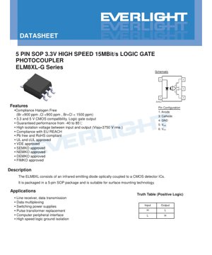
The device uses a 5-pin SOP package, though six pin numbers are referenced (1-6, with pin 2 presumably being No Connect or an internal connection). The functional pins are:
- Pin 1: Anode of the input LED.
- Pin 3: Cathode of the input LED.
- Pin 4: GND for the output CMOS IC.
- Pin 5: VOUT, the digital output signal.
- Pin 6: VCC, the supply voltage (3.3V or 5V) for the output CMOS IC.
The device implements a non-inverting logic gate function (Positive Logic):
- Input HIGH (LED ON, IF > IFT): Output = LOW
- Input LOW (LED OFF, IF = 0): Output = HIGH
This is a current-sinking input; a current must be driven into the LED to produce a low output.
3.2 Package Dimensions and PCB Layout
The datasheet provides detailed mechanical drawings for the 5-pin SOP package. Key dimensions include the body size, lead pitch, and standoff height. A recommended pad layout for surface mounting is also provided. This layout is designed to ensure reliable solder joint formation during reflow soldering. The datasheet notes that these pad dimensions are suggestions and may need modification based on specific PCB manufacturing processes or thermal requirements, but they serve as an excellent starting point for design.
3.3 Device Marking
The top of the package is marked with a laser or ink code for identification. The marking follows the format: EL M81L YWW V.
- EL: Manufacturer code.
- M81L: Device number (specific to the CMTI grade and variant).
- Y: One-digit year code.
- WW: Two-digit week code.
- V: Optional marking indicating VDE approval.
4. Application Guidelines and Design Considerations
4.1 Input Circuit Design
The input circuit must provide a controlled current to the LED. A simple series resistor is sufficient. The value is calculated based on the driving voltage and the desired IF. For example, to drive IF = 8mA from a 5V logic signal with a typical VF of 1.4V: Rlimit = (5V - 1.4V) / 0.008A = 450Ω. A standard 470Ω resistor would be suitable. Ensure the driving source can provide the necessary current. For driving from a microcontroller GPIO pin, verify the pin's current sourcing capability. If insufficient, a simple transistor buffer (e.g., an NPN or N-channel MOSFET) may be required.
4.2 Output Circuit Design
The output is a standard CMOS digital output. It can directly drive CMOS, TTL, or LVCMOS inputs. The key requirements are:
- Power Supply Bypassing: As stressed in the datasheet, a 0.1µF ceramic capacitor must be placed directly between Pin 6 (VCC) and Pin 4 (GND). This is non-negotiable for stable high-speed operation and preventing noise on the output.
- Load Considerations: The output can sink/source up to 20mA, but for best speed and signal integrity, loads should be primarily capacitive (e.g., the input capacitance of another gate). Driving heavy resistive loads or long traces will increase rise/fall times and may affect timing margins.
- Pull-up Resistors: Not required, as the output actively drives both high and low states.
4.3 Speed and Timing Considerations
For a 15 MBit/s data rate, the bit period is approximately 66.7ns. The total signal delay through the photocoupler is the sum of tPLH or tPHL plus a portion of the rise/fall time. With typical delays around 30-50ns, there is adequate margin for this data rate. However, the pulse width distortion is important. A distortion of 20ns means a pulse will be narrowed or widened by that amount after passing through the isolator. For very narrow pulses, this could cause them to disappear if the distortion is greater than the pulse width. Always consider the maximum, not typical, values for timing-critical designs.
4.4 Isolation and Safety Design
The 3750Vrms isolation rating is a safety requirement. To maintain this rating in the end product, PCB layout is critical. Ensure that the creepage and clearance distances on the PCB between all input-side traces/components and output-side traces/components meet or exceed the requirements for the system's working isolation voltage (which is lower than the 3750Vrms test voltage). This often means incorporating a wide slot or barrier in the PCB under the photocoupler package. Consult relevant safety standards (e.g., IEC 60950, IEC 61010) for specific distance requirements based on voltage, pollution degree, and material group.
5. Ordering Information and Packaging
The part number follows the structure: ELM8XL(Z)-V.
- ELM8XL: Base part number.
- (Z): Tape and reel option. Can be "TA", "TB", or omitted for tube packaging.
- -V: Optional suffix denoting VDE approval is included.
Packaging Options:
- Tube: 100 units per tube. Standard for manual or low-volume assembly.
- Tape and Reel (TA or TB): 3000 units per reel. The "TA" and "TB"> likely refer to different reel sizes or tape widths (e.g., 8mm vs. 12mm). This option is for automated pick-and-place assembly.
The datasheet includes detailed tape and reel specifications, including pocket dimensions (A, B, D0, D1), pitch (P0, P1, P2), tape thickness (t), and reel width (W). These dimensions are essential for programming the feeder on an automated assembly machine.
6. Performance Curves and Typical Characteristics
While the PDF excerpt mentions "Typical Electro-Optical Characteristics Curves," the specific graphs are not included in the provided text. Typically, such datasheets include curves showing:
- Forward Current (IF) vs. Forward Voltage (VF): Shows the diode-like characteristic of the input LED at different temperatures.
- Current Transfer Ratio (CTR) vs. Forward Current: Although this is a digital device, a form of CTR exists—the relationship between IF and the resulting output state. The threshold current IFT is the key parameter.
- Propagation Delay vs. Supply Voltage (VCC): How timing parameters change with VCC.
- Propagation Delay vs. Temperature: How timing parameters change over the operating temperature range.
- Supply Current (ICC) vs. Temperature: Variation of quiescent current with temperature.
Designers should use the minimum and maximum values from the tables for robust design, using the typical curves only for understanding trends and behaviors.
7. Comparison and Technology Context
The ELM8XL-G sits in a category of high-speed digital photocouplers. Compared to older photocouplers with transistor or Darlington outputs, its CMOS logic gate output provides much faster switching speeds, sharper edges, and well-defined logic levels. Compared to pulse transformers, it offers a smaller footprint, DC coupling capability (transformers cannot pass DC signals), and often lower cost. Compared to newer isolation technologies like capacitive (digital isolators) or giant magnetoresistive (GMR) isolators, photocouplers like the ELM8XL-G offer the advantage of proven reliability, very high intrinsic isolation strength, and immunity to magnetic fields. The trade-off is generally slower speed and higher power consumption (due to the LED drive current) than the latest semiconductor-based isolators. The choice depends on the specific application requirements for speed, power, cost, and noise immunity.
8. Frequently Asked Questions (FAQ)
Q: Can I use this with a 3.3V input signal to drive the LED?
A: Yes, but you must recalculate the current-limiting resistor. For a 3.3V drive and VF~1.4V, to get IF=8mA, R = (3.3V - 1.4V) / 0.008A = 237.5Ω. Use a 240Ω resistor. Ensure the 3.3V source can provide 8mA.
Q: What is the difference between the M80L and M81L versions?
A: The primary difference is the Common Mode Transient Immunity (CMTI). The M81L version guarantees a minimum of 10,000 V/µs, while the M80L guarantees 5,000 V/µs. Choose the M81L for noisier environments, such as motor drives or industrial power systems.
Q: Is an external pull-up resistor needed on the output?
A: No. The output is an active push-pull CMOS stage that drives both high and low levels. An external pull-up is unnecessary and would only increase power consumption.
Q: How do I ensure the high isolation rating is maintained in my PCB design?
A: You must maintain adequate creepage (distance along the surface) and clearance (air gap) between all conductors on the input side and all conductors on the output side. This typically requires a physical gap or slot in the PCB underneath the photocoupler body. The specific distances depend on your application's working voltage and the safety standards it must meet.
Q: Can the output pin (5) be connected directly to another device's input, or do I need a series resistor?
A: It can be connected directly. The output is designed to drive standard digital inputs. A series resistor is generally not needed and would slow down the signal edges.
LED Specification Terminology
Complete explanation of LED technical terms
Photoelectric Performance
| Term | Unit/Representation | Simple Explanation | Why Important |
|---|---|---|---|
| Luminous Efficacy | lm/W (lumens per watt) | Light output per watt of electricity, higher means more energy efficient. | Directly determines energy efficiency grade and electricity cost. |
| Luminous Flux | lm (lumens) | Total light emitted by source, commonly called "brightness". | Determines if the light is bright enough. |
| Viewing Angle | ° (degrees), e.g., 120° | Angle where light intensity drops to half, determines beam width. | Affects illumination range and uniformity. |
| CCT (Color Temperature) | K (Kelvin), e.g., 2700K/6500K | Warmth/coolness of light, lower values yellowish/warm, higher whitish/cool. | Determines lighting atmosphere and suitable scenarios. |
| CRI / Ra | Unitless, 0–100 | Ability to render object colors accurately, Ra≥80 is good. | Affects color authenticity, used in high-demand places like malls, museums. |
| SDCM | MacAdam ellipse steps, e.g., "5-step" | Color consistency metric, smaller steps mean more consistent color. | Ensures uniform color across same batch of LEDs. |
| Dominant Wavelength | nm (nanometers), e.g., 620nm (red) | Wavelength corresponding to color of colored LEDs. | Determines hue of red, yellow, green monochrome LEDs. |
| Spectral Distribution | Wavelength vs intensity curve | Shows intensity distribution across wavelengths. | Affects color rendering and quality. |
Electrical Parameters
| Term | Symbol | Simple Explanation | Design Considerations |
|---|---|---|---|
| Forward Voltage | Vf | Minimum voltage to turn on LED, like "starting threshold". | Driver voltage must be ≥Vf, voltages add up for series LEDs. |
| Forward Current | If | Current value for normal LED operation. | Usually constant current drive, current determines brightness & lifespan. |
| Max Pulse Current | Ifp | Peak current tolerable for short periods, used for dimming or flashing. | Pulse width & duty cycle must be strictly controlled to avoid damage. |
| Reverse Voltage | Vr | Max reverse voltage LED can withstand, beyond may cause breakdown. | Circuit must prevent reverse connection or voltage spikes. |
| Thermal Resistance | Rth (°C/W) | Resistance to heat transfer from chip to solder, lower is better. | High thermal resistance requires stronger heat dissipation. |
| ESD Immunity | V (HBM), e.g., 1000V | Ability to withstand electrostatic discharge, higher means less vulnerable. | Anti-static measures needed in production, especially for sensitive LEDs. |
Thermal Management & Reliability
| Term | Key Metric | Simple Explanation | Impact |
|---|---|---|---|
| Junction Temperature | Tj (°C) | Actual operating temperature inside LED chip. | Every 10°C reduction may double lifespan; too high causes light decay, color shift. |
| Lumen Depreciation | L70 / L80 (hours) | Time for brightness to drop to 70% or 80% of initial. | Directly defines LED "service life". |
| Lumen Maintenance | % (e.g., 70%) | Percentage of brightness retained after time. | Indicates brightness retention over long-term use. |
| Color Shift | Δu′v′ or MacAdam ellipse | Degree of color change during use. | Affects color consistency in lighting scenes. |
| Thermal Aging | Material degradation | Deterioration due to long-term high temperature. | May cause brightness drop, color change, or open-circuit failure. |
Packaging & Materials
| Term | Common Types | Simple Explanation | Features & Applications |
|---|---|---|---|
| Package Type | EMC, PPA, Ceramic | Housing material protecting chip, providing optical/thermal interface. | EMC: good heat resistance, low cost; Ceramic: better heat dissipation, longer life. |
| Chip Structure | Front, Flip Chip | Chip electrode arrangement. | Flip chip: better heat dissipation, higher efficacy, for high-power. |
| Phosphor Coating | YAG, Silicate, Nitride | Covers blue chip, converts some to yellow/red, mixes to white. | Different phosphors affect efficacy, CCT, and CRI. |
| Lens/Optics | Flat, Microlens, TIR | Optical structure on surface controlling light distribution. | Determines viewing angle and light distribution curve. |
Quality Control & Binning
| Term | Binning Content | Simple Explanation | Purpose |
|---|---|---|---|
| Luminous Flux Bin | Code e.g., 2G, 2H | Grouped by brightness, each group has min/max lumen values. | Ensures uniform brightness in same batch. |
| Voltage Bin | Code e.g., 6W, 6X | Grouped by forward voltage range. | Facilitates driver matching, improves system efficiency. |
| Color Bin | 5-step MacAdam ellipse | Grouped by color coordinates, ensuring tight range. | Guarantees color consistency, avoids uneven color within fixture. |
| CCT Bin | 2700K, 3000K etc. | Grouped by CCT, each has corresponding coordinate range. | Meets different scene CCT requirements. |
Testing & Certification
| Term | Standard/Test | Simple Explanation | Significance |
|---|---|---|---|
| LM-80 | Lumen maintenance test | Long-term lighting at constant temperature, recording brightness decay. | Used to estimate LED life (with TM-21). |
| TM-21 | Life estimation standard | Estimates life under actual conditions based on LM-80 data. | Provides scientific life prediction. |
| IESNA | Illuminating Engineering Society | Covers optical, electrical, thermal test methods. | Industry-recognized test basis. |
| RoHS / REACH | Environmental certification | Ensures no harmful substances (lead, mercury). | Market access requirement internationally. |
| ENERGY STAR / DLC | Energy efficiency certification | Energy efficiency and performance certification for lighting. | Used in government procurement, subsidy programs, enhances competitiveness. |