Table of Contents
- 1. Product Overview
- 2. Key Features and Applications
- 2.1 Core Advantages
- 2.2 Target Applications
- 3. Technical Parameter Analysis
- 3.1 Absolute Maximum Ratings
- 3.2 Electro-Optical Characteristics (Ta=25°C)
- 4. Performance Curve Analysis
- 4.1 Spectral Sensitivity (Fig. 1)
- 4.2 Reverse Light Current vs. Irradiance (Fig. 2)
- 5. Mechanical and Packaging Information
- 5.1 Package Dimensions
- 5.2 Polarity Identification
- 5.3 Carrier Tape and Reel Specifications
- 6. Soldering and Assembly Guidelines
- 6.1 Storage and Moisture Sensitivity
- 6.2 Reflow Soldering Profile
- 6.3 Hand Soldering and Rework
- 6.4 Circuit Board Design Considerations
- 7. Application Design Considerations
- 7.1 Over-Current Protection
- 7.2 Biasing and Interface Circuitry
- 7.3 Optical Design
- 8. Technical Comparison and Selection
- 9. Operational Principles
- 10. Disclaimer and Usage Notes
- LED Specification Terminology
- Photoelectric Performance
- Electrical Parameters
- Thermal Management & Reliability
- Packaging & Materials
- Quality Control & Binning
- Testing & Certification
1. Product Overview
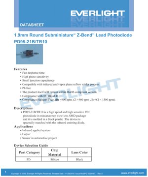
The PD95-21B/TR10 is a subminiature, surface-mount device (SMD) designed for high-performance light sensing applications. It is a silicon-based PIN photodiode, which is a fundamental semiconductor component that converts light energy into electrical current. The device is housed in a compact, 1.9mm diameter round package with a distinctive "Z-Bend" lead configuration, making it suitable for automated assembly processes. The top of the package features a black plastic lens that helps define the field of view and provides some environmental protection. Its primary function is to detect infrared radiation, with its spectral characteristics specifically tuned to match common infrared emitting diodes (IREDs), making it an ideal receiver component in optoelectronic systems.
2. Key Features and Applications
2.1 Core Advantages
The photodiode offers several performance benefits crucial for modern electronic design:
- Fast Response Time: The PIN structure, with its intrinsic (I) region, allows for rapid carrier collection, enabling the device to respond quickly to changes in light intensity. This is essential for data communication, pulse detection, and high-speed sensing.
- High Photo Sensitivity: It efficiently generates a measurable electrical current from low levels of incident light (irradiance), improving signal-to-noise ratio in detection circuits.
- Small Junction Capacitance: A low capacitance is critical for maintaining high bandwidth and fast response, as it minimizes the RC time constant of the detection circuit.
- Robust Manufacturing Compatibility: The device is designed to withstand standard infrared and vapor phase reflow soldering processes, facilitating reliable PCB assembly.
- Environmental Compliance: The component is lead-free (Pb-free), compliant with the EU's REACH regulation, and meets halogen-free requirements (Br <900 ppm, Cl <900 ppm, Br+Cl <1500 ppm), aligning with global environmental and safety standards.
2.2 Target Applications
This photodiode is engineered for systems requiring reliable infrared detection. Typical application areas include:
- Infrared Applied Systems: This encompasses a wide range, including remote controls, proximity sensors, object detection, and interruptive optical switches.
- Copiers and Printers: Used for paper detection, toner level sensing, and scanning mechanisms where precise detection of reflected or transmitted light is needed.
- Automotive Sensors: Suitable for non-critical sensing projects within vehicles, such as rain sensors, twilight sensors, or interior occupancy detection, where reliability across a temperature range is important.
3. Technical Parameter Analysis
3.1 Absolute Maximum Ratings
These limits define the stress conditions beyond which permanent damage may occur. Operation should always be within these bounds.
- Reverse Voltage (VR): 32 V. The maximum voltage that can be applied in reverse bias across the diode without causing breakdown.
- Operating Temperature (Topr): -25°C to +85°C. The ambient temperature range over which the device is specified to function correctly.
- Storage Temperature (Tstg): -40°C to +85°C. The temperature range for non-operational storage.
- Soldering Temperature (Tsol): 260°C for a maximum of 5 seconds. This defines the peak temperature tolerance during reflow soldering.
- Power Dissipation (Pd): 150 mW at 25°C. The maximum power the device can safely dissipate as heat.
3.2 Electro-Optical Characteristics (Ta=25°C)
These parameters define the device's performance under typical operating conditions.
- Spectral Bandwidth (λ0.5): 730 nm to 1100 nm. This is the wavelength range where the photodiode's responsivity is at least half of its peak value. It confirms the device is sensitive across the near-infrared spectrum.
- Peak Sensitivity Wavelength (λP): 940 nm (Typical). The wavelength of light at which the photodiode is most sensitive. This aligns perfectly with the emission peak of many standard GaAlAs infrared LEDs.
- Short-Circuit Current (ISC): 4 µA (Typical) at Ee=1 mW/cm², λ=875 nm. The current generated when the photodiode terminals are short-circuited (zero bias voltage). It is a direct measure of photocurrent generation efficiency.
- Reverse Light Current (IL): 4 µA (Typical) at Ee=1 mW/cm², λ=875 nm, VR=5V. The current flowing under reverse bias when illuminated. Operating in reverse bias (photoconductive mode) generally offers faster response and more linear output than zero-bias (photovoltaic mode).
- Reverse Dark Current (ID): 10 nA (Max) at VR=10V. The small leakage current that flows under reverse bias conditions in complete darkness. A low dark current is critical for detecting weak light signals, as it represents the noise floor of the device.
- Reverse Breakdown Voltage (VBR): 32 V (Min), 170 V (Typical). The voltage at which the reverse current increases sharply. The device should never be operated near this point.
4. Performance Curve Analysis
The datasheet references typical performance curves which provide deeper insight than single-point specifications.
4.1 Spectral Sensitivity (Fig. 1)
This curve graphically represents the photodiode's responsivity as a function of the wavelength of incident light. It will show a bell-shaped curve, peaking at approximately 940 nm and tapering off towards the specified 730 nm and 1100 nm points at half the peak sensitivity. This curve is essential for matching the photodiode to a specific light source, ensuring maximum signal strength.
4.2 Reverse Light Current vs. Irradiance (Fig. 2)
This plot illustrates the relationship between the generated photocurrent (IL) and the incident light power density (Ee). For a well-designed PIN photodiode operating in its linear region, this relationship should be highly linear. The slope of this line represents the photodiode's responsivity (typically in A/W). This linearity is crucial for analog light measurement applications.
5. Mechanical and Packaging Information
5.1 Package Dimensions
The device is a 1.9mm diameter round package. Detailed mechanical drawings are provided in the datasheet, specifying all critical dimensions including body diameter, height, lead spacing, and lead dimensions. All dimensions are in millimeters with a standard tolerance of ±0.1mm unless otherwise noted. The "Z-Bend" lead style is designed to provide a stable footprint for surface mounting and relieve mechanical stress.
5.2 Polarity Identification
The photodiode is a polarized component. The datasheet drawing clearly indicates the cathode and anode terminals. Correct polarity must be observed during circuit board assembly for proper operation in reverse-bias configuration.
5.3 Carrier Tape and Reel Specifications
For automated assembly, the components are supplied in carrier tape and reel. The datasheet includes the dimensions for the carrier tape pockets, reel diameter, and orientation. The standard packing quantity is 1000 pieces per reel.
6. Soldering and Assembly Guidelines
6.1 Storage and Moisture Sensitivity
The photodiode is moisture-sensitive. Precautions must be taken to prevent popcorning or delamination during reflow soldering:
- Store unopened bags at ≤30°C and ≤90% RH.
- Use components within one year.
- After opening, store at ≤30°C and ≤70% RH.
- Use within 168 hours (7 days) after opening the moisture barrier bag.
- If the storage time is exceeded or the desiccant indicates moisture ingress, bake at 60±5°C for 24 hours before use.
6.2 Reflow Soldering Profile
A lead-free reflow soldering temperature profile is recommended. The profile should be controlled to ensure the peak body temperature does not exceed 260°C for more than 5 seconds. Reflow soldering should not be performed more than two times to avoid thermal damage to the plastic package and semiconductor die.
6.3 Hand Soldering and Rework
If hand soldering is necessary, extreme care is required:
- Use a soldering iron with a temperature below 350°C and a power rating below 25W.
- Limit contact time per lead to 3 seconds.
- Allow a cooling interval of at least 2 seconds between soldering each lead.
- Avoid mechanical stress on the component during heating.
- Rework is strongly discouraged. If unavoidable, a specialized dual-head soldering iron should be used to simultaneously heat both leads, preventing thermal stress. The device's functionality must be verified after any rework attempt.
6.4 Circuit Board Design Considerations
After soldering, the circuit board should not be warped or bent, as this can transfer stress to the brittle semiconductor die or solder joints, potentially causing failure.
7. Application Design Considerations
7.1 Over-Current Protection
A critical design note: The photodiode itself does not have internal current limiting. When operated in reverse bias, even a small increase in voltage can cause a large, potentially destructive increase in current if the device is exposed to light. Therefore, an external series resistor must be used in the bias circuit to limit the maximum current under bright illumination conditions and prevent burnout.
7.2 Biasing and Interface Circuitry
The photodiode can be used in two primary modes:
- Photoconductive Mode (Reverse Bias): Applying a reverse bias voltage (e.g., 5V as in the test condition) widens the depletion region, reducing junction capacitance and speeding up the response time. This is the preferred mode for high-speed and linear applications. The output is a current source, typically converted to a voltage using a transimpedance amplifier (TIA).
- Photovoltaic Mode (Zero Bias): The photodiode generates its own voltage when illuminated, operating like a solar cell. This mode offers very low dark current but has slower response and less linearity. It is suitable for low-frequency light measurement where simplicity is key.
7.3 Optical Design
The black lens provides a defined viewing angle. For optimal performance, the system design should consider the alignment between the infrared light source (e.g., an LED) and the photodiode, as well as potential sources of ambient light interference (e.g., sunlight, incandescent bulbs) that fall within its spectral range. Optical filters may be necessary in high-ambient-light environments.
8. Technical Comparison and Selection
The PD95-21B/TR10 belongs to a category of silicon photodiodes with a black lens. When selecting a photodiode, engineers should compare key parameters against application requirements: response speed (related to capacitance and bias), sensitivity (IL), spectral match to the light source, package size, and environmental robustness. This device's combination of small size, good sensitivity, fast response, and SMD compatibility makes it a strong candidate for space-constrained, high-volume consumer and industrial infrared sensing applications where reliability and cost are balanced.
9. Operational Principles
A PIN photodiode is a semiconductor device with a three-layer structure: P-type, Intrinsic (undoped), and N-type silicon. When photons with energy greater than the silicon bandgap strike the intrinsic region, they create electron-hole pairs. In a reverse-biased PIN diode, the electric field in the wide intrinsic region sweeps these carriers to their respective terminals, generating a photocurrent that is proportional to the incident light intensity. The wide intrinsic region is key to its performance: it creates a large depletion area for photon absorption (increasing sensitivity) and reduces junction capacitance (increasing speed).
10. Disclaimer and Usage Notes
The information provided in a datasheet represents the manufacturer's specifications at the time of publication. Typical performance curves are for reference and do not represent guaranteed minimum or maximum values. It is the responsibility of the designer to operate the device within its Absolute Maximum Ratings and to validate performance in the specific end application. This product is generally not intended for use in safety-critical, life-support, military, or automotive primary systems without explicit qualification and approval from the component manufacturer.
LED Specification Terminology
Complete explanation of LED technical terms
Photoelectric Performance
| Term | Unit/Representation | Simple Explanation | Why Important |
|---|---|---|---|
| Luminous Efficacy | lm/W (lumens per watt) | Light output per watt of electricity, higher means more energy efficient. | Directly determines energy efficiency grade and electricity cost. |
| Luminous Flux | lm (lumens) | Total light emitted by source, commonly called "brightness". | Determines if the light is bright enough. |
| Viewing Angle | ° (degrees), e.g., 120° | Angle where light intensity drops to half, determines beam width. | Affects illumination range and uniformity. |
| CCT (Color Temperature) | K (Kelvin), e.g., 2700K/6500K | Warmth/coolness of light, lower values yellowish/warm, higher whitish/cool. | Determines lighting atmosphere and suitable scenarios. |
| CRI / Ra | Unitless, 0–100 | Ability to render object colors accurately, Ra≥80 is good. | Affects color authenticity, used in high-demand places like malls, museums. |
| SDCM | MacAdam ellipse steps, e.g., "5-step" | Color consistency metric, smaller steps mean more consistent color. | Ensures uniform color across same batch of LEDs. |
| Dominant Wavelength | nm (nanometers), e.g., 620nm (red) | Wavelength corresponding to color of colored LEDs. | Determines hue of red, yellow, green monochrome LEDs. |
| Spectral Distribution | Wavelength vs intensity curve | Shows intensity distribution across wavelengths. | Affects color rendering and quality. |
Electrical Parameters
| Term | Symbol | Simple Explanation | Design Considerations |
|---|---|---|---|
| Forward Voltage | Vf | Minimum voltage to turn on LED, like "starting threshold". | Driver voltage must be ≥Vf, voltages add up for series LEDs. |
| Forward Current | If | Current value for normal LED operation. | Usually constant current drive, current determines brightness & lifespan. |
| Max Pulse Current | Ifp | Peak current tolerable for short periods, used for dimming or flashing. | Pulse width & duty cycle must be strictly controlled to avoid damage. |
| Reverse Voltage | Vr | Max reverse voltage LED can withstand, beyond may cause breakdown. | Circuit must prevent reverse connection or voltage spikes. |
| Thermal Resistance | Rth (°C/W) | Resistance to heat transfer from chip to solder, lower is better. | High thermal resistance requires stronger heat dissipation. |
| ESD Immunity | V (HBM), e.g., 1000V | Ability to withstand electrostatic discharge, higher means less vulnerable. | Anti-static measures needed in production, especially for sensitive LEDs. |
Thermal Management & Reliability
| Term | Key Metric | Simple Explanation | Impact |
|---|---|---|---|
| Junction Temperature | Tj (°C) | Actual operating temperature inside LED chip. | Every 10°C reduction may double lifespan; too high causes light decay, color shift. |
| Lumen Depreciation | L70 / L80 (hours) | Time for brightness to drop to 70% or 80% of initial. | Directly defines LED "service life". |
| Lumen Maintenance | % (e.g., 70%) | Percentage of brightness retained after time. | Indicates brightness retention over long-term use. |
| Color Shift | Δu′v′ or MacAdam ellipse | Degree of color change during use. | Affects color consistency in lighting scenes. |
| Thermal Aging | Material degradation | Deterioration due to long-term high temperature. | May cause brightness drop, color change, or open-circuit failure. |
Packaging & Materials
| Term | Common Types | Simple Explanation | Features & Applications |
|---|---|---|---|
| Package Type | EMC, PPA, Ceramic | Housing material protecting chip, providing optical/thermal interface. | EMC: good heat resistance, low cost; Ceramic: better heat dissipation, longer life. |
| Chip Structure | Front, Flip Chip | Chip electrode arrangement. | Flip chip: better heat dissipation, higher efficacy, for high-power. |
| Phosphor Coating | YAG, Silicate, Nitride | Covers blue chip, converts some to yellow/red, mixes to white. | Different phosphors affect efficacy, CCT, and CRI. |
| Lens/Optics | Flat, Microlens, TIR | Optical structure on surface controlling light distribution. | Determines viewing angle and light distribution curve. |
Quality Control & Binning
| Term | Binning Content | Simple Explanation | Purpose |
|---|---|---|---|
| Luminous Flux Bin | Code e.g., 2G, 2H | Grouped by brightness, each group has min/max lumen values. | Ensures uniform brightness in same batch. |
| Voltage Bin | Code e.g., 6W, 6X | Grouped by forward voltage range. | Facilitates driver matching, improves system efficiency. |
| Color Bin | 5-step MacAdam ellipse | Grouped by color coordinates, ensuring tight range. | Guarantees color consistency, avoids uneven color within fixture. |
| CCT Bin | 2700K, 3000K etc. | Grouped by CCT, each has corresponding coordinate range. | Meets different scene CCT requirements. |
Testing & Certification
| Term | Standard/Test | Simple Explanation | Significance |
|---|---|---|---|
| LM-80 | Lumen maintenance test | Long-term lighting at constant temperature, recording brightness decay. | Used to estimate LED life (with TM-21). |
| TM-21 | Life estimation standard | Estimates life under actual conditions based on LM-80 data. | Provides scientific life prediction. |
| IESNA | Illuminating Engineering Society | Covers optical, electrical, thermal test methods. | Industry-recognized test basis. |
| RoHS / REACH | Environmental certification | Ensures no harmful substances (lead, mercury). | Market access requirement internationally. |
| ENERGY STAR / DLC | Energy efficiency certification | Energy efficiency and performance certification for lighting. | Used in government procurement, subsidy programs, enhances competitiveness. |