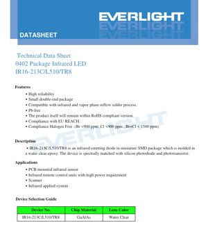
1. Product Overview
This document details the specifications for a high-reliability, miniature surface-mount infrared emitting diode. The device is housed in a compact 0402 package, molded in water-clear epoxy, and is spectrally matched with silicon photodiodes and phototransistors, making it ideal for sensing applications.
1.1 Core Advantages
- High Reliability: Designed for consistent performance in demanding applications.
- Miniature Footprint: The double-ended 0402 package allows for high-density PCB mounting.
- Process Compatibility: Suitable for both infrared and vapor phase reflow soldering processes.
- Environmental Compliance: The product is Pb-free, RoHS compliant, compliant with EU REACH, and meets halogen-free standards (Br <900 ppm, Cl <900 ppm, Br+Cl < 1500 ppm).
1.2 Target Applications
- PCB-mounted infrared sensors
- Infrared remote control units requiring high power output
- Optical scanners
- Various infrared application systems
2. Technical Parameter Deep Dive
2.1 Absolute Maximum Ratings
These ratings define the limits beyond which permanent damage to the device may occur. Operation under these conditions is not guaranteed.
| Parameter | Symbol | Rating | Unit | Notes |
|---|---|---|---|---|
| Continuous Forward Current | IF | 50 | mA | |
| Reverse Voltage | VR | 5 | V | |
| Operating Temperature | Topr | -40 to +100 | °C | |
| Storage Temperature | Tstg | -40 to +100 | °C | |
| Soldering Temperature | Tsol | 260 | °C | Soldering time ≤ 5 seconds. |
| Power Dissipation (Ta=25°C) | Pd | 100 | mW |
2.2 Electro-Optical Characteristics (Ta=25°C)
These are the typical performance parameters measured under standard test conditions (IF=20mA unless noted).
| Parameter | Symbol | Min. | Typ. | Max. | Unit | Condition |
|---|---|---|---|---|---|---|
| Radiant Intensity | Ie | 0.5 | 2.35 | -- | mW/sr | IF=20mA |
| Peak Wavelength | λp | -- | 940 | -- | nm | IF=20mA |
| Spectral Bandwidth (FWHM) | Δλ | -- | 45 | -- | nm | IF=20mA |
| Forward Voltage | VF | -- | 1.5 | 1.9 | V | IF=20mA |
| Reverse Current | IR | -- | -- | 10 | μA | VR=5V |
| Viewing Angle (Half Angle) | 2θ1/2 | -- | 120 | -- | deg | IF=20mA |
3. Performance Curve Analysis
The datasheet provides several characteristic curves essential for design engineers.
3.1 Forward Current vs. Forward Voltage (IV Curve)
The curve shows the exponential relationship between forward current (IF) and forward voltage (VF). At the typical operating point of 20mA, the forward voltage is approximately 1.5V. Designers must use a series current-limiting resistor to prevent exceeding the maximum forward current, as even a small increase in voltage can lead to a large, potentially destructive increase in current.
3.2 Forward Current vs. Ambient Temperature
This derating curve illustrates how the maximum allowable continuous forward current decreases as the ambient temperature increases. The device can handle its full rated current up to approximately 25°C. Beyond this, the maximum current must be reduced linearly to zero at the maximum junction temperature (implied by the 100°C operating limit). This is critical for ensuring long-term reliability in high-temperature environments.
3.3 Spectral Distribution
The spectral output graph confirms the peak emission wavelength at 940nm with a typical spectral bandwidth (Full Width at Half Maximum) of 45nm. This wavelength is near-optimal for silicon-based photodetectors, which have high sensitivity in this region, maximizing the signal-to-noise ratio in sensing applications.
3.4 Relative Radiant Intensity vs. Forward Current
This curve shows that radiant output is nearly linear with forward current in the typical operating range (up to about 40-50mA). This predictable relationship simplifies optical system design.
3.5 Relative Radiant Intensity vs. Angular Displacement
The polar plot depicts the emission pattern, characterized by a wide 120-degree half-angle. This provides a broad, diffuse infrared beam, ideal for applications requiring wide-area coverage or proximity sensing where alignment is not critical.
4. Mechanical and Package Information
4.1 Package Dimensions (0402)
The device conforms to a standard 0402 (Imperial) / 1005 (Metric) footprint. Key dimensions include a body length of approximately 1.0mm, width of 0.5mm, and height of 0.5mm. Terminal dimensions and spacing are provided for PCB land pattern design. All dimensional tolerances are typically ±0.1mm unless otherwise specified.
4.2 Polarity Identification
The package is double-ended. Polarity is typically indicated by a marking on the cathode (-) side or by an internal chip structure visible through the clear lens. The datasheet drawing should be consulted for the exact marking scheme.
5. Soldering and Assembly Guidelines
5.1 Storage and Moisture Sensitivity
The device is moisture-sensitive. Precautions must be taken to prevent popcorning or delamination during reflow:
- Store in original moisture-proof bag at ≤30°C / ≤90% RH.
- Use within one year of shipment.
- After opening the bag, store at ≤30°C / ≤60% RH and use within 168 hours (7 days).
- If the storage time is exceeded or the desiccant indicates moisture, bake at 60±5°C for a minimum of 24 hours before use.
5.2 Reflow Soldering Profile
A recommended Pb-free reflow temperature profile is provided. Key parameters include:
- Preheat and soak zone.
- Peak body temperature not to exceed 260°C.
- Time above liquidus (e.g., 217°C).
- Cooling rate. Reflow soldering should not be performed more than two times.
- Use a soldering iron with a tip temperature <350°C.
- Limit iron power to 25W or less.
- Contact time per terminal should be ≤3 seconds.
- Allow a minimum 2-second interval between soldering each terminal.
- CPN (Customer Part Number)
- P/N (Manufacturer Part Number: IR16-213C/L510/TR8)
- QTY (Quantity)
- CAT (Binning/Rank Code)
- HUE (Peak Wavelength)
- LOT No. (Manufacturing Lot Number)
- Country of Origin
- vs. Larger Packages (e.g., 5mm): Significantly smaller footprint and lower profile, enabling miniaturization. Typically has lower total radiant power output but higher suitability for array or dense placement.
- vs. Other SMD IR LEDs (e.g., 0603): The 0402 package allows for the highest possible component density on a PCB, a critical advantage in space-constrained modern electronics like ultra-compact remote controls or sensors.
- vs. Non-Compliant Devices: Full compliance with RoHS, REACH, and halogen-free standards is a mandatory requirement for most commercial and industrial products today, simplifying the supply chain and end-product certification.
- Increased Power Density: Improving the luminous efficacy (radiant power output per electrical input) of ever-smaller chips.
- Integrated Solutions: Combining the IR emitter, driver, and detector into a single module or package to simplify design and improve performance.
- New Wavelengths: Development of emitters at other IR wavelengths (e.g., 850nm, 1050nm) for specific applications like eye-safe systems or different sensor optimizations.
- Advanced Packaging: Use of materials with better thermal conductivity to manage heat in high-power, miniature devices.
5.3 Hand Soldering and Rework
If hand soldering is necessary:
6. Packaging and Ordering Information
6.1 Tape and Reel Specifications
The device is supplied on embossed carrier tape wound onto reels. A standard reel contains 3000 pieces. Detailed carrier tape dimensions (pocket size, pitch, tape width) and reel specifications are provided for automated pick-and-place machine setup.
6.2 Packing Procedure
Reels are packaged in sealed aluminum moisture barrier bags with desiccant and a humidity indicator card to maintain dry storage conditions.
6.3 Label Information
The package label includes critical information for traceability and verification:
7. Application Design Considerations
7.1 Driving Circuit Design
The most critical design aspect is current limiting. An LED is a current-driven device. A series resistor (Rs) must be calculated based on the supply voltage (Vcc), the desired forward current (IF), and the LED's forward voltage (VF): Rs = (Vcc - VF) / IF. For a 5V supply and 20mA target current: Rs ≈ (5V - 1.5V) / 0.02A = 175Ω. A standard 180Ω resistor would be suitable. Always verify the actual current under worst-case VF (min) to ensure it does not exceed maximum ratings.
7.2 Thermal Management
While the 0402 package has limited thermal mass, attention should be paid to power dissipation, especially in high-current or high-ambient-temperature applications. Ensure the PCB provides adequate copper area around the solder pads to act as a heat sink and follow the current derating guidelines with temperature.
7.3 Optical Design
The wide 120-degree viewing angle makes this LED suitable for applications requiring broad illumination. For longer-range or more directed beams, secondary optics (lenses) may be required. The water-clear lens ensures minimal absorption of the emitted infrared light.
8. Technical Comparison and Differentiation
Compared to other infrared LEDs, this 0402 device offers a key balance:
9. Frequently Asked Questions (FAQ)
9.1 What is the purpose of the 940nm wavelength?
940nm is in the near-infrared spectrum. It is invisible to the human eye but aligns well with the peak sensitivity of inexpensive silicon photodiodes and phototransistors. It also experiences less interference from ambient visible light compared to visible red LEDs, improving signal integrity in sensing applications.
9.2 Why is a current-limiting resistor absolutely necessary?
The I-V characteristic of an LED is exponential. Beyond the knee voltage, a tiny increase in voltage causes a very large increase in current. Without a series resistor to control the current, connecting the LED directly to a voltage source (even a small battery) will almost certainly drive it beyond its maximum current rating, causing instantaneous overheating and failure.
9.3 Can I use this for data transmission (like IR remote controls)?
Yes, this is a primary application. Its fast switching speed (implied by the GaAlAs material) and compatibility with high-current pulses make it suitable for modulated data transmission in remote controls, IR data association (IrDA) systems, and optical isolation.
9.4 How do I interpret the \"Radiant Intensity\" specification?
Radiant Intensity (Ie) of 2.35 mW/sr (typical) means the LED emits 2.35 milliwatts of optical power per steradian (a unit of solid angle) along its central axis. This is a measure of how \"bright\" the IR source is in its main direction. The total radiant flux (power in mW) can be estimated by multiplying intensity by the solid angle of the beam.
10. Design and Use Case Example
10.1 Simple Proximity Sensor
A common application is a reflectance-based proximity sensor. The IR LED is placed adjacent to a phototransistor on a PCB. A microcontroller drives the LED with a pulsed current (e.g., 20mA pulses). The phototransistor detects IR light reflected off an object. The strength of the detected signal correlates with the object's distance and reflectivity. The wide viewing angle of this LED ensures good coverage for detecting objects that may not be perfectly aligned.
11. Operating Principle
An Infrared Light Emitting Diode (IR LED) is a semiconductor p-n junction diode. When forward biased, electrons from the n-region recombine with holes from the p-region in the active region (GaAlAs chip). This recombination process releases energy in the form of photons (light). The specific wavelength of the emitted photons (940nm in this case) is determined by the bandgap energy of the semiconductor material used. The water-clear epoxy package encapsulates and protects the chip while allowing the infrared light to pass through with minimal loss.
12. Industry Trends
The trend in optoelectronics, as in all electronics, is toward miniaturization, higher integration, and improved efficiency. The 0402 package represents the ongoing push for smaller passive and active components. Future developments may include:
LED Specification Terminology
Complete explanation of LED technical terms
Photoelectric Performance
| Term | Unit/Representation | Simple Explanation | Why Important |
|---|---|---|---|
| Luminous Efficacy | lm/W (lumens per watt) | Light output per watt of electricity, higher means more energy efficient. | Directly determines energy efficiency grade and electricity cost. |
| Luminous Flux | lm (lumens) | Total light emitted by source, commonly called "brightness". | Determines if the light is bright enough. |
| Viewing Angle | ° (degrees), e.g., 120° | Angle where light intensity drops to half, determines beam width. | Affects illumination range and uniformity. |
| CCT (Color Temperature) | K (Kelvin), e.g., 2700K/6500K | Warmth/coolness of light, lower values yellowish/warm, higher whitish/cool. | Determines lighting atmosphere and suitable scenarios. |
| CRI / Ra | Unitless, 0–100 | Ability to render object colors accurately, Ra≥80 is good. | Affects color authenticity, used in high-demand places like malls, museums. |
| SDCM | MacAdam ellipse steps, e.g., "5-step" | Color consistency metric, smaller steps mean more consistent color. | Ensures uniform color across same batch of LEDs. |
| Dominant Wavelength | nm (nanometers), e.g., 620nm (red) | Wavelength corresponding to color of colored LEDs. | Determines hue of red, yellow, green monochrome LEDs. |
| Spectral Distribution | Wavelength vs intensity curve | Shows intensity distribution across wavelengths. | Affects color rendering and quality. |
Electrical Parameters
| Term | Symbol | Simple Explanation | Design Considerations |
|---|---|---|---|
| Forward Voltage | Vf | Minimum voltage to turn on LED, like "starting threshold". | Driver voltage must be ≥Vf, voltages add up for series LEDs. |
| Forward Current | If | Current value for normal LED operation. | Usually constant current drive, current determines brightness & lifespan. |
| Max Pulse Current | Ifp | Peak current tolerable for short periods, used for dimming or flashing. | Pulse width & duty cycle must be strictly controlled to avoid damage. |
| Reverse Voltage | Vr | Max reverse voltage LED can withstand, beyond may cause breakdown. | Circuit must prevent reverse connection or voltage spikes. |
| Thermal Resistance | Rth (°C/W) | Resistance to heat transfer from chip to solder, lower is better. | High thermal resistance requires stronger heat dissipation. |
| ESD Immunity | V (HBM), e.g., 1000V | Ability to withstand electrostatic discharge, higher means less vulnerable. | Anti-static measures needed in production, especially for sensitive LEDs. |
Thermal Management & Reliability
| Term | Key Metric | Simple Explanation | Impact |
|---|---|---|---|
| Junction Temperature | Tj (°C) | Actual operating temperature inside LED chip. | Every 10°C reduction may double lifespan; too high causes light decay, color shift. |
| Lumen Depreciation | L70 / L80 (hours) | Time for brightness to drop to 70% or 80% of initial. | Directly defines LED "service life". |
| Lumen Maintenance | % (e.g., 70%) | Percentage of brightness retained after time. | Indicates brightness retention over long-term use. |
| Color Shift | Δu′v′ or MacAdam ellipse | Degree of color change during use. | Affects color consistency in lighting scenes. |
| Thermal Aging | Material degradation | Deterioration due to long-term high temperature. | May cause brightness drop, color change, or open-circuit failure. |
Packaging & Materials
| Term | Common Types | Simple Explanation | Features & Applications |
|---|---|---|---|
| Package Type | EMC, PPA, Ceramic | Housing material protecting chip, providing optical/thermal interface. | EMC: good heat resistance, low cost; Ceramic: better heat dissipation, longer life. |
| Chip Structure | Front, Flip Chip | Chip electrode arrangement. | Flip chip: better heat dissipation, higher efficacy, for high-power. |
| Phosphor Coating | YAG, Silicate, Nitride | Covers blue chip, converts some to yellow/red, mixes to white. | Different phosphors affect efficacy, CCT, and CRI. |
| Lens/Optics | Flat, Microlens, TIR | Optical structure on surface controlling light distribution. | Determines viewing angle and light distribution curve. |
Quality Control & Binning
| Term | Binning Content | Simple Explanation | Purpose |
|---|---|---|---|
| Luminous Flux Bin | Code e.g., 2G, 2H | Grouped by brightness, each group has min/max lumen values. | Ensures uniform brightness in same batch. |
| Voltage Bin | Code e.g., 6W, 6X | Grouped by forward voltage range. | Facilitates driver matching, improves system efficiency. |
| Color Bin | 5-step MacAdam ellipse | Grouped by color coordinates, ensuring tight range. | Guarantees color consistency, avoids uneven color within fixture. |
| CCT Bin | 2700K, 3000K etc. | Grouped by CCT, each has corresponding coordinate range. | Meets different scene CCT requirements. |
Testing & Certification
| Term | Standard/Test | Simple Explanation | Significance |
|---|---|---|---|
| LM-80 | Lumen maintenance test | Long-term lighting at constant temperature, recording brightness decay. | Used to estimate LED life (with TM-21). |
| TM-21 | Life estimation standard | Estimates life under actual conditions based on LM-80 data. | Provides scientific life prediction. |
| IESNA | Illuminating Engineering Society | Covers optical, electrical, thermal test methods. | Industry-recognized test basis. |
| RoHS / REACH | Environmental certification | Ensures no harmful substances (lead, mercury). | Market access requirement internationally. |
| ENERGY STAR / DLC | Energy efficiency certification | Energy efficiency and performance certification for lighting. | Used in government procurement, subsidy programs, enhances competitiveness. |