Table of Contents
- 1. Product Overview
- 1.1 Core Advantages and Target Market
- 2. In-Depth Technical Parameter Analysis
- 2.1 Absolute Maximum Ratings
- 2.2 Electro-Optical Characteristics (Ta = 25°C)
- 3. Binning System Explanation
- 3.1 Radiant Intensity Binning
- 4. Performance Curve Analysis
- 4.1 Forward Current vs. Ambient Temperature
- 4.2 Spectral Distribution
- 3.3 Peak Emission Wavelength vs. Ambient Temperature
- 4.4 Forward Current vs. Forward Voltage (I-V Curve)
- 4.5 Relative Radiant Intensity vs. Angular Displacement
- 5. Mechanical and Package Information
- 5.1 Package Dimensions
- 5.2 Polarity Identification
- 6. Soldering and Assembly Guidelines
- 6.1 Storage and Moisture Sensitivity
- 6.2 Reflow Soldering Profile
- 6.3 Hand Soldering and Rework
- 7. Packaging and Ordering Information
- 7.1 Tape and Reel Specifications
- 7.2 Packing Procedure
- 8. Application Design Recommendations
- 8.1 Current Limiting is Mandatory
- 8.2 Thermal Management
- 8.3 Optical Design Considerations
- 9. Technical Comparison and Differentiation
- 10. Frequently Asked Questions (FAQ)
- 10.1 What is the purpose of the binning codes (E, F, G)?
- 10.2 Can I drive this LED directly from a 3.3V or 5V microcontroller pin?
- 10.3 Why is the 940nm wavelength significant?
- 10.4 How many times can I reflow solder this component?
- 11. Design and Usage Case Studies
- 11.1 Simple Proximity Sensor
- 11.2 Infrared Remote Control Transmitter
- 12. Operating Principle
- 13. Technology Trends
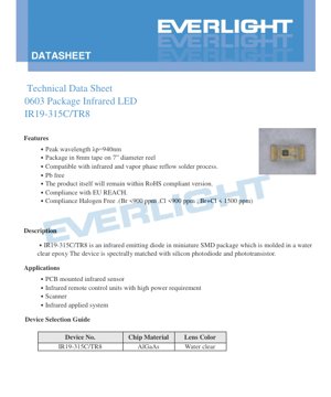
1. Product Overview
The IR19-315C/TR8 is a miniature surface-mount infrared light-emitting diode (LED) housed in a standard 0603 package. This device is engineered to emit light at a peak wavelength of 940 nanometers (nm), which is optimally matched to the spectral sensitivity of silicon photodiodes and phototransistors. Its primary function is to serve as an efficient infrared source in various sensing and communication systems.
1.1 Core Advantages and Target Market
This component offers several key advantages for modern electronic design. Its miniature SMD footprint allows for high-density PCB layouts, essential for compact consumer electronics and IoT devices. The device is constructed using AlGaAs (Aluminum Gallium Arsenide) chip material, which provides reliable performance for infrared emission. It is encapsulated in a water-clear epoxy lens, ensuring minimal absorption of the emitted IR light. The product is fully compliant with RoHS (Restriction of Hazardous Substances), EU REACH regulations, and is manufactured as halogen-free, meeting stringent environmental and safety standards. The primary target applications include infrared remote control units requiring consistent output, PCB-mounted proximity or object detection sensors, barcode scanners, and various other infrared-based systems.
2. In-Depth Technical Parameter Analysis
A thorough understanding of the device's limits and operating characteristics is crucial for reliable circuit design and ensuring long-term performance.
2.1 Absolute Maximum Ratings
These ratings define the stress limits beyond which permanent damage to the device may occur. Operation under or at these limits is not guaranteed.
- Continuous Forward Current (IF): 65 mA. This is the maximum DC current that can be continuously applied to the LED.
- Reverse Voltage (VR): 5 V. Exceeding this voltage in reverse bias can cause junction breakdown.
- Operating Temperature (Topr): -25°C to +85°C. The ambient temperature range for normal operation.
- Storage Temperature (Tstg): -40°C to +100°C. The temperature range for non-operational storage.
- Power Dissipation (Pd): 130 mW at or below 25°C free air temperature. The maximum power the package can dissipate as heat.
- Soldering Temperature (Tsol): 260°C for a duration not exceeding 5 seconds, applicable for reflow processes.
2.2 Electro-Optical Characteristics (Ta = 25°C)
These parameters define the device's performance under typical operating conditions. All values are specified at an ambient temperature of 25°C.
- Radiant Intensity (Ie): This is the optical power emitted per unit solid angle, measured in milliwatts per steradian (mW/sr). At a forward current (IF) of 20 mA, the typical value is 0.6 mW/sr. Under pulsed operation (IF=100mA, pulse width ≤100μs, duty cycle ≤1%), the radiant intensity can reach up to 4.0 mW/sr.
- Peak Wavelength (λp): 940 nm. This is the wavelength at which the optical output power is maximum.
- Spectral Bandwidth (Δλ): Approximately 45 nm. This indicates the range of wavelengths emitted, typically measured at half the maximum intensity (Full Width at Half Maximum - FWHM).
- Forward Voltage (VF): The voltage drop across the LED when current is flowing. At IF=20mA, the typical VF is 1.2V, with a maximum of 1.5V. This increases to 1.4V (typical) and 1.8V (max) at IF=100mA under pulsed conditions.
- Reverse Current (IR): Maximum of 10 μA when a reverse voltage of 5V is applied.
- Viewing Angle (2θ1/2): 140 degrees. This is the full angle where the radiant intensity drops to half of its value at 0 degrees (on-axis). A wide viewing angle is beneficial for applications requiring broad area coverage.
3. Binning System Explanation
The IR19-315C/TR8 utilizes a binning system to categorize devices based on their radiant intensity output. This allows designers to select components that meet specific brightness requirements for their application.
3.1 Radiant Intensity Binning
Devices are sorted into bins (E, F, G) according to their measured radiant intensity at a test condition of IF = 20 mA.
- Bin E: Radiant intensity ranges from a minimum of 0.2 mW/sr to a maximum of 1.0 mW/sr.
- Bin F: Radiant intensity ranges from a minimum of 0.5 mW/sr to a maximum of 1.5 mW/sr.
- Bin G: Radiant intensity ranges from a minimum of 1.0 mW/sr to a maximum of 2.5 mW/sr.
This grading ensures consistency within a production batch and allows for predictable optical performance in the final product.
4. Performance Curve Analysis
The datasheet provides several characteristic curves that illustrate the device's behavior under varying conditions. These are essential for advanced design and understanding non-linear effects.
4.1 Forward Current vs. Ambient Temperature
This curve shows the derating of the maximum allowable forward current as the ambient temperature increases. The LED's power dissipation capability decreases with rising temperature to prevent overheating. Designers must consult this graph when operating the device in elevated temperature environments to ensure the driving current does not exceed the safe operating area.
4.2 Spectral Distribution
The spectral distribution plot illustrates the relative optical power output across different wavelengths. It confirms the peak at 940nm and the approximately 45nm spectral bandwidth. This is critical for ensuring compatibility with the receiving sensor's spectral response.
3.3 Peak Emission Wavelength vs. Ambient Temperature
This graph depicts how the peak wavelength (λp) shifts with changes in junction temperature. Typically, the wavelength increases slightly with temperature (a positive coefficient). This shift must be considered in precision sensing applications where the receiver's filter or sensitivity is narrowly tuned.
4.4 Forward Current vs. Forward Voltage (I-V Curve)
The I-V curve is fundamental for circuit design. It shows the exponential relationship between current and voltage. The "knee" voltage is around 1.2V. This curve is used to calculate the necessary series resistor value to limit the current to a desired level when driven from a voltage source, as emphasized in the precautions.
4.5 Relative Radiant Intensity vs. Angular Displacement
This polar plot visually represents the viewing angle. It shows how the intensity diminishes as the observation angle moves away from the central axis (0°), dropping to 50% at ±70° (hence the 140° total viewing angle). This information is vital for designing the optical path and alignment in a system.
5. Mechanical and Package Information
5.1 Package Dimensions
The device conforms to the standard 0603 (1608 metric) SMD package footprint. Key dimensions include a body length of 1.6 mm, a width of 0.8 mm, and a height of 0.6 mm. The land pattern (recommended PCB pad layout) and terminal dimensions are provided to ensure proper soldering and mechanical stability. All dimensional tolerances are typically ±0.1 mm unless otherwise specified.
5.2 Polarity Identification
The cathode is typically marked on the device body. The datasheet diagram indicates the cathode side, which must be correctly oriented on the PCB according to the recommended footprint. Incorrect polarity will prevent the device from emitting light and applying reverse bias.
6. Soldering and Assembly Guidelines
Proper handling and soldering are critical to maintaining device reliability and performance.
6.1 Storage and Moisture Sensitivity
The LEDs are packaged in a moisture-proof bag with desiccant. Key precautions include:
- Do not open the bag until ready for use.
- Store unopened bags at ≤30°C and ≤90% RH.
- Use within one year of shipment.
- After opening, store at ≤30°C and ≤60% RH and use within 168 hours (7 days).
- If the storage time is exceeded or the desiccant indicates moisture, a baking treatment at 60 ±5°C for a minimum of 24 hours is required before soldering.
6.2 Reflow Soldering Profile
The device is compatible with infrared and vapor phase reflow processes. A lead-free soldering temperature profile is recommended, with a peak temperature of 260°C for no more than 5 seconds. Reflow soldering should not be performed more than two times. Stress on the LED body during heating and warping of the PCB after soldering must be avoided.
6.3 Hand Soldering and Rework
If hand soldering is necessary, use a soldering iron with a tip temperature below 350°C, apply heat to each terminal for no more than 3 seconds, and use an iron with a power rating of 25W or less. Allow a cooling interval of at least 2 seconds between terminals. Rework is discouraged, but if unavoidable, a double-head soldering iron should be used to simultaneously heat both terminals to prevent mechanical stress on the solder joints. The effect of rework on device characteristics should be verified beforehand.
7. Packaging and Ordering Information
7.1 Tape and Reel Specifications
The components are supplied on 8mm wide embossed carrier tape wound on a standard 7-inch diameter reel. Each reel contains 4000 pieces (4k pcs/reel). Detailed carrier tape dimensions, including pocket size, pitch, and sprocket hole specifications, are provided to ensure compatibility with automated pick-and-place equipment.
7.2 Packing Procedure
The reels are sealed inside an aluminum moisture-proof bag along with desiccant. Labels on the bag provide key information such as the part number (P/N), customer part number (CPN), quantity (QTY), bin rank (CAT), peak wavelength (HUE), lot number (LOT No.), and country of manufacture.
8. Application Design Recommendations
8.1 Current Limiting is Mandatory
The most critical design rule is the mandatory use of a series current-limiting resistor. The forward voltage of an LED has a negative temperature coefficient and can vary slightly between units. A small increase in voltage can cause a large, potentially destructive increase in current. The resistor value (R) can be calculated using Ohm's Law: R = (Vsupply - VF) / IF, where VF is the forward voltage at the desired current IF.
8.2 Thermal Management
While the 0603 package has limited thermal mass, attention should be paid to the power dissipation, especially when driving at higher currents or in high ambient temperatures. The derating curve must be followed. Ensuring adequate copper area connected to the thermal pads (if any) or the device terminals can help dissipate heat into the PCB.
8.3 Optical Design Considerations
The 140° wide viewing angle makes this LED suitable for applications requiring broad illumination, such as proximity sensors. For longer-range or directed beams, secondary optics (lenses) may be required. The 940nm wavelength is invisible to the human eye, making it ideal for discreet operation, but it is important to note that some consumer-grade digital camera sensors can detect it, which may appear as a purple glow.
9. Technical Comparison and Differentiation
The IR19-315C/TR8 differentiates itself within the 0603 infrared LED category through its specific combination of AlGaAs material and 940nm peak wavelength. AlGaAs LEDs generally offer good efficiency and reliability at this wavelength. Compared to GaAs-based LEDs, AlGaAs devices can have slightly different forward voltage and temperature characteristics. The wide 140° viewing angle is a notable feature compared to some competitors offering narrower beams, making it more versatile for area-sensing applications.
10. Frequently Asked Questions (FAQ)
10.1 What is the purpose of the binning codes (E, F, G)?
The binning codes categorize the LEDs based on their measured radiant intensity output. This allows designers to select a consistent brightness level for their product. For example, an application requiring higher optical output would specify Bin G components.
10.2 Can I drive this LED directly from a 3.3V or 5V microcontroller pin?
No, you must not connect it directly. The LED's low forward voltage (typically 1.2V) means that connecting it directly to a 3.3V or 5V source without a current-limiting resistor would cause excessive current to flow, instantly destroying the device. A series resistor is always required.
10.3 Why is the 940nm wavelength significant?
940nm is a very common wavelength for infrared systems because it falls within a region where silicon photodetectors (photodiodes, phototransistors) have high sensitivity. It is also less visible to ambient light noise compared to shorter IR wavelengths like 850nm, and it is invisible to the human eye, which is desirable for consumer electronics.
10.4 How many times can I reflow solder this component?
The datasheet specifies that reflow soldering should not be performed more than two times. Each reflow cycle subjects the component to thermal stress, which can potentially degrade the internal wire bonds or the epoxy encapsulation.
11. Design and Usage Case Studies
11.1 Simple Proximity Sensor
A common application is a basic reflective object sensor. The IR19-315C/TR8 is placed adjacent to a silicon phototransistor on a PCB. The LED is driven with a pulsed current (e.g., 20mA, 1kHz, 50% duty cycle) through a resistor. When an object comes near, it reflects the IR light onto the phototransistor, which conducts and produces a signal. The pulsed operation helps distinguish the signal from ambient IR light. The wide viewing angle of the LED ensures good coverage of the detection area.
11.2 Infrared Remote Control Transmitter
For remote controls requiring longer range or higher output, the LED can be driven in a pulsed mode at higher currents, such as 100mA with a very low duty cycle (e.g., ≤1%). This takes advantage of the higher pulsed radiant intensity (up to 4.0 mW/sr) while keeping the average power and heat dissipation within limits. The signal is typically modulated at a carrier frequency (e.g., 38kHz) to allow the receiver to filter out noise.
12. Operating Principle
The IR19-315C/TR8 is a semiconductor p-n junction diode. When a forward voltage exceeding its bandgap energy is applied, electrons from the n-type AlGaAs material recombine with holes from the p-type material in the active region. This recombination process releases energy in the form of photons (light). The specific composition of the AlGaAs semiconductor determines the bandgap energy, which in turn dictates the wavelength of the emitted photons—in this case, approximately 940nm, which is in the near-infrared spectrum.
13. Technology Trends
Infrared LED technology continues to evolve alongside visible LED technology. Trends include the development of devices with higher wall-plug efficiency (more light output per electrical watt input), which reduces power consumption and heat generation. There is also ongoing work to improve the high-temperature performance and reliability of SMD packages. Furthermore, the integration of IR LEDs with drivers and sensors into compact modules is a growing trend, simplifying system design for applications like gesture recognition and 3D sensing (e.g., time-of-flight). The 940nm wavelength remains a dominant standard due to its optimal match with silicon detectors and its low visibility.
LED Specification Terminology
Complete explanation of LED technical terms
Photoelectric Performance
| Term | Unit/Representation | Simple Explanation | Why Important |
|---|---|---|---|
| Luminous Efficacy | lm/W (lumens per watt) | Light output per watt of electricity, higher means more energy efficient. | Directly determines energy efficiency grade and electricity cost. |
| Luminous Flux | lm (lumens) | Total light emitted by source, commonly called "brightness". | Determines if the light is bright enough. |
| Viewing Angle | ° (degrees), e.g., 120° | Angle where light intensity drops to half, determines beam width. | Affects illumination range and uniformity. |
| CCT (Color Temperature) | K (Kelvin), e.g., 2700K/6500K | Warmth/coolness of light, lower values yellowish/warm, higher whitish/cool. | Determines lighting atmosphere and suitable scenarios. |
| CRI / Ra | Unitless, 0–100 | Ability to render object colors accurately, Ra≥80 is good. | Affects color authenticity, used in high-demand places like malls, museums. |
| SDCM | MacAdam ellipse steps, e.g., "5-step" | Color consistency metric, smaller steps mean more consistent color. | Ensures uniform color across same batch of LEDs. |
| Dominant Wavelength | nm (nanometers), e.g., 620nm (red) | Wavelength corresponding to color of colored LEDs. | Determines hue of red, yellow, green monochrome LEDs. |
| Spectral Distribution | Wavelength vs intensity curve | Shows intensity distribution across wavelengths. | Affects color rendering and quality. |
Electrical Parameters
| Term | Symbol | Simple Explanation | Design Considerations |
|---|---|---|---|
| Forward Voltage | Vf | Minimum voltage to turn on LED, like "starting threshold". | Driver voltage must be ≥Vf, voltages add up for series LEDs. |
| Forward Current | If | Current value for normal LED operation. | Usually constant current drive, current determines brightness & lifespan. |
| Max Pulse Current | Ifp | Peak current tolerable for short periods, used for dimming or flashing. | Pulse width & duty cycle must be strictly controlled to avoid damage. |
| Reverse Voltage | Vr | Max reverse voltage LED can withstand, beyond may cause breakdown. | Circuit must prevent reverse connection or voltage spikes. |
| Thermal Resistance | Rth (°C/W) | Resistance to heat transfer from chip to solder, lower is better. | High thermal resistance requires stronger heat dissipation. |
| ESD Immunity | V (HBM), e.g., 1000V | Ability to withstand electrostatic discharge, higher means less vulnerable. | Anti-static measures needed in production, especially for sensitive LEDs. |
Thermal Management & Reliability
| Term | Key Metric | Simple Explanation | Impact |
|---|---|---|---|
| Junction Temperature | Tj (°C) | Actual operating temperature inside LED chip. | Every 10°C reduction may double lifespan; too high causes light decay, color shift. |
| Lumen Depreciation | L70 / L80 (hours) | Time for brightness to drop to 70% or 80% of initial. | Directly defines LED "service life". |
| Lumen Maintenance | % (e.g., 70%) | Percentage of brightness retained after time. | Indicates brightness retention over long-term use. |
| Color Shift | Δu′v′ or MacAdam ellipse | Degree of color change during use. | Affects color consistency in lighting scenes. |
| Thermal Aging | Material degradation | Deterioration due to long-term high temperature. | May cause brightness drop, color change, or open-circuit failure. |
Packaging & Materials
| Term | Common Types | Simple Explanation | Features & Applications |
|---|---|---|---|
| Package Type | EMC, PPA, Ceramic | Housing material protecting chip, providing optical/thermal interface. | EMC: good heat resistance, low cost; Ceramic: better heat dissipation, longer life. |
| Chip Structure | Front, Flip Chip | Chip electrode arrangement. | Flip chip: better heat dissipation, higher efficacy, for high-power. |
| Phosphor Coating | YAG, Silicate, Nitride | Covers blue chip, converts some to yellow/red, mixes to white. | Different phosphors affect efficacy, CCT, and CRI. |
| Lens/Optics | Flat, Microlens, TIR | Optical structure on surface controlling light distribution. | Determines viewing angle and light distribution curve. |
Quality Control & Binning
| Term | Binning Content | Simple Explanation | Purpose |
|---|---|---|---|
| Luminous Flux Bin | Code e.g., 2G, 2H | Grouped by brightness, each group has min/max lumen values. | Ensures uniform brightness in same batch. |
| Voltage Bin | Code e.g., 6W, 6X | Grouped by forward voltage range. | Facilitates driver matching, improves system efficiency. |
| Color Bin | 5-step MacAdam ellipse | Grouped by color coordinates, ensuring tight range. | Guarantees color consistency, avoids uneven color within fixture. |
| CCT Bin | 2700K, 3000K etc. | Grouped by CCT, each has corresponding coordinate range. | Meets different scene CCT requirements. |
Testing & Certification
| Term | Standard/Test | Simple Explanation | Significance |
|---|---|---|---|
| LM-80 | Lumen maintenance test | Long-term lighting at constant temperature, recording brightness decay. | Used to estimate LED life (with TM-21). |
| TM-21 | Life estimation standard | Estimates life under actual conditions based on LM-80 data. | Provides scientific life prediction. |
| IESNA | Illuminating Engineering Society | Covers optical, electrical, thermal test methods. | Industry-recognized test basis. |
| RoHS / REACH | Environmental certification | Ensures no harmful substances (lead, mercury). | Market access requirement internationally. |
| ENERGY STAR / DLC | Energy efficiency certification | Energy efficiency and performance certification for lighting. | Used in government procurement, subsidy programs, enhances competitiveness. |