Table of Contents
- 1. Product Overview
- 2. Technical Parameter Deep Dive
- 2.1 Absolute Maximum Ratings
- 2.2 Electro-Optical Characteristics
- 3. Performance Curve Analysis
- 3.1 IR Emitter Characteristics
- 3.2 Phototransistor Characteristics
- 4. Mechanical and Package Information
- 4.1 Package Dimensions
- 4.2 Polarity Identification
- 5. Soldering and Assembly Guidelines
- 5.1 Lead Forming
- 5.2 Soldering Process
- 5.3 Cleaning and Storage
- 6. Packaging and Ordering Information
- 7. Application Suggestions
- 7.1 Typical Application Scenarios
- 7.2 Design Considerations
- 8. Technical Comparison and Differentiation
- 9. Frequently Asked Questions (FAQs)
- 9.1 What is the typical sensing distance or gap?
- 9.2 Can I drive the IRED with a voltage source directly?
- 9.3 How do I interface the phototransistor output to a microcontroller?
- 9.4 Why is the soldering distance (3mm) so critical?
- 10. Practical Design Case
- 11. Operating Principle
- 12. Technology Trends
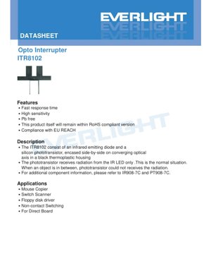
1. Product Overview
The ITR8102 is a compact opto interrupter module designed for non-contact sensing applications. It integrates an infrared emitting diode (IRED) and a silicon phototransistor aligned on converging optical axes within a black thermoplastic housing. This configuration allows the phototransistor to receive radiation from the IRED under normal conditions. When an opaque object interrupts the light path between the emitter and detector, the phototransistor ceases to conduct, enabling object detection or position sensing.
Key features include a fast response time, high sensitivity, and compliance with environmental standards such as RoHS and EU REACH. The device is constructed using lead-free materials.
2. Technical Parameter Deep Dive
2.1 Absolute Maximum Ratings
These ratings define the limits beyond which permanent damage to the device may occur. Operation under these conditions is not guaranteed.
- Input Power Dissipation (Pd): 75 mW at or below 25°C free air temperature.
- Input Reverse Voltage (VR): 5 V maximum.
- Input Forward Current (IF): 50 mA maximum.
- Output Collector Power Dissipation (Pc): 75 mW.
- Output Collector Current (IC): 20 mA maximum.
- Collector-Emitter Voltage (BVCEO): 30 V maximum.
- Operating Temperature (Topr): -25°C to +85°C.
- Storage Temperature (Tstg): -40°C to +85°C.
- Lead Soldering Temperature (Tsol): 260°C for less than 5 seconds, measured 3mm from the package.
2.2 Electro-Optical Characteristics
These parameters are measured at Ta=25°C and define the typical operating performance.
- Forward Voltage (VF): Typically 1.25V, with a maximum of 1.60V at IF=20mA.
- Reverse Current (IR): Maximum 10 μA at VR=5V.
- Peak Wavelength (λP): 940 nm at IF=20mA.
- Dark Current (ICEO): Maximum 100 nA at VCE=20V with zero irradiance (Ee=0 mW/cm²).
- Collector-Emitter Saturation Voltage (VCE(sat)): Maximum 0.4V at IC=0.9mA and IF=20mA.
- Collector Current (IC(ON)): Minimum 0.9mA, typical values higher, up to a maximum of 15mA at VCE=5V and IF=20mA.
- Rise/Fall Time (tr, tf): Typically 15 μsec each under specified test conditions (VCE=5V, IC=1mA, RL=1kΩ).
3. Performance Curve Analysis
3.1 IR Emitter Characteristics
The datasheet provides typical curves for the infrared emitter component. The Forward Current vs. Forward Voltage curve shows the non-linear relationship, essential for designing the current-limiting driver circuit. The Forward Current vs. Ambient Temperature curve illustrates the necessary de-rating of the maximum allowable forward current as ambient temperature increases to prevent overheating. The Spectral Distribution curve confirms the peak emission at 940nm, which is optimal for matching the phototransistor's sensitivity and minimizing interference from ambient visible light.
3.2 Phototransistor Characteristics
The key curve for the phototransistor is the Spectral Sensitivity plot. It shows the detector's responsivity across different wavelengths, peaking in the near-infrared region around 940nm. This precise spectral matching with the IR emitter's output ensures high sensitivity and signal-to-noise ratio in the sensing system.
4. Mechanical and Package Information
4.1 Package Dimensions
The ITR8102 is housed in a standard 4-pin side-looking package. Critical dimensions include an overall body size of approximately 4.8mm in length, 4.8mm in height, and 3.2mm in width (excluding leads). The lead spacing is 2.54mm (0.1 inches). All dimensions are in millimeters with a general tolerance of ±0.3mm unless otherwise specified. The leads emerge from the bottom of the black plastic housing, which acts as an optical barrier to prevent crosstalk between the emitter and detector.
4.2 Polarity Identification
The component uses a standard pinout configuration. When viewing the device from the front (the side with the lens openings), the pins are typically arranged as follows from left to right: Anode of the IRED, Cathode of the IRED, Emitter of the phototransistor, Collector of the phototransistor. It is crucial to consult the package diagram for definitive identification to ensure correct circuit connection.
5. Soldering and Assembly Guidelines
5.1 Lead Forming
Leads must be formed before soldering. Bending should occur at a distance greater than 3mm from the bottom of the epoxy package body to avoid stress-induced cracks or performance degradation. The lead frame must be securely held during bending to prevent stress on the epoxy bulb. Cutting of leads should be performed at room temperature.
5.2 Soldering Process
Recommended soldering conditions are critical for reliability.
- Hand Soldering: Iron tip temperature maximum 300°C (for a 30W iron), soldering time maximum 3 seconds per lead.
- Wave/DIP Soldering: Preheat temperature maximum 100°C for up to 60 seconds. Solder bath temperature maximum 260°C for a maximum dwell time of 5 seconds.
- Critical Distance: The solder joint must be at least 3mm away from the epoxy bulb to prevent thermal damage.
- Process Limit: Dip or hand soldering should not be performed more than once.
A recommended soldering temperature profile is provided, emphasizing a controlled ramp-up, a peak temperature plateau, and a controlled cooldown phase to minimize thermal shock.
5.3 Cleaning and Storage
Ultrasonic cleaning is prohibited as it can damage the internal components or the epoxy seal. For storage, devices should be kept at 10-30°C and ≤70% RH for up to 3 months after shipment. For longer storage (up to one year), a nitrogen atmosphere at 10-25°C and 20-60% RH is recommended. After opening the moisture barrier bag, devices should be used within 24 hours or resealed promptly.
6. Packaging and Ordering Information
The standard packing specification is 100 pieces per tube, 20 tubes per box, and 4 boxes per carton, totaling 8000 pieces per carton. The label on the packaging includes fields for Customer Part Number (CPN), Manufacturer Part Number (P/N), Packing Quantity (QTY), and Lot Number (LOT No.) for traceability.
7. Application Suggestions
7.1 Typical Application Scenarios
The ITR8102 is suitable for various non-contact sensing and switching applications, including but not limited to:
- Position Sensing in Printers/Scanners/Copiers: Detecting paper presence, tray position, or carriage home position.
- Rotary Encoding: Used in conjunction with a slotted wheel to measure speed or position in motors, fans, or floppy disk drives.
- Object Detection: Detecting the presence or absence of an object in vending machines, industrial automation, or security systems.
- Non-contact Switching: Implementing touchless switches in consumer electronics or appliances.
7.2 Design Considerations
- Current Limiting Resistor: An external resistor must be connected in series with the IRED anode to limit the forward current (IF) to the desired value (e.g., 20mA for typical operation), calculated based on the supply voltage and the IRED's forward voltage (VF).
- Phototransistor Biasing: A load resistor (RL) is connected between the phototransistor's collector and the positive supply. The value of RL determines the output voltage swing and switching speed. A typical value is 1kΩ.
- Ambient Light Immunity: The black housing and the 940nm matched wavelength pair provide good rejection of ambient visible light. For high ambient IR environments, modulation/demodulation techniques may be necessary.
- Aperture and Gap Design: The sensing distance and resolution depend on the size and alignment of the object interrupting the beam. The converging optical axis defines a specific sensing gap.
- Heat Management: The forward current must be de-rated at higher ambient temperatures as per the derating curve to ensure the input power dissipation (Pd) does not exceed safe limits.
8. Technical Comparison and Differentiation
The ITR8102 offers a balanced set of specifications for general-purpose opto-interruption. Its key differentiators include a relatively fast 15μs response time suitable for medium-speed sensing, a high minimum collector current (0.9mA) ensuring a strong output signal, and a compact, industry-standard package. Compared to reflective sensors, interrupter modules like the ITR8102 provide higher reliability and consistency as they are immune to variations in the reflectivity of the target object. The side-by-side configuration with a physical gap is ideal for detecting objects that pass through a specific plane.
9. Frequently Asked Questions (FAQs)
9.1 What is the typical sensing distance or gap?
The sensing gap is defined by the mechanical separation between the emitter and detector lenses inside the package. For the ITR8102, this is a fixed, internal gap. The device detects any opaque object that is inserted into this gap and interrupts the infrared beam. The effective "sensing distance" is essentially zero, as the object must physically enter the slot.
9.2 Can I drive the IRED with a voltage source directly?
No. The IRED is a diode with a dynamic resistance and a forward voltage drop. Connecting it directly to a voltage source exceeding its VF will cause excessive current flow, potentially destroying the device. A series current-limiting resistor is mandatory.
9.3 How do I interface the phototransistor output to a microcontroller?
The phototransistor acts as a light-dependent switch. With the load resistor (RL) connected to VCC, the collector output will be pulled low (near VCE(sat)) when the beam is unblocked (ON state). When the beam is blocked, the transistor turns off, and the collector output goes high (to VCC). This digital signal can be directly read by a microcontroller's digital input pin. For analog sensing of light intensity, the voltage across RL can be measured with an ADC, though linearity may be limited.
9.4 Why is the soldering distance (3mm) so critical?
The epoxy package encapsulating the semiconductor chips is sensitive to extreme thermal stress. Soldering too close to the body can transfer excessive heat, potentially cracking the epoxy, damaging the wire bonds inside, or altering the optical properties of the lens, leading to immediate failure or reduced long-term reliability.
10. Practical Design Case
Case: Paper-Out Sensor in a Desktop Printer
In this application, the ITR8102 is mounted on the printer's main board, positioned so its sensing gap aligns with a path through which the paper stack passes. A mechanical lever or flag attached to the paper tray moves into the sensor's gap when the paper is depleted.
Circuit Implementation: The IRED is driven with a constant 20mA current from the printer's 5V logic supply via a 180Ω series resistor ((5V - 1.25V)/20mA ≈ 187Ω, standard value 180Ω). The phototransistor's collector is connected to the 5V supply through a 4.7kΩ pull-up resistor and also to a GPIO pin on the printer's microcontroller.
pOperation: When paper is present, the flag is out of the gap, the beam is uninterrupted, the phototransistor is ON, pulling the collector output LOW. The microcontroller reads a logic '0', indicating paper is present. When the paper runs out, the flag enters the gap, blocking the beam. The phototransistor turns OFF, allowing the pull-up resistor to bring the collector output HIGH. The microcontroller reads a logic '1', triggering a "Paper Out" alert on the user interface. The fast response time of the ITR8102 ensures immediate detection.
11. Operating Principle
The ITR8102 operates on the principle of modulated light transmission and detection. The internal infrared light-emitting diode (IRED) emits photons at a peak wavelength of 940nm when forward biased with an appropriate current. These photons travel across a small, precisely aligned air gap within the housing. The silicon phototransistor, positioned opposite the IRED, is sensitive to this specific wavelength. When photons strike the base region of the phototransistor, they generate electron-hole pairs, effectively creating a base current that turns the transistor on, allowing a much larger collector current to flow. This collector current is proportional to the intensity of the received infrared light. When an opaque object enters the gap, it blocks the photon flux, the phototransistor's base current drops to nearly zero (dark current), and the transistor turns off. This distinct ON/OFF electrical state at the output corresponds directly to the presence or absence of an object in the optical path.
12. Technology Trends
Opto interrupter technology continues to evolve alongside advancements in optoelectronics and manufacturing. Trends include the development of devices with even smaller package footprints to enable miniaturization in consumer electronics and wearables. There is also a push towards higher switching speeds to support faster data encoding and high-speed industrial automation. Integration of additional functionality, such as built-in Schmitt triggers for signal conditioning or current-limiting resistors, simplifies circuit design. Furthermore, improvements in molding materials and processes enhance environmental robustness, allowing operation in wider temperature and humidity ranges for automotive and industrial applications. The fundamental principle remains robust, ensuring the continued relevance of opto interrupters for reliable, contactless position and object detection.
LED Specification Terminology
Complete explanation of LED technical terms
Photoelectric Performance
| Term | Unit/Representation | Simple Explanation | Why Important |
|---|---|---|---|
| Luminous Efficacy | lm/W (lumens per watt) | Light output per watt of electricity, higher means more energy efficient. | Directly determines energy efficiency grade and electricity cost. |
| Luminous Flux | lm (lumens) | Total light emitted by source, commonly called "brightness". | Determines if the light is bright enough. |
| Viewing Angle | ° (degrees), e.g., 120° | Angle where light intensity drops to half, determines beam width. | Affects illumination range and uniformity. |
| CCT (Color Temperature) | K (Kelvin), e.g., 2700K/6500K | Warmth/coolness of light, lower values yellowish/warm, higher whitish/cool. | Determines lighting atmosphere and suitable scenarios. |
| CRI / Ra | Unitless, 0–100 | Ability to render object colors accurately, Ra≥80 is good. | Affects color authenticity, used in high-demand places like malls, museums. |
| SDCM | MacAdam ellipse steps, e.g., "5-step" | Color consistency metric, smaller steps mean more consistent color. | Ensures uniform color across same batch of LEDs. |
| Dominant Wavelength | nm (nanometers), e.g., 620nm (red) | Wavelength corresponding to color of colored LEDs. | Determines hue of red, yellow, green monochrome LEDs. |
| Spectral Distribution | Wavelength vs intensity curve | Shows intensity distribution across wavelengths. | Affects color rendering and quality. |
Electrical Parameters
| Term | Symbol | Simple Explanation | Design Considerations |
|---|---|---|---|
| Forward Voltage | Vf | Minimum voltage to turn on LED, like "starting threshold". | Driver voltage must be ≥Vf, voltages add up for series LEDs. |
| Forward Current | If | Current value for normal LED operation. | Usually constant current drive, current determines brightness & lifespan. |
| Max Pulse Current | Ifp | Peak current tolerable for short periods, used for dimming or flashing. | Pulse width & duty cycle must be strictly controlled to avoid damage. |
| Reverse Voltage | Vr | Max reverse voltage LED can withstand, beyond may cause breakdown. | Circuit must prevent reverse connection or voltage spikes. |
| Thermal Resistance | Rth (°C/W) | Resistance to heat transfer from chip to solder, lower is better. | High thermal resistance requires stronger heat dissipation. |
| ESD Immunity | V (HBM), e.g., 1000V | Ability to withstand electrostatic discharge, higher means less vulnerable. | Anti-static measures needed in production, especially for sensitive LEDs. |
Thermal Management & Reliability
| Term | Key Metric | Simple Explanation | Impact |
|---|---|---|---|
| Junction Temperature | Tj (°C) | Actual operating temperature inside LED chip. | Every 10°C reduction may double lifespan; too high causes light decay, color shift. |
| Lumen Depreciation | L70 / L80 (hours) | Time for brightness to drop to 70% or 80% of initial. | Directly defines LED "service life". |
| Lumen Maintenance | % (e.g., 70%) | Percentage of brightness retained after time. | Indicates brightness retention over long-term use. |
| Color Shift | Δu′v′ or MacAdam ellipse | Degree of color change during use. | Affects color consistency in lighting scenes. |
| Thermal Aging | Material degradation | Deterioration due to long-term high temperature. | May cause brightness drop, color change, or open-circuit failure. |
Packaging & Materials
| Term | Common Types | Simple Explanation | Features & Applications |
|---|---|---|---|
| Package Type | EMC, PPA, Ceramic | Housing material protecting chip, providing optical/thermal interface. | EMC: good heat resistance, low cost; Ceramic: better heat dissipation, longer life. |
| Chip Structure | Front, Flip Chip | Chip electrode arrangement. | Flip chip: better heat dissipation, higher efficacy, for high-power. |
| Phosphor Coating | YAG, Silicate, Nitride | Covers blue chip, converts some to yellow/red, mixes to white. | Different phosphors affect efficacy, CCT, and CRI. |
| Lens/Optics | Flat, Microlens, TIR | Optical structure on surface controlling light distribution. | Determines viewing angle and light distribution curve. |
Quality Control & Binning
| Term | Binning Content | Simple Explanation | Purpose |
|---|---|---|---|
| Luminous Flux Bin | Code e.g., 2G, 2H | Grouped by brightness, each group has min/max lumen values. | Ensures uniform brightness in same batch. |
| Voltage Bin | Code e.g., 6W, 6X | Grouped by forward voltage range. | Facilitates driver matching, improves system efficiency. |
| Color Bin | 5-step MacAdam ellipse | Grouped by color coordinates, ensuring tight range. | Guarantees color consistency, avoids uneven color within fixture. |
| CCT Bin | 2700K, 3000K etc. | Grouped by CCT, each has corresponding coordinate range. | Meets different scene CCT requirements. |
Testing & Certification
| Term | Standard/Test | Simple Explanation | Significance |
|---|---|---|---|
| LM-80 | Lumen maintenance test | Long-term lighting at constant temperature, recording brightness decay. | Used to estimate LED life (with TM-21). |
| TM-21 | Life estimation standard | Estimates life under actual conditions based on LM-80 data. | Provides scientific life prediction. |
| IESNA | Illuminating Engineering Society | Covers optical, electrical, thermal test methods. | Industry-recognized test basis. |
| RoHS / REACH | Environmental certification | Ensures no harmful substances (lead, mercury). | Market access requirement internationally. |
| ENERGY STAR / DLC | Energy efficiency certification | Energy efficiency and performance certification for lighting. | Used in government procurement, subsidy programs, enhances competitiveness. |