Table of Contents
- 1. Product Overview
- 2. Technical Parameter Deep-Dive
- 2.1 Absolute Maximum Ratings
- 2.2 Electro-Optical Characteristics
- 2.2.1 Input Characteristics (LED Side)
- 2.2.2 Output Characteristics (Phototransistor Side)
- 2.2.3 Transfer Characteristics
- 3. Grading System Explanation
- 4. Performance Curve Analysis
- 5. Mechanical and Package Information
- 5.1 Pin Configuration
- 5.2 Package Dimensions and Footprint
- 6. Soldering and Assembly Guidelines
- 7. Packaging and Ordering Information
- 7.1 Model Numbering Rule
- 7.2 Packaging Specifications
- 7.3 Device Marking
- 8. Application Recommendations
- 8.1 Typical Application Circuits
- 8.2 Design Considerations
- 9. Technical Comparison and Advantages
- 10. Frequently Asked Questions (Based on Technical Parameters)
- 11. Practical Design Case Study
- 12. Operating Principle
- 13. Industry Trends
1. Product Overview
The EL101XH-G series represents a family of high-performance phototransistor photocouplers (optocouplers) designed for reliable signal isolation in demanding electronic applications. These devices are engineered to provide a robust galvanic barrier between input and output circuits, preventing ground loops, voltage spikes, and noise from propagating between different sections of a system. The core function is achieved by an infrared emitting diode optically coupled to a silicon phototransistor detector, all housed within a compact 4-pin Small Outline Package (SOP).
A key distinguishing feature of this series is its 8mm long creepage distance, which significantly enhances safety and reliability in applications requiring high isolation voltages. This design, combined with a 5000 Vrms isolation voltage rating, makes the series suitable for industrial control systems, power supplies, and appliances where user safety and equipment protection are paramount. The devices are also manufactured to be halogen-free, complying with environmental regulations by restricting bromine (Br) and chlorine (Cl) content.
The target markets for the EL101XH-G series are broad, encompassing industrial automation, telecommunications, measurement instrumentation, and consumer appliances. Typical applications include isolation in programmable logic controller (PLC) I/O modules, signal transmission in telecom equipment, interface isolation in measuring instruments, and safety isolation in home appliances like fan heaters.
2. Technical Parameter Deep-Dive
2.1 Absolute Maximum Ratings
These ratings define the stress limits beyond which permanent damage to the device may occur. Operation under or at these limits is not guaranteed.
- Input Forward Current (IF): 50 mA (Continuous). This is the maximum DC current that can be passed through the input infrared LED.
- Peak Forward Current (IFP): 1 A for 1 µs pulse. This rating is crucial for withstanding brief current surges during switching events.
- Input Reverse Voltage (VR): 6 V. Exceeding this voltage in reverse bias can damage the LED.
- Output Collector-Emitter Voltage (VCEO): 80 V. This is the maximum voltage the phototransistor's collector can withstand relative to its emitter when the base (driven by light) is open.
- Total Power Dissipation (PTOT): 250 mW. This is the maximum combined power the entire device can dissipate, limiting the product of input current/voltage and output current/voltage.
- Isolation Voltage (VISO): 5000 Vrms for 1 minute. This critical safety parameter is tested with pins 1 & 2 shorted together and pins 3 & 4 shorted together, applying high voltage between these two groups.
- Operating Temperature (TOPR): -55°C to +125°C. This wide range ensures functionality in harsh industrial and automotive environments.
- Soldering Temperature (TSOL): 260°C for 10 seconds. This guides the reflow soldering process.
2.2 Electro-Optical Characteristics
These parameters define the device's performance under normal operating conditions (Ta = 25°C unless noted).
2.2.1 Input Characteristics (LED Side)
- Forward Voltage (VF): Typically 1.2V, with a maximum of 1.4V at IF = 10 mA. This is used to calculate the required current-limiting resistor.
- Reverse Current (IR): Maximum 10 µA at VR = 6V, indicating good diode leakage characteristics.
- Input Capacitance (Cin): Typically 50 pF. This affects high-frequency switching performance on the input side.
2.2.2 Output Characteristics (Phototransistor Side)
- Collector-Emitter Dark Current (ICEO): Maximum 200 nA at VCE = 48V, IF = 0mA. This is the leakage current when the LED is off, important for off-state signal integrity.
- Collector-Emitter Breakdown Voltage (BVCEO): Minimum 80V at IC = 0.1mA, confirming the high voltage capability.
- Collector-Emitter Saturation Voltage (VCE(sat)): Maximum 0.3V at IF = 10mA, IC = 1mA. A low saturation voltage is desirable when the output is used as a switch in the "on" state.
2.2.3 Transfer Characteristics
These parameters define the coupling efficiency and speed between input and output.
- Current Transfer Ratio (CTR): This is the core performance metric, defined as (IC / IF) * 100% at specified conditions (VCE=5V, IF=5mA). The EL101XH-G series is offered in multiple CTR grades:
- EL1010H: 50% to 600% (Wide range)
- EL1011H: 100% to 200%
- EL1017H: 80% to 160%
- EL1018H: 130% to 260%
- EL1019H: 200% to 400%
- Isolation Resistance (RIO): Minimum 5 x 10¹⁰ Ω at 500V DC. This extremely high resistance confirms the quality of the internal insulation material.
- Floating Capacitance (CIO): Maximum 1.0 pF. This low inter-package capacitance is key for achieving high common-mode transient immunity (CMTI) in noisy environments.
- Switching Times: Tested with VCE=5V, IC=5mA, RL=100Ω.
- Turn-on time (ton): Typically 12 µs.
- Turn-off time (toff): Typically 10 µs.
- Rise time (tr) and Fall time (tf): Maximum 18 µs each.
3. Grading System Explanation
The EL101XH-G series utilizes a CTR-based grading system, which is the primary differentiator between part numbers. The "X" in the part number EL101XH-G denotes the CTR rank (0, 1, 7, 8, 9). Each rank corresponds to a specific minimum and typical CTR range, as detailed in section 2.2.3. This allows designers to select a device with the precise gain needed for their application. Choosing a higher CTR grade (e.g., EL1019H) can reduce the required drive current for the input LED, lowering power consumption and heat generation. Conversely, a lower CTR grade might be sufficient for applications with ample drive current available.
4. Performance Curve Analysis
While the PDF indicates the presence of "Typical Electro-Optical Characteristics Curves," the specific graphs are not provided in the text content. Typically, such datasheets include curves showing the relationship between:
- CTR vs. Forward Current (IF): This curve shows how the current transfer ratio changes with the LED drive current. CTR often decreases at very high IF due to heating and efficiency droop.
- CTR vs. Ambient Temperature (Ta): This is a critical curve for thermal design. CTR for phototransistor couplers typically has a negative temperature coefficient, meaning it decreases as temperature increases. Designers must account for this derating over the full operating temperature range.
- Collector Current vs. Collector-Emitter Voltage (IC-VCE): These output characteristic curves, plotted for different input currents (IF), show the phototransistor's operating regions (saturation, active).
- Forward Voltage vs. Forward Current (VF-IF): The standard LED I-V curve, useful for thermal management of the input side.
Designers should consult the official datasheet with graphical plots to accurately model device behavior under non-standard conditions.
5. Mechanical and Package Information
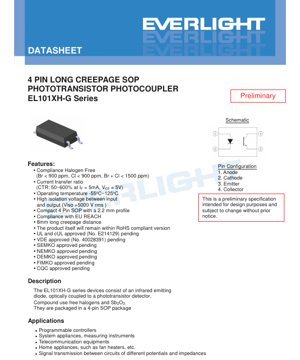
5.1 Pin Configuration
The 4-pin SOP package has the following pinout:
- Anode of the input infrared LED.
- Cathode of the input infrared LED.
- Emitter of the output phototransistor.
- Collector of the output phototransistor.
5.2 Package Dimensions and Footprint
The device is described as a "Compact 4 Pin SOP with a 2.2 mm profile." The PDF includes a "Package Dimension" diagram and a "Recommended pad layout for surface mount." The pad layout suggestion is provided as a reference, and the datasheet explicitly advises designers to modify the pad dimensions based on their specific PCB manufacturing processes and thermal requirements. Proper pad design is essential for reliable soldering and mechanical strength.
6. Soldering and Assembly Guidelines
The key parameter provided is the soldering temperature: 260°C for 10 seconds. This aligns with typical lead-free reflow soldering profiles (IPC/JEDEC J-STD-020). Designers and manufacturers must ensure their reflow oven profile does not exceed this time-at-temperature to prevent damage to the internal epoxy mold compound and the wire bonds. Standard handling procedures for moisture-sensitive devices (MSL rating, which is not specified in the provided text but should be checked in the full datasheet) should be followed, including baking if the packaging has been exposed to ambient humidity beyond its rated level.
7. Packaging and Ordering Information
7.1 Model Numbering Rule
The part number follows the format: EL101X H(Y)- VG
- EL101: Base part number.
- X: CTR Rank (0, 1, 7, 8, 9).
- H: Denotes high-temperature operation capability.
- (Y): Tape and reel option. Can be TA, TB, or none (for tube packaging).
- V: Optional suffix denoting VDE safety certification.
- G: Denotes halogen-free construction.
7.2 Packaging Specifications
The device is available in two main packaging forms:
- Tube: 100 units per tube. Options are standard or with VDE certification.
- Tape and Reel: 3000 units per reel. Two feed direction options are available (TA and TB), with detailed tape dimensions (Ao, Bo, Po, P, etc.) provided in the datasheet for automated pick-and-place machine programming.
7.3 Device Marking
The top of the SOP package is marked with a code: EL 101X H Y WW V
- EL: Manufacturer code.
- 101X: Device number (X indicates CTR rank).
- H: High-temperature operating designation.
- Y: 1-digit year code.
- WW: 2-digit week code.
- V: Optional marking for VDE-approved versions.
8. Application Recommendations
8.1 Typical Application Circuits
The photocoupler can be used in two primary modes:
- Digital Switching / Isolation: The input LED is driven by a digital signal (e.g., from a microcontroller GPIO). The phototransistor output acts as a switch, pulling a line to ground or VCC through a pull-up resistor. The switching time specifications determine the maximum data rate.
- Linear Signal Isolation: By operating the phototransistor in its active region (not saturated), it can be used to transmit analog signals. However, the non-linear CTR and its variation with temperature make this challenging without additional compensation circuitry. It is more common to use a dedicated linear optocoupler for such tasks.
8.2 Design Considerations
- Input Current Limiting: An external resistor is always required in series with the input LED to set the forward current (IF). Calculate Rlimit = (Vdrive - VF) / IF. Ensure IF does not exceed 50 mA DC.
- CTR Derating with Temperature: Account for the decrease in CTR at high temperatures. Design the circuit to function correctly at the maximum operating temperature with the minimum CTR from the selected grade.
- Output Load Resistor (RL): The value of the pull-up resistor on the collector affects switching speed, power consumption, and noise immunity. A smaller RL gives faster switching but higher current draw. The test condition of RL = 100Ω is for characterization; practical values often range from 1kΩ to 10kΩ.
- Noise Immunity: The low coupling capacitance (<1pF) provides good common-mode rejection. For very noisy environments, ensure a clean layout with proper grounding and consider adding a small bypass capacitor (e.g., 0.1µF) across the output side supply rails.
9. Technical Comparison and Advantages
The EL101XH-G series differentiates itself in the market through several key features:
- Long Creepage Distance (8mm): Compared to standard SOP optocouplers, this extended creepage is a significant advantage for applications requiring reinforced insulation or operating in polluted environments, as it reduces the risk of surface tracking.
- High Isolation Voltage (5000Vrms): This is a robust isolation rating suitable for industrial mains-connected equipment (e.g., 240V/480V systems).
- Halogen-Free Compliance: Meets environmental and regulatory requirements for reduced halogen content, which is increasingly important in green electronics.
- Wide Operating Temperature Range (-55°C to +125°C): Exceeds the typical commercial range (0°C to 70°C), making it fit for industrial, automotive, and military-grade applications.
- Pending Safety Approvals: The datasheet lists approvals from UL, cUL, VDE, SEMKO, NEMKO, DEMKO, FIMKO, and CQC as "pending." This indicates the device is designed to meet these stringent international safety standards.
10. Frequently Asked Questions (Based on Technical Parameters)
Q1: What is the purpose of the long creepage distance?
A1: Creepage distance is the shortest path along the surface of the insulating package between two conductive parts (input and output pins). An 8mm distance increases protection against high-voltage arcing or tracking across the package surface, especially in humid or contaminated environments, enhancing long-term reliability and safety.
Q2: How do I choose the right CTR grade?
A2: Select based on your available drive current and required output current. If your microcontroller can only provide 5mA, choose a high-CTR grade (e.g., EL1019H) to get sufficient output current. If you have ample drive current, a lower grade may be more cost-effective. Always design for the worst-case (minimum CTR at maximum temperature).
Q3: Can this be used for AC signal isolation?
A3: The phototransistor output is unidirectional (current flows from Collector to Emitter). To isolate an AC signal, you would typically use two devices in inverse-parallel configuration or a dedicated AC-input optocoupler. For digital AC zero-crossing detection, it can be used with a bridge rectifier on the input.
Q4: What is the difference between isolation voltage and collector-emitter voltage rating?
A4: Isolation voltage (5000Vrms) is the dielectric withstand voltage between the input and output sides of the package. Collector-emitter voltage (80V) is the maximum voltage that can be applied across the output transistor itself during normal operation. They are completely different parameters.
11. Practical Design Case Study
Scenario: Isolating a 3.3V microcontroller GPIO signal to control a 24V relay coil on a separate power domain in an industrial PLC module.
Design Steps:
- Input Side: The MCU GPIO is 3.3V. Assuming a desired IF of 5mA and a typical VF of 1.2V, calculate Rlimit = (3.3V - 1.2V) / 0.005A = 420Ω. Use a standard 430Ω resistor.
- CTR Selection: The relay coil driver transistor base requires ~5mA. With IF=5mA, minimum required CTR = (5mA / 5mA)*100% = 100%. To ensure operation at 125°C (where CTR is lower), select a grade with comfortable margin. EL1018H (min CTR 130%) is a good choice.
- Output Side: Connect the phototransistor collector to the 24V supply via a pull-up resistor (RL). The emitter connects to the base of the relay driver transistor (an NPN BJT or an N-channel MOSFET gate). When the MCU output is high, the LED is on, the phototransistor saturates, pulling the base to near ground, turning off the driver. When the MCU output is low, the LED is off, the phototransistor is off, and a separate bias resistor pulls the driver base high to activate the relay. A snubber diode is required across the relay coil.
- Layout: Keep the input and output traces physically separated on the PCB. Place the bypass capacitors close to the device pins. Follow the recommended pad layout for reliable soldering.
12. Operating Principle
A photocoupler (or optocoupler) is a device that transfers electrical signals between two isolated circuits using light. In the EL101XH-G series:
- An electrical current applied to the input pins (Anode and Cathode) causes the integrated infrared light-emitting diode (LED) to emit photons.
- These photons travel through a transparent insulating material (typically a molded epoxy) within the package.
- The photons strike the base region of a silicon phototransistor on the output side.
- This light energy generates electron-hole pairs in the base, effectively acting as a base current and causing the transistor to conduct between its Collector and Emitter pins.
- The amount of output collector current (IC) is proportional to the input LED current (IF), with the proportionality constant being the Current Transfer Ratio (CTR).
13. Industry Trends
The market for isolation components like photocouplers is evolving driven by several key trends:
- Higher Speed and Bandwidth: Demand is growing for digital isolators and high-speed optocouplers capable of supporting communication protocols like USB, CAN FD, and Ethernet in isolated networks, pushing data rates into the tens and hundreds of Mbps.
- Integration: There is a trend towards integrating multiple isolation channels into a single package, or combining isolation with other functions like gate drivers for power MOSFETs/IGBTs.
- Enhanced Safety and Reliability Standards: Regulations in industrial, automotive (ISO 26262), and medical equipment continue to tighten, requiring components with higher certified isolation ratings, longer creepage/clearance, and proven reliability data.
- Miniaturization: While maintaining or improving isolation performance, packages are becoming smaller (e.g., wide-body SOIC, DSOP) to save board space.
- Alternative Technologies: Photocouplers face competition from capacitive and magnetic (transformer-based) isolation technologies, which can offer advantages in speed, power consumption, and integration. However, optocouplers retain strong advantages in simplicity, high common-mode transient immunity (CMTI), and well-established safety certifications.
LED Specification Terminology
Complete explanation of LED technical terms
Photoelectric Performance
| Term | Unit/Representation | Simple Explanation | Why Important |
|---|---|---|---|
| Luminous Efficacy | lm/W (lumens per watt) | Light output per watt of electricity, higher means more energy efficient. | Directly determines energy efficiency grade and electricity cost. |
| Luminous Flux | lm (lumens) | Total light emitted by source, commonly called "brightness". | Determines if the light is bright enough. |
| Viewing Angle | ° (degrees), e.g., 120° | Angle where light intensity drops to half, determines beam width. | Affects illumination range and uniformity. |
| CCT (Color Temperature) | K (Kelvin), e.g., 2700K/6500K | Warmth/coolness of light, lower values yellowish/warm, higher whitish/cool. | Determines lighting atmosphere and suitable scenarios. |
| CRI / Ra | Unitless, 0–100 | Ability to render object colors accurately, Ra≥80 is good. | Affects color authenticity, used in high-demand places like malls, museums. |
| SDCM | MacAdam ellipse steps, e.g., "5-step" | Color consistency metric, smaller steps mean more consistent color. | Ensures uniform color across same batch of LEDs. |
| Dominant Wavelength | nm (nanometers), e.g., 620nm (red) | Wavelength corresponding to color of colored LEDs. | Determines hue of red, yellow, green monochrome LEDs. |
| Spectral Distribution | Wavelength vs intensity curve | Shows intensity distribution across wavelengths. | Affects color rendering and quality. |
Electrical Parameters
| Term | Symbol | Simple Explanation | Design Considerations |
|---|---|---|---|
| Forward Voltage | Vf | Minimum voltage to turn on LED, like "starting threshold". | Driver voltage must be ≥Vf, voltages add up for series LEDs. |
| Forward Current | If | Current value for normal LED operation. | Usually constant current drive, current determines brightness & lifespan. |
| Max Pulse Current | Ifp | Peak current tolerable for short periods, used for dimming or flashing. | Pulse width & duty cycle must be strictly controlled to avoid damage. |
| Reverse Voltage | Vr | Max reverse voltage LED can withstand, beyond may cause breakdown. | Circuit must prevent reverse connection or voltage spikes. |
| Thermal Resistance | Rth (°C/W) | Resistance to heat transfer from chip to solder, lower is better. | High thermal resistance requires stronger heat dissipation. |
| ESD Immunity | V (HBM), e.g., 1000V | Ability to withstand electrostatic discharge, higher means less vulnerable. | Anti-static measures needed in production, especially for sensitive LEDs. |
Thermal Management & Reliability
| Term | Key Metric | Simple Explanation | Impact |
|---|---|---|---|
| Junction Temperature | Tj (°C) | Actual operating temperature inside LED chip. | Every 10°C reduction may double lifespan; too high causes light decay, color shift. |
| Lumen Depreciation | L70 / L80 (hours) | Time for brightness to drop to 70% or 80% of initial. | Directly defines LED "service life". |
| Lumen Maintenance | % (e.g., 70%) | Percentage of brightness retained after time. | Indicates brightness retention over long-term use. |
| Color Shift | Δu′v′ or MacAdam ellipse | Degree of color change during use. | Affects color consistency in lighting scenes. |
| Thermal Aging | Material degradation | Deterioration due to long-term high temperature. | May cause brightness drop, color change, or open-circuit failure. |
Packaging & Materials
| Term | Common Types | Simple Explanation | Features & Applications |
|---|---|---|---|
| Package Type | EMC, PPA, Ceramic | Housing material protecting chip, providing optical/thermal interface. | EMC: good heat resistance, low cost; Ceramic: better heat dissipation, longer life. |
| Chip Structure | Front, Flip Chip | Chip electrode arrangement. | Flip chip: better heat dissipation, higher efficacy, for high-power. |
| Phosphor Coating | YAG, Silicate, Nitride | Covers blue chip, converts some to yellow/red, mixes to white. | Different phosphors affect efficacy, CCT, and CRI. |
| Lens/Optics | Flat, Microlens, TIR | Optical structure on surface controlling light distribution. | Determines viewing angle and light distribution curve. |
Quality Control & Binning
| Term | Binning Content | Simple Explanation | Purpose |
|---|---|---|---|
| Luminous Flux Bin | Code e.g., 2G, 2H | Grouped by brightness, each group has min/max lumen values. | Ensures uniform brightness in same batch. |
| Voltage Bin | Code e.g., 6W, 6X | Grouped by forward voltage range. | Facilitates driver matching, improves system efficiency. |
| Color Bin | 5-step MacAdam ellipse | Grouped by color coordinates, ensuring tight range. | Guarantees color consistency, avoids uneven color within fixture. |
| CCT Bin | 2700K, 3000K etc. | Grouped by CCT, each has corresponding coordinate range. | Meets different scene CCT requirements. |
Testing & Certification
| Term | Standard/Test | Simple Explanation | Significance |
|---|---|---|---|
| LM-80 | Lumen maintenance test | Long-term lighting at constant temperature, recording brightness decay. | Used to estimate LED life (with TM-21). |
| TM-21 | Life estimation standard | Estimates life under actual conditions based on LM-80 data. | Provides scientific life prediction. |
| IESNA | Illuminating Engineering Society | Covers optical, electrical, thermal test methods. | Industry-recognized test basis. |
| RoHS / REACH | Environmental certification | Ensures no harmful substances (lead, mercury). | Market access requirement internationally. |
| ENERGY STAR / DLC | Energy efficiency certification | Energy efficiency and performance certification for lighting. | Used in government procurement, subsidy programs, enhances competitiveness. |