Table of Contents
- 1. Product Overview
- 2. Technical Parameters Deep Dive
- 2.1 Photometric & Electrical Characteristics
- 2.2 Absolute Maximum Ratings
- 2.3 Thermal Characteristics
- 3. Performance Curve Analysis
- 3.1 Forward Current vs. Voltage (I-V Curve)
- 3.2 Optical Output vs. Current and Temperature
- 3.3 Chromaticity Stability
- 3.4 Spectral Distribution and Radiation Pattern
- 4. Binning System Explanation
- 4.1 Luminous Intensity Binning
- 4.2 Color Binning
- 5. Mechanical & Packaging Information
- 5.1 Physical Dimensions
- 5.2 Recommended Solder Pad Layout
- 5.3 Polarity Identification
- 6. Soldering & Assembly Guidelines
- 6.1 Reflow Soldering Profile
- 6.2 Precautions for Use
- 6.3 Storage Conditions
- 7. Application Recommendations
- 7.1 Typical Application Circuits
- 7.2 Design Considerations
- 8. Technical Comparison & Differentiation
- 9. Frequently Asked Questions (FAQs)
- 10. Operating Principle
- 11. Industry Trends
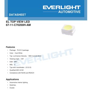
1. Product Overview
This document details the specifications for a high-brightness, surface-mount LED component utilizing the PLCC-2 (Plastic Leaded Chip Carrier) package. The device is engineered primarily for demanding automotive interior environments, offering reliable performance under a wide temperature range. Its core advantages include a balanced combination of luminous output, wide viewing angle, and robust construction meeting automotive-grade reliability standards.
The LED emits a cool white light, characterized by typical CIE 1931 color coordinates of (0.3, 0.3). It is targeted at applications requiring consistent, bright illumination in confined spaces, such as dashboard backlighting, switch illumination, and indicator clusters. Compliance with AEC-Q102, RoHS, and REACH underscores its suitability for modern electronic assemblies with stringent quality and environmental requirements.
2. Technical Parameters Deep Dive
2.1 Photometric & Electrical Characteristics
The key operating parameters are defined at a standard test current of 20mA. The typical luminous intensity is 1800 millicandelas (mcd), with a minimum guaranteed value of 1400 mcd and a maximum up to 3550 mcd depending on the production bin. The forward voltage (VF) typically measures 3.1V, ranging from a minimum of 2.5V to a maximum of 3.75V. This parameter is crucial for calculating current-limiting resistor values in circuit design.
The device features a very wide viewing angle of 120 degrees, defined as the full angle where luminous intensity drops to half of its peak axial value. This ensures uniform light distribution, which is essential for panel and switch illumination.
2.2 Absolute Maximum Ratings
These ratings define the stress limits beyond which permanent damage may occur. The absolute maximum continuous forward current is 30 mA. The device can withstand short current surges up to 250 mA for pulses \u2264 10 \u00b5s with a very low duty cycle (0.005). The junction temperature must not exceed 125\u00b0C. The operating and storage temperature range is specified from -40\u00b0C to +110\u00b0C, confirming its automotive-grade robustness. Electrostatic discharge (ESD) protection is rated at 8 kV (Human Body Model).
2.3 Thermal Characteristics
Thermal management is critical for LED longevity and performance stability. The thermal resistance from the junction to the solder point is specified in two ways: a real thermal resistance (Rth JS real) of 130 K/W and an electrical thermal resistance (Rth JS el) of 100 K/W. This parameter indicates how effectively heat is conducted away from the semiconductor junction. Proper PCB layout with adequate thermal relief is necessary to maintain the solder pad temperature within safe limits, as shown in the derating curve.
3. Performance Curve Analysis
3.1 Forward Current vs. Voltage (I-V Curve)
The provided graph shows the relationship between forward current and forward voltage at 25\u00b0C. The curve is non-linear, typical of a diode. At the nominal 20mA, the voltage is centered around 3.1V. Designers must use this curve to ensure the driver circuit provides stable current, not voltage, to achieve consistent light output.
3.2 Optical Output vs. Current and Temperature
The relative luminous intensity increases with forward current but exhibits a sub-linear relationship, emphasizing the need for current control. More importantly, the graph showing relative luminous intensity vs. junction temperature demonstrates a negative temperature coefficient. As the junction temperature rises, the light output decreases. At the maximum junction temperature of 125\u00b0C, the output may be only around 40-50% of its value at 25\u00b0C. This thermal quenching effect must be accounted for in thermal design.
3.3 Chromaticity Stability
Graphs depict the shift in CIE x and y coordinates with both forward current and junction temperature. While shifts are present, they are relatively small (\u00b1~0.01 for temperature, less for current), indicating good color stability under varying operating conditions, which is vital for applications where color consistency is important.
3.4 Spectral Distribution and Radiation Pattern
The relative spectral distribution curve shows a peak in the blue wavelength region, characteristic of a phosphor-converted white LED, with a broad secondary peak in the yellow/green region from the phosphor. The radiation pattern diagram confirms the Lambertian-like emission profile, resulting in the wide 120\u00b0 viewing angle.
4. Binning System Explanation
The product is available in sorted performance groups, or "bins," to ensure consistency within a production lot.
4.1 Luminous Intensity Binning
A comprehensive binning structure is defined, ranging from low-output bins (e.g., L1: 11.2-14 mcd) to very high-output bins (e.g., GA: 18000-22400 mcd). For this specific part number (67-11-C70200H-AM), the highlighted standard output bin is "AB," which corresponds to a luminous intensity range of 1400 to 1800 mcd. This allows designers to select the appropriate brightness grade for their application.
4.2 Color Binning
The datasheet references a "Standard White Color Bin Structure" diagram (not fully detailed in the provided excerpt). Typically, such diagrams plot the CIE x and y coordinates within a defined quadrilateral or region on the chromaticity chart. LEDs are sorted into bins based on where their color coordinates fall within this region, ensuring a tight color tolerance, typically within \u00b10.005 as noted in the characteristics section.
5. Mechanical & Packaging Information
5.1 Physical Dimensions
The component uses a standard PLCC-2 surface-mount package. The mechanical drawing (referenced in the contents) would specify the exact length, width, height, lead spacing, and tolerances. This information is critical for PCB footprint design and ensuring proper fit within the assembly.
5.2 Recommended Solder Pad Layout
A dedicated section provides the recommended land pattern (solder pad geometry) for the PCB. Following this guideline is essential for achieving reliable solder joints, proper self-alignment during reflow, and effective heat transfer from the device to the PCB.
5.3 Polarity Identification
PLCC-2 packages typically have a marked corner or a chamfer to indicate the cathode (negative) pin. Correct polarity orientation is mandatory during placement to ensure the device functions.
6. Soldering & Assembly Guidelines
6.1 Reflow Soldering Profile
The datasheet specifies a maximum soldering temperature of 260\u00b0C for 30 seconds. This refers to the peak temperature measured at the solder joints during a standard reflow process. A typical reflow profile with preheat, soak, reflow, and cooling stages should be followed, ensuring the temperature at the component leads does not exceed this limit to prevent damage to the plastic package or the internal die attach.
6.2 Precautions for Use
General handling precautions include using ESD-safe practices during assembly, avoiding mechanical stress on the lens, and preventing contamination of the optical surface. The device is not designed for reverse voltage operation.
6.3 Storage Conditions
The storage temperature range is -40\u00b0C to +110\u00b0C. Furthermore, the Moisture Sensitivity Level (MSL) is rated as Level 2. This means the component can be stored in a dry environment (typically < 60% Relative Humidity) for up to one year. If the moisture barrier bag is opened or exceeded, the parts must be baked before reflow soldering to prevent "popcorning" (package cracking due to vapor pressure).
7. Application Recommendations
7.1 Typical Application Circuits
The most common drive method is a constant current source or a simple series resistor from a voltage rail. The resistor value is calculated as R = (Vsupply - VF) / IF. Using the typical VF of 3.1V and a 20mA target, with a 5V supply, the resistor would be (5V - 3.1V) / 0.02A = 95 Ohms. A resistor rated for at least (5V-3.1V)*0.02A = 0.038W should be selected, with a higher wattage (e.g., 1/8W or 1/4W) for safety margin.
7.2 Design Considerations
- Thermal Management: Use the forward current derating curve. For continuous operation at high ambient temperatures, the current must be reduced to keep the solder point temperature below 110\u00b0C (where max current is 30mA). Adequate copper area under and around the solder pads is necessary to dissipate heat.
- Current Control: Always drive LEDs with a controlled current, not a fixed voltage, to ensure stable light output and prevent thermal runaway.
- Optical Design: The wide 120\u00b0 beam is suitable for diffuse lighting. For focused light, secondary optics (lenses) would be required.
- ESD Protection: While the device has 8kV HBM protection, incorporating additional transient voltage suppression on sensitive lines in automotive environments is good practice.
8. Technical Comparison & Differentiation
Compared to generic PLCC-2 LEDs, this device's key differentiators are its AEC-Q102 qualification and extended operating temperature range (-40\u00b0C to +110\u00b0C). These are not typical for commercial-grade LEDs and are essential for automotive certification. The specified ESD rating (8kV) is also higher than many standard parts. The detailed binning structure provides manufacturers with predictable performance, which is critical for mass production where consistency is paramount.
9. Frequently Asked Questions (FAQs)
Q: What is the difference between "Typical" and "Maximum" ratings?
A: "Typical" is the expected average value under standard conditions. "Maximum" (or "Min") are the guaranteed limits; all devices will perform within these bounds as per the datasheet specification.
Q: Can I drive this LED at 30mA continuously?
A: Only if the solder pad temperature (TS) can be maintained at or below 110\u00b0C, as per the derating curve. At higher temperatures, the current must be reduced. For reliable long-term operation, driving at or below the typical 20mA is recommended.
Q: The color coordinates are (0.3, 0.3). Is this a pure white?
A: On the CIE 1931 chromaticity diagram, the point (0.33, 0.33) is often considered the "equal energy" white point. Coordinates of (0.3, 0.3) indicate a cool white with a slight shift towards blue/green, which is a common and desirable tone for display backlighting.
Q: What does MSL 2 mean for my production process?
A: MSL 2 components have a floor life of 1 year when stored at \u2264 30\u00b0C/60% RH. After the bag is opened, they should be used within a specified time (e.g., 168 hours) or baked before reflow to remove absorbed moisture.
10. Operating Principle
This is a phosphor-converted white LED. The core semiconductor chip emits blue light when current flows across its p-n junction (electroluminescence). This blue light strikes a layer of yellow (or yellow and red) phosphor material deposited on or near the chip. The phosphor absorbs a portion of the blue photons and re-emits light at longer, yellow/red wavelengths. The combination of the remaining blue light and the converted yellow/red light is perceived by the human eye as white light. The exact shade (cool white, neutral white, warm white) is determined by the blend and composition of the phosphors.
11. Industry Trends
The automotive lighting market continues to demand higher efficiency (more lumens per watt), improved color rendering index (CRI) for better visual clarity, and greater reliability. Integration of LEDs with driver ICs and sensors into smart lighting modules is a growing trend. Furthermore, there is a push towards standardized, smaller package footprints with higher power density, although PLCC packages remain popular for their cost-effectiveness and proven reliability in mid-power applications like interior lighting.
LED Specification Terminology
Complete explanation of LED technical terms
Photoelectric Performance
| Term | Unit/Representation | Simple Explanation | Why Important |
|---|---|---|---|
| Luminous Efficacy | lm/W (lumens per watt) | Light output per watt of electricity, higher means more energy efficient. | Directly determines energy efficiency grade and electricity cost. |
| Luminous Flux | lm (lumens) | Total light emitted by source, commonly called "brightness". | Determines if the light is bright enough. |
| Viewing Angle | ° (degrees), e.g., 120° | Angle where light intensity drops to half, determines beam width. | Affects illumination range and uniformity. |
| CCT (Color Temperature) | K (Kelvin), e.g., 2700K/6500K | Warmth/coolness of light, lower values yellowish/warm, higher whitish/cool. | Determines lighting atmosphere and suitable scenarios. |
| CRI / Ra | Unitless, 0–100 | Ability to render object colors accurately, Ra≥80 is good. | Affects color authenticity, used in high-demand places like malls, museums. |
| SDCM | MacAdam ellipse steps, e.g., "5-step" | Color consistency metric, smaller steps mean more consistent color. | Ensures uniform color across same batch of LEDs. |
| Dominant Wavelength | nm (nanometers), e.g., 620nm (red) | Wavelength corresponding to color of colored LEDs. | Determines hue of red, yellow, green monochrome LEDs. |
| Spectral Distribution | Wavelength vs intensity curve | Shows intensity distribution across wavelengths. | Affects color rendering and quality. |
Electrical Parameters
| Term | Symbol | Simple Explanation | Design Considerations |
|---|---|---|---|
| Forward Voltage | Vf | Minimum voltage to turn on LED, like "starting threshold". | Driver voltage must be ≥Vf, voltages add up for series LEDs. |
| Forward Current | If | Current value for normal LED operation. | Usually constant current drive, current determines brightness & lifespan. |
| Max Pulse Current | Ifp | Peak current tolerable for short periods, used for dimming or flashing. | Pulse width & duty cycle must be strictly controlled to avoid damage. |
| Reverse Voltage | Vr | Max reverse voltage LED can withstand, beyond may cause breakdown. | Circuit must prevent reverse connection or voltage spikes. |
| Thermal Resistance | Rth (°C/W) | Resistance to heat transfer from chip to solder, lower is better. | High thermal resistance requires stronger heat dissipation. |
| ESD Immunity | V (HBM), e.g., 1000V | Ability to withstand electrostatic discharge, higher means less vulnerable. | Anti-static measures needed in production, especially for sensitive LEDs. |
Thermal Management & Reliability
| Term | Key Metric | Simple Explanation | Impact |
|---|---|---|---|
| Junction Temperature | Tj (°C) | Actual operating temperature inside LED chip. | Every 10°C reduction may double lifespan; too high causes light decay, color shift. |
| Lumen Depreciation | L70 / L80 (hours) | Time for brightness to drop to 70% or 80% of initial. | Directly defines LED "service life". |
| Lumen Maintenance | % (e.g., 70%) | Percentage of brightness retained after time. | Indicates brightness retention over long-term use. |
| Color Shift | Δu′v′ or MacAdam ellipse | Degree of color change during use. | Affects color consistency in lighting scenes. |
| Thermal Aging | Material degradation | Deterioration due to long-term high temperature. | May cause brightness drop, color change, or open-circuit failure. |
Packaging & Materials
| Term | Common Types | Simple Explanation | Features & Applications |
|---|---|---|---|
| Package Type | EMC, PPA, Ceramic | Housing material protecting chip, providing optical/thermal interface. | EMC: good heat resistance, low cost; Ceramic: better heat dissipation, longer life. |
| Chip Structure | Front, Flip Chip | Chip electrode arrangement. | Flip chip: better heat dissipation, higher efficacy, for high-power. |
| Phosphor Coating | YAG, Silicate, Nitride | Covers blue chip, converts some to yellow/red, mixes to white. | Different phosphors affect efficacy, CCT, and CRI. |
| Lens/Optics | Flat, Microlens, TIR | Optical structure on surface controlling light distribution. | Determines viewing angle and light distribution curve. |
Quality Control & Binning
| Term | Binning Content | Simple Explanation | Purpose |
|---|---|---|---|
| Luminous Flux Bin | Code e.g., 2G, 2H | Grouped by brightness, each group has min/max lumen values. | Ensures uniform brightness in same batch. |
| Voltage Bin | Code e.g., 6W, 6X | Grouped by forward voltage range. | Facilitates driver matching, improves system efficiency. |
| Color Bin | 5-step MacAdam ellipse | Grouped by color coordinates, ensuring tight range. | Guarantees color consistency, avoids uneven color within fixture. |
| CCT Bin | 2700K, 3000K etc. | Grouped by CCT, each has corresponding coordinate range. | Meets different scene CCT requirements. |
Testing & Certification
| Term | Standard/Test | Simple Explanation | Significance |
|---|---|---|---|
| LM-80 | Lumen maintenance test | Long-term lighting at constant temperature, recording brightness decay. | Used to estimate LED life (with TM-21). |
| TM-21 | Life estimation standard | Estimates life under actual conditions based on LM-80 data. | Provides scientific life prediction. |
| IESNA | Illuminating Engineering Society | Covers optical, electrical, thermal test methods. | Industry-recognized test basis. |
| RoHS / REACH | Environmental certification | Ensures no harmful substances (lead, mercury). | Market access requirement internationally. |
| ENERGY STAR / DLC | Energy efficiency certification | Energy efficiency and performance certification for lighting. | Used in government procurement, subsidy programs, enhances competitiveness. |