Table of Contents
- 1. Product Overview
- 2. In-Depth Technical Parameter Analysis
- 2.1 Absolute Maximum Ratings
- 2.2 Electro-Optical Characteristics
- 3. Performance Curve Analysis
- 3.1 Spectral Sensitivity
- 3.2 Dark Current vs. Ambient Temperature
- 3.3 Reverse Light Current vs. Irradiance
- 3.4 Terminal Capacitance vs. Reverse Voltage
- 3.5 Response Time vs. Load Resistance
- 3.6 Relative Light Current vs. Angular Displacement
- 4. Mechanical and Package Information
- 4.1 Package Dimensions
- 4.2 Carrier Tape and Reel Dimensions
- 5. Soldering and Assembly Guidelines
- 5.1 Storage and Moisture Sensitivity
- 5.2 Reflow Soldering Profile
- 5.3 Hand Soldering and Rework
- 6. Application Notes and Design Considerations
- 6.1 Typical Applications
- 6.2 Critical Design Considerations
- 7. Packaging and Ordering Information
- 8. Technical Comparison and Positioning
- 9. Frequently Asked Questions (FAQ)
- 10. Operational Principle
- 11. Industry Trends
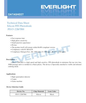
1. Product Overview
The PD15-22B/TR8 is a high-speed, high-sensitivity silicon PIN photodiode designed for applications requiring fast optical detection. It is housed in a miniature, flat-top surface-mount device (SMD) package with a black plastic molding and a black lens. The device is spectrally matched to visible and near-infrared light sources, making it suitable for a variety of sensing applications.
Key advantages of this component include its fast response time, which enables it to detect rapid changes in light intensity, and its high photosensitivity, allowing for reliable operation even under low-light conditions. The small junction capacitance contributes to its high-speed performance. The product is compliant with environmental standards, being lead-free (Pb-free), RoHS compliant, EU REACH compliant, and halogen-free (with Bromine <900 ppm, Chlorine <900 ppm, Br+Cl < 1500 ppm).
2. In-Depth Technical Parameter Analysis
2.1 Absolute Maximum Ratings
The device is designed to operate reliably within specified limits. Exceeding these Absolute Maximum Ratings may cause permanent damage.
- Reverse Voltage (VR): 32 V. This is the maximum voltage that can be applied in the reverse-biased condition without causing breakdown.
- Operating Temperature (Topr): -40°C to +85°C. This defines the ambient temperature range for normal device operation.
- Storage Temperature (Tstg): -40°C to +100°C. The device can be stored within this range when not in operation.
- Soldering Temperature (Tsol): 260°C for a maximum of 5 seconds. This is critical for reflow soldering processes.
- Power Dissipation (Pc): 150 mW. The maximum power the device can safely dissipate.
- ESD HMB Level: Minimum 2000V. Indicates the device's robustness against electrostatic discharge using the Human Body Model.
2.2 Electro-Optical Characteristics
These parameters are measured at Ta=25°C and define the core performance of the photodiode.
- Spectral Bandwidth (λ): 730 nm to 1100 nm (at 10% of peak sensitivity). The device responds to light within this wavelength range, with peak sensitivity in the near-infrared.
- Peak Sensitivity Wavelength (λP): Typically 940 nm. The wavelength at which the photodiode is most sensitive.
- Open-Circuit Voltage (VOC): Typically 0.41 V under an irradiance (Ee) of 5 mW/cm² at λP=940nm. This is the voltage generated when the terminals are open.
- Short-Circuit Current (ISC): Minimum 4.0 μA, Typical 6.5 μA under Ee=1 mW/cm² at λP=875nm. This is the current generated when the terminals are shorted.
- Reverse Light Current (IL): Minimum 4.2 μA, Typical 6.5 μA under Ee=1 mW/cm² at λP=875nm and VR=5V. This is the photocurrent generated when the diode is reverse-biased, which is the typical operating mode for high-speed applications.
- Dark Reverse Current (ID): Maximum 10 nA at VR=10V in complete darkness. This is the small leakage current that flows even when no light is present.
- Reverse Breakdown Voltage (BVR): Minimum 32 V, Typical 170 V measured at a reverse current (IR) of 100 μA in darkness.
- Rise/Fall Time (tr, tf): Typically 10 ns each under VR=5V and RL=1000 Ω. This defines the switching speed of the photodiode.
- View Angle (2θ1/2): Typically 130 degrees at VR=5V. This indicates a wide field of view for light detection.
3. Performance Curve Analysis
The datasheet provides several characteristic curves that are essential for design engineers.
3.1 Spectral Sensitivity
The spectral response curve shows the relative sensitivity of the photodiode across different wavelengths. It confirms peak sensitivity around 940 nm, with useful response from 730 nm to 1100 nm. This makes it an ideal match for infrared emitters like those with 850nm or 940nm wavelengths commonly used in remote controls, proximity sensors, and data communication links.
3.2 Dark Current vs. Ambient Temperature
This curve illustrates how the dark current (ID) increases exponentially with rising ambient temperature. At 25°C, it is below 10 nA, but it can rise significantly at higher temperatures (e.g., 85°C). Designers must account for this increased noise floor in high-temperature applications or when very low light levels need to be detected.
3.3 Reverse Light Current vs. Irradiance
This graph shows the linear relationship between the reverse light current (IL) and the incident light irradiance (Ee). The photodiode exhibits good linearity, meaning the output current is directly proportional to the light intensity over its operating range. This is crucial for analog light sensing applications where accurate intensity measurement is required.
3.4 Terminal Capacitance vs. Reverse Voltage
The junction capacitance decreases as the reverse bias voltage (VR) increases. A lower capacitance is desirable for high-speed operation as it reduces the RC time constant of the circuit. The curve shows that applying a higher reverse bias (e.g., 10V instead of 5V) can significantly reduce capacitance, thereby improving bandwidth and response time.
3.5 Response Time vs. Load Resistance
This curve demonstrates the trade-off between response speed and signal amplitude. The rise/fall time increases with higher load resistance (RL). For the fastest response, a low-value load resistor (e.g., 50 Ω) should be used, but this will produce a smaller voltage signal. A transimpedance amplifier is often used to overcome this limitation, providing both high speed and good signal gain.
3.6 Relative Light Current vs. Angular Displacement
This plot characterizes the angular sensitivity of the photodiode. The wide 130-degree view angle is confirmed, showing that the detected signal remains relatively high even for light incident at significant angles off the central axis. This is beneficial for applications where alignment is not perfect or where a wide detection field is needed.
4. Mechanical and Package Information
4.1 Package Dimensions
The PD15-22B/TR8 comes in a compact SMD package. Key dimensions are as follows (all in mm, tolerances ±0.1mm unless specified):
- Overall Length: 4.0 mm
- Overall Width: 3.5 mm
- Overall Height: 1.65 mm (typical, from seating plane to top of lens)
- Lead Width: 1.55 mm ±0.05 mm
- Lead Pitch: 2.95 mm
- Terminal land pattern recommendations are provided for PCB layout.
The anode and cathode are clearly marked on the package drawing. Pin 1 is the cathode.
4.2 Carrier Tape and Reel Dimensions
The device is supplied on tape and reel for automated assembly. The reel contains 2000 pieces. Detailed dimensions for the carrier tape pockets and reel are provided to ensure compatibility with standard pick-and-place equipment.
5. Soldering and Assembly Guidelines
5.1 Storage and Moisture Sensitivity
The photodiode is moisture-sensitive. Precautions must be taken to prevent damage during storage and handling.
- Do not open the moisture-proof bag until ready for use.
- Before opening, store at ≤30°C and ≤90% RH.
- Use within one year of shipment.
- After opening, store at ≤30°C and ≤60% RH.
- Use within 168 hours (7 days) after opening the bag.
- If the storage time is exceeded or the desiccant indicates moisture, bake at 60 ±5°C for a minimum of 24 hours before use.
5.2 Reflow Soldering Profile
A recommended Pb-free reflow soldering temperature profile is provided. Key parameters include:
- Preheat and soak zone.
- Peak temperature not to exceed 260°C.
- Time above 240°C should be controlled.
- Reflow soldering should not be performed more than two times.
- Avoid mechanical stress on the component during heating.
- Do not warp the PCB after soldering.
5.3 Hand Soldering and Rework
If hand soldering is necessary:
- Use a soldering iron with a tip temperature <350°C.
- Limit contact time to ≤3 seconds per terminal.
- Use an iron with a power rating <25W.
- Allow a cooling interval of >2 seconds between soldering each terminal.
- Repair after soldering is not recommended. If unavoidable, use a dual-head soldering iron to simultaneously heat both terminals and minimize thermal stress. Verify device functionality after any rework.
6. Application Notes and Design Considerations
6.1 Typical Applications
- High-Speed Photo Detector: Suitable for optical data links, encoders, and laser detection due to its 10 ns response time.
- Copiers and Scanners: Used for detecting document presence, edge detection, and toner density sensing.
- Game Machines and Consumer Electronics: Employed in proximity sensing, gesture recognition, and IR remote control receivers.
6.2 Critical Design Considerations
- Current Limiting/Protection: The datasheet explicitly warns that an external series resistor MUST be used for protection. A slight voltage shift can cause a large current change, potentially leading to burnout. This resistor limits the current through the diode.
- Biasing for Speed: For optimal high-speed performance, operate the photodiode in reverse bias mode (photoconductive mode). A higher reverse voltage (up to the maximum rating) will reduce junction capacitance and improve response time, as shown in the characteristic curves.
- Circuit Topology: For converting the photocurrent to a voltage, consider using a transimpedance amplifier (TIA). This configuration provides low input impedance (keeping the photodiode voltage constant, which minimizes capacitance modulation), high bandwidth, and controllable gain. The choice of feedback resistor and amplifier bandwidth will determine the overall system performance.
- Optical Design: The black lens helps reduce stray light sensitivity. Ensure the optical path is clean and free from obstructions. The wide 130-degree view angle offers flexibility in mechanical alignment.
- Thermal Management: Account for the increase in dark current with temperature, especially in high-accuracy or high-temperature applications. Temperature compensation circuits may be necessary.
7. Packaging and Ordering Information
The standard packing procedure involves placing the reels into an aluminum moisture-proof bag along with a desiccant and appropriate labels. The label includes fields for Customer Part Number (CPN), Production Number (P/N), Quantity (QTY), Ranks (CAT), Peak Wavelength (HUE), Reference (REF), Lot Number (LOT No.), and Production Place.
The device selection guide confirms the model PD15-22B/TR8 uses a Silicon chip and has a Black lens.
8. Technical Comparison and Positioning
The PD15-22B/TR8 positions itself as a general-purpose, high-speed silicon PIN photodiode in a standard SMD package. Its key differentiators are its balanced combination of speed (10 ns), sensitivity, wide viewing angle, and robust environmental compliance (RoHS, Halogen-Free). Compared to slower photodiodes or phototransistors, it offers superior performance for pulsed light detection. Compared to more specialized, ultra-high-speed photodiodes, it provides a cost-effective solution for mainstream applications requiring response times in the nanosecond range. The black lens is an advantage over clear-lens versions in environments with ambient light, as it helps suppress unwanted signals.
9. Frequently Asked Questions (FAQ)
Q: What is the difference between Short-Circuit Current (ISC) and Reverse Light Current (IL)?
A: ISC is measured with zero voltage across the diode (short-circuit condition). IL is measured with a reverse bias voltage applied (e.g., 5V). IL is typically the parameter used in circuit design as photodiodes are usually operated in reverse bias for linearity and speed.
Q: Why is a series resistor mandatory?
A> The I-V characteristic of a photodiode is very steep in the forward direction. A small increase in forward voltage can cause a very large, potentially destructive, current to flow. The series resistor limits this current to a safe value.
Q: How do I choose the operating reverse voltage?
A> It involves a trade-off. A higher reverse voltage (e.g., 10-20V) reduces capacitance for faster response but increases dark current slightly and consumes more power. A lower voltage (e.g., 5V) is sufficient for many applications and keeps dark current minimal. Refer to the capacitance vs. voltage curve.
Q: Can this photodiode detect visible light?
A> Yes, its spectral range starts at 730 nm, which is in the deep red part of the visible spectrum. However, its peak sensitivity is in the near-infrared (940 nm), so its responsivity to visible light (especially blue and green) will be lower than to IR light.
10. Operational Principle
A PIN photodiode is a semiconductor device that converts light into electrical current. It consists of a wide, lightly doped intrinsic (I) region sandwiched between a P-type and an N-type semiconductor region (forming the P-I-N structure). When photons with sufficient energy strike the intrinsic region, they create electron-hole pairs. Under the influence of an internal electric field (often enhanced by an external reverse bias voltage), these charge carriers are swept apart, generating a photocurrent that is proportional to the incident light intensity. The wide intrinsic region allows for higher quantum efficiency (more light absorption) and lower junction capacitance compared to a standard PN photodiode, which directly translates to higher sensitivity and faster response times.
11. Industry Trends
The demand for photodiodes like the PD15-22B/TR8 is driven by several ongoing trends. The proliferation of the Internet of Things (IoT) and smart devices increases the need for ambient light sensors, proximity sensors, and simple optical communication links. Automation in industrial and consumer sectors relies on optical encoders and object detection sensors. There is a continuous push for miniaturization, leading to smaller SMD packages, and for higher integration, where photodiodes are combined with amplification and signal conditioning circuits in single modules. Furthermore, the emphasis on energy efficiency and environmental responsibility makes compliance with standards like RoHS and halogen-free manufacturing a baseline requirement for components used in global markets.
LED Specification Terminology
Complete explanation of LED technical terms
Photoelectric Performance
| Term | Unit/Representation | Simple Explanation | Why Important |
|---|---|---|---|
| Luminous Efficacy | lm/W (lumens per watt) | Light output per watt of electricity, higher means more energy efficient. | Directly determines energy efficiency grade and electricity cost. |
| Luminous Flux | lm (lumens) | Total light emitted by source, commonly called "brightness". | Determines if the light is bright enough. |
| Viewing Angle | ° (degrees), e.g., 120° | Angle where light intensity drops to half, determines beam width. | Affects illumination range and uniformity. |
| CCT (Color Temperature) | K (Kelvin), e.g., 2700K/6500K | Warmth/coolness of light, lower values yellowish/warm, higher whitish/cool. | Determines lighting atmosphere and suitable scenarios. |
| CRI / Ra | Unitless, 0–100 | Ability to render object colors accurately, Ra≥80 is good. | Affects color authenticity, used in high-demand places like malls, museums. |
| SDCM | MacAdam ellipse steps, e.g., "5-step" | Color consistency metric, smaller steps mean more consistent color. | Ensures uniform color across same batch of LEDs. |
| Dominant Wavelength | nm (nanometers), e.g., 620nm (red) | Wavelength corresponding to color of colored LEDs. | Determines hue of red, yellow, green monochrome LEDs. |
| Spectral Distribution | Wavelength vs intensity curve | Shows intensity distribution across wavelengths. | Affects color rendering and quality. |
Electrical Parameters
| Term | Symbol | Simple Explanation | Design Considerations |
|---|---|---|---|
| Forward Voltage | Vf | Minimum voltage to turn on LED, like "starting threshold". | Driver voltage must be ≥Vf, voltages add up for series LEDs. |
| Forward Current | If | Current value for normal LED operation. | Usually constant current drive, current determines brightness & lifespan. |
| Max Pulse Current | Ifp | Peak current tolerable for short periods, used for dimming or flashing. | Pulse width & duty cycle must be strictly controlled to avoid damage. |
| Reverse Voltage | Vr | Max reverse voltage LED can withstand, beyond may cause breakdown. | Circuit must prevent reverse connection or voltage spikes. |
| Thermal Resistance | Rth (°C/W) | Resistance to heat transfer from chip to solder, lower is better. | High thermal resistance requires stronger heat dissipation. |
| ESD Immunity | V (HBM), e.g., 1000V | Ability to withstand electrostatic discharge, higher means less vulnerable. | Anti-static measures needed in production, especially for sensitive LEDs. |
Thermal Management & Reliability
| Term | Key Metric | Simple Explanation | Impact |
|---|---|---|---|
| Junction Temperature | Tj (°C) | Actual operating temperature inside LED chip. | Every 10°C reduction may double lifespan; too high causes light decay, color shift. |
| Lumen Depreciation | L70 / L80 (hours) | Time for brightness to drop to 70% or 80% of initial. | Directly defines LED "service life". |
| Lumen Maintenance | % (e.g., 70%) | Percentage of brightness retained after time. | Indicates brightness retention over long-term use. |
| Color Shift | Δu′v′ or MacAdam ellipse | Degree of color change during use. | Affects color consistency in lighting scenes. |
| Thermal Aging | Material degradation | Deterioration due to long-term high temperature. | May cause brightness drop, color change, or open-circuit failure. |
Packaging & Materials
| Term | Common Types | Simple Explanation | Features & Applications |
|---|---|---|---|
| Package Type | EMC, PPA, Ceramic | Housing material protecting chip, providing optical/thermal interface. | EMC: good heat resistance, low cost; Ceramic: better heat dissipation, longer life. |
| Chip Structure | Front, Flip Chip | Chip electrode arrangement. | Flip chip: better heat dissipation, higher efficacy, for high-power. |
| Phosphor Coating | YAG, Silicate, Nitride | Covers blue chip, converts some to yellow/red, mixes to white. | Different phosphors affect efficacy, CCT, and CRI. |
| Lens/Optics | Flat, Microlens, TIR | Optical structure on surface controlling light distribution. | Determines viewing angle and light distribution curve. |
Quality Control & Binning
| Term | Binning Content | Simple Explanation | Purpose |
|---|---|---|---|
| Luminous Flux Bin | Code e.g., 2G, 2H | Grouped by brightness, each group has min/max lumen values. | Ensures uniform brightness in same batch. |
| Voltage Bin | Code e.g., 6W, 6X | Grouped by forward voltage range. | Facilitates driver matching, improves system efficiency. |
| Color Bin | 5-step MacAdam ellipse | Grouped by color coordinates, ensuring tight range. | Guarantees color consistency, avoids uneven color within fixture. |
| CCT Bin | 2700K, 3000K etc. | Grouped by CCT, each has corresponding coordinate range. | Meets different scene CCT requirements. |
Testing & Certification
| Term | Standard/Test | Simple Explanation | Significance |
|---|---|---|---|
| LM-80 | Lumen maintenance test | Long-term lighting at constant temperature, recording brightness decay. | Used to estimate LED life (with TM-21). |
| TM-21 | Life estimation standard | Estimates life under actual conditions based on LM-80 data. | Provides scientific life prediction. |
| IESNA | Illuminating Engineering Society | Covers optical, electrical, thermal test methods. | Industry-recognized test basis. |
| RoHS / REACH | Environmental certification | Ensures no harmful substances (lead, mercury). | Market access requirement internationally. |
| ENERGY STAR / DLC | Energy efficiency certification | Energy efficiency and performance certification for lighting. | Used in government procurement, subsidy programs, enhances competitiveness. |