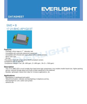
1. Product Overview
This document details the specifications for a compact, surface-mount blue LED designed for modern electronic applications. The device utilizes an InGaN (Indium Gallium Nitride) semiconductor chip to produce blue light with a typical dominant wavelength of 468 nm. Its primary advantages stem from its miniature SMD (Surface Mount Device) package, which enables significant reductions in PCB (Printed Circuit Board) footprint, allows for higher component packing density, and contributes to overall equipment miniaturization. The lightweight nature of the package further makes it suitable for portable and space-constrained applications.
1.1 Core Features and Compliance
The LED is supplied on 8mm tape wound onto 7-inch diameter reels, making it fully compatible with automated pick-and-place assembly equipment. It is designed for use with standard infrared and vapor phase reflow soldering processes. The device is a mono-color (blue) type. From a materials and environmental compliance perspective, it is lead-free (Pb-free), conforms to the RoHS (Restriction of Hazardous Substances) directive, is compliant with EU REACH regulations, and meets halogen-free standards with limits of Bromine (Br) < 900 ppm, Chlorine (Cl) < 900 ppm, and their sum (Br+Cl) < 1500 ppm.
1.2 Target Applications
The typical applications for this LED include backlighting for instrument panels, switches, and symbols. In telecommunications, it serves as an indicator or backlight in devices like telephones and fax machines. It is also suitable as a flat backlight source for LCDs and for general-purpose indicator use where a reliable, compact blue light source is required.
2. Technical Specifications Deep Dive
2.1 Absolute Maximum Ratings
These ratings define the limits beyond which permanent damage to the device may occur. They are not intended for continuous operation. The absolute maximum ratings are specified at an ambient temperature (Ta) of 25°C.
- Reverse Voltage (VR): 5 V. Exceeding this voltage in reverse bias can cause junction breakdown.
- Continuous Forward Current (IF): 20 mA.
- Peak Forward Current (IFP): 40 mA, permissible only under pulsed conditions with a duty cycle of 1/10 at 1 kHz.
- Power Dissipation (Pd): 75 mW. This is the maximum amount of power the device can dissipate as heat.
- Electrostatic Discharge (ESD) Human Body Model (HBM): 150 V. Proper ESD handling procedures must be followed.
- Operating Temperature Range (Topr): -40°C to +85°C.
- Storage Temperature Range (Tstg): -40°C to +90°C.
- Soldering Temperature (Tsol): For reflow soldering, a peak temperature of 260°C for a maximum of 10 seconds is specified. For hand soldering, the iron tip temperature should not exceed 350°C for a maximum of 3 seconds per terminal.
2.2 Electro-Optical Characteristics
These parameters define the device's performance under normal operating conditions, typically measured at Ta=25°C and a forward current (IF) of 20 mA, unless otherwise stated.
- Luminous Intensity (Iv): Ranges from a minimum of 45.0 mcd to a maximum of 112.0 mcd. The typical value is not specified in the table, falling within this bin-dependent range.
- Viewing Angle (2θ1/2): The half-intensity angle is typically 140 degrees, indicating a wide viewing cone.
- Peak Wavelength (λp): Typically 468 nm. This is the wavelength at which the spectral power distribution is maximum.
- Dominant Wavelength (λd): Ranges from 464.5 nm to 476.5 nm. This is the perceived color wavelength.
- Spectral Bandwidth (Δλ): Typically 25 nm, measured at half the maximum intensity (FWHM).
- Forward Voltage (VF): Ranges from 2.7 V (min) to 3.7 V (max), with a typical value of 3.3 V at IF=20mA.
- Reverse Current (IR): Maximum of 50 µA when a reverse voltage (VR) of 5V is applied. The device is not designed for operation in reverse bias.
Important Notes: Tolerances are specified as ±11% for luminous intensity, ±1 nm for dominant wavelength, and ±0.1V for forward voltage. The reverse voltage rating applies only to the IR test condition.
3. Binning System Explanation
To ensure consistency in production, LEDs are sorted into bins based on key performance parameters. This allows designers to select parts that meet specific brightness and color requirements.
3.1 Luminous Intensity Binning
Bins are defined by codes P1, P2, Q1, and Q2, each covering a specific range of luminous intensity measured in millicandelas (mcd) at IF=20mA.
- P1: 45.0 – 57.0 mcd
- P2: 57.0 – 72.0 mcd
- Q1: 72.0 – 90.0 mcd
- Q2: 90.0 – 112.0 mcd
3.2 Dominant Wavelength Binning
Wavelength bins are defined by codes A9 through A12, each covering a 3 nm range, ensuring tight color control.
- A9: 464.5 – 467.5 nm
- A10: 467.5 – 470.5 nm
- A11: 470.5 – 473.5 nm
- A12: 473.5 – 476.5 nm
4. Performance Curve Analysis
The datasheet provides several characteristic curves that are crucial for circuit design and thermal management.
4.1 Forward Current vs. Forward Voltage (I-V Curve)
This curve shows the nonlinear relationship between the current flowing through the LED and the voltage across it. The forward voltage (VF) increases with current. Designers use this curve to determine the necessary current-limiting resistor value for a given supply voltage to achieve the desired operating current (e.g., 20 mA). The typical VF of 3.3V is a key design parameter.
4.2 Relative Luminous Intensity vs. Forward Current
This graph illustrates how light output scales with drive current. While increasing current boosts brightness, it is not linear and is limited by the maximum current rating and thermal effects. Operating beyond the absolute maximum ratings will reduce lifespan and can cause failure.
4.3 Relative Luminous Intensity vs. Ambient Temperature
LED light output is temperature-dependent. This curve typically shows that luminous intensity decreases as the junction temperature rises. Understanding this derating is essential for applications operating at high ambient temperatures to ensure sufficient brightness is maintained.
4.4 Forward Current Derating Curve
This is a critical graph for reliability. It shows the maximum allowable continuous forward current as a function of the ambient temperature. As temperature increases, the maximum safe current decreases to prevent overheating and ensure long-term performance. Designers must ensure their operating point falls within this derated region.
4.5 Spectrum Distribution
The spectral graph plots the relative radiant power against wavelength. It confirms the blue color emission with a peak around 468 nm and a typical spectral bandwidth (Δλ) of 25 nm, indicating the color purity.
4.6 Radiation Diagram
This polar plot visualizes the spatial distribution of light intensity, confirming the wide 140-degree viewing angle. The intensity is normalized to its maximum value (typically at 0 degrees, perpendicular to the emitting surface).
5. Mechanical and Package Information
5.1 Package Dimensions
The LED is housed in a compact surface-mount package. Key dimensions (in mm, with a typical tolerance of ±0.1mm unless noted) include a body length of 2.0 mm, a width of 1.25 mm, and a height of 0.8 mm. The datasheet provides a detailed drawing showing pad layout, terminal spacing, and the location of the cathode identification mark, which is essential for correct PCB orientation during assembly.
5.2 Polarity Identification
Correct polarity is mandatory. The package features a distinct cathode mark. Connecting the device in reverse bias can damage it, as the maximum reverse voltage is only 5V.
6. Soldering and Assembly Guidelines
6.1 Reflow Soldering Profile
A lead-free reflow soldering temperature profile is specified. Key parameters include: a pre-heating stage between 150°C and 200°C for 60-120 seconds; a time above liquidus (217°C) of 60-150 seconds; a peak temperature not exceeding 260°C, held for a maximum of 10 seconds; and controlled ramp-up and cool-down rates (e.g., 3°C/sec max ramp-up, 6°C/sec max cool-down). Reflow should not be performed more than two times.
6.2 Hand Soldering Precautions
If hand soldering is necessary, extreme care is required. The soldering iron tip temperature must be below 350°C, and contact time per terminal must not exceed 3 seconds. A low-power iron (\u003c25W) is recommended. A cooling interval of at least 2 seconds should be allowed between soldering each terminal to prevent thermal shock.
6.3 Storage and Moisture Sensitivity
The LEDs are packaged in moisture-resistant bags with desiccant. The bag must not be opened until the components are ready for use. After opening, unused LEDs should be stored at ≤ 30°C and ≤ 60% Relative Humidity. The \"floor life\" after opening is 168 hours (7 days). If this time is exceeded or the desiccant indicator has changed color, a baking treatment at 60 ± 5°C for 24 hours is required before use to remove absorbed moisture and prevent \"popcorning\" during reflow.
7. Packaging and Ordering Information
7.1 Reel and Tape Specifications
The components are supplied in embossed carrier tape on 7-inch diameter reels. The tape width is 8 mm. Each reel contains 3000 pieces. Detailed dimensions for the reel, carrier tape pockets, and cover tape are provided to ensure compatibility with automated feeders.
7.2 Label Explanation
The packaging labels include several codes: CPN (Customer's Product Number), P/N (Product Number), QTY (Packing Quantity), CAT (Luminous Intensity Bin Code), HUE (Chromaticity/Dominant Wavelength Bin Code), REF (Forward Voltage Rank), and LOT No (Lot Number for traceability).
8. Application Notes and Design Considerations
8.1 Current Limiting is Mandatory
LEDs are current-driven devices. A series current-limiting resistor is absolutely essential in the circuit design. Without it, even a small increase in supply voltage can cause a large, potentially destructive increase in forward current due to the diode's exponential I-V characteristic.
8.2 Thermal Management
While the package is small, power dissipation (up to 75 mW) and the negative temperature coefficient of light output must be considered. For optimal performance and longevity, ensure adequate PCB copper area or thermal vias are used to dissipate heat, especially when operating at high ambient temperatures or near maximum current.
8.3 Optical Design
The wide 140-degree viewing angle makes this LED suitable for applications requiring broad illumination or visibility from multiple angles. For focused light, secondary optics (lenses) would be required. The water-clear resin allows for good light extraction.
9. Technical Comparison and Positioning
Compared to traditional through-hole LEDs, this SMD type offers significant advantages in assembly speed (compatible with pick-and-place), board space savings, and design flexibility. Within the SMD blue LED category, its key differentiators are its specific package size (2.0x1.25mm), typical 3.3V forward voltage, wide viewing angle, and defined binning structure for brightness and color consistency. The InGaN chip technology provides efficient blue emission.
10. Frequently Asked Questions (Based on Technical Parameters)
Q: What resistor value should I use with a 5V supply?
A: Using Ohm's Law (R = (Vsupply - Vf) / If) and typical values: R = (5V - 3.3V) / 0.020A = 85 Ohms. Use the nearest standard value (e.g., 82 or 91 Ohms) and consider the min/max Vf to ensure current stays within limits.
Q: Can I drive this LED at 30 mA for more brightness?
A: No. The absolute maximum continuous forward current is 20 mA. Exceeding this rating compromises reliability and may cause immediate or premature failure. Use the derating curve if operating at high temperature.
Q: The LED is very dim. What could be wrong?
A> First, check polarity. Second, verify the forward current using the voltage drop across the current-limiting resistor. Third, ensure the ambient temperature is not excessively high, as light output decreases with temperature.
Q: Do I need to bake the LEDs before soldering?
A> Only if the moisture-proof bag has been opened for more than 168 hours (7 days) or if the desiccant indicator shows moisture exposure. Follow the specified baking procedure (60°C for 24 hours).
11. Design and Usage Case Study
Scenario: Designing a status indicator panel with multiple blue LEDs.
A designer needs 10 uniform blue indicators on a control panel. They would:
1. Select LEDs from the same luminous intensity bin (e.g., Q1) and dominant wavelength bin (e.g., A10) to ensure visual consistency.
2. Design the PCB with a current-limiting resistor for each LED (calculated for a 3.3V typical Vf) to prevent current hogging.
3. Layout the board to provide some copper pour around the LED pads for minor heat dissipation.
4. Specify the assembly house to use the provided lead-free reflow profile and handle the moisture-sensitive devices according to the guidelines (store in sealed bags, use within floor life).
This approach ensures reliable operation, consistent appearance, and long-term performance.
12. Operating Principle
This LED operates on the principle of electroluminescence in a semiconductor p-n junction. The active region is made of InGaN. When a forward voltage exceeding the junction's built-in potential is applied, electrons and holes are injected into the active region where they recombine. This recombination process releases energy in the form of photons (light). The specific bandgap energy of the InGaN material determines the wavelength of the emitted photons, which in this case is in the blue region of the visible spectrum (~468 nm). The water-clear epoxy resin encapsulant protects the chip and helps shape the light output beam.
13. Technology Trends
Blue LEDs based on InGaN technology represent a mature and foundational technology in solid-state lighting. They are critical components not only for blue indicators but also as the pump source for generating white light in phosphor-converted white LEDs, which dominate the general lighting market. Ongoing development in this field focuses on increasing luminous efficacy (more light output per electrical watt), improving color consistency and stability over lifetime, enhancing reliability under high-temperature and high-current operation, and enabling even smaller package sizes for ultra-miniature applications. The drive for higher efficiency and lower cost per lumen continues to be a key industry trend.
LED Specification Terminology
Complete explanation of LED technical terms
Photoelectric Performance
| Term | Unit/Representation | Simple Explanation | Why Important |
|---|---|---|---|
| Luminous Efficacy | lm/W (lumens per watt) | Light output per watt of electricity, higher means more energy efficient. | Directly determines energy efficiency grade and electricity cost. |
| Luminous Flux | lm (lumens) | Total light emitted by source, commonly called "brightness". | Determines if the light is bright enough. |
| Viewing Angle | ° (degrees), e.g., 120° | Angle where light intensity drops to half, determines beam width. | Affects illumination range and uniformity. |
| CCT (Color Temperature) | K (Kelvin), e.g., 2700K/6500K | Warmth/coolness of light, lower values yellowish/warm, higher whitish/cool. | Determines lighting atmosphere and suitable scenarios. |
| CRI / Ra | Unitless, 0–100 | Ability to render object colors accurately, Ra≥80 is good. | Affects color authenticity, used in high-demand places like malls, museums. |
| SDCM | MacAdam ellipse steps, e.g., "5-step" | Color consistency metric, smaller steps mean more consistent color. | Ensures uniform color across same batch of LEDs. |
| Dominant Wavelength | nm (nanometers), e.g., 620nm (red) | Wavelength corresponding to color of colored LEDs. | Determines hue of red, yellow, green monochrome LEDs. |
| Spectral Distribution | Wavelength vs intensity curve | Shows intensity distribution across wavelengths. | Affects color rendering and quality. |
Electrical Parameters
| Term | Symbol | Simple Explanation | Design Considerations |
|---|---|---|---|
| Forward Voltage | Vf | Minimum voltage to turn on LED, like "starting threshold". | Driver voltage must be ≥Vf, voltages add up for series LEDs. |
| Forward Current | If | Current value for normal LED operation. | Usually constant current drive, current determines brightness & lifespan. |
| Max Pulse Current | Ifp | Peak current tolerable for short periods, used for dimming or flashing. | Pulse width & duty cycle must be strictly controlled to avoid damage. |
| Reverse Voltage | Vr | Max reverse voltage LED can withstand, beyond may cause breakdown. | Circuit must prevent reverse connection or voltage spikes. |
| Thermal Resistance | Rth (°C/W) | Resistance to heat transfer from chip to solder, lower is better. | High thermal resistance requires stronger heat dissipation. |
| ESD Immunity | V (HBM), e.g., 1000V | Ability to withstand electrostatic discharge, higher means less vulnerable. | Anti-static measures needed in production, especially for sensitive LEDs. |
Thermal Management & Reliability
| Term | Key Metric | Simple Explanation | Impact |
|---|---|---|---|
| Junction Temperature | Tj (°C) | Actual operating temperature inside LED chip. | Every 10°C reduction may double lifespan; too high causes light decay, color shift. |
| Lumen Depreciation | L70 / L80 (hours) | Time for brightness to drop to 70% or 80% of initial. | Directly defines LED "service life". |
| Lumen Maintenance | % (e.g., 70%) | Percentage of brightness retained after time. | Indicates brightness retention over long-term use. |
| Color Shift | Δu′v′ or MacAdam ellipse | Degree of color change during use. | Affects color consistency in lighting scenes. |
| Thermal Aging | Material degradation | Deterioration due to long-term high temperature. | May cause brightness drop, color change, or open-circuit failure. |
Packaging & Materials
| Term | Common Types | Simple Explanation | Features & Applications |
|---|---|---|---|
| Package Type | EMC, PPA, Ceramic | Housing material protecting chip, providing optical/thermal interface. | EMC: good heat resistance, low cost; Ceramic: better heat dissipation, longer life. |
| Chip Structure | Front, Flip Chip | Chip electrode arrangement. | Flip chip: better heat dissipation, higher efficacy, for high-power. |
| Phosphor Coating | YAG, Silicate, Nitride | Covers blue chip, converts some to yellow/red, mixes to white. | Different phosphors affect efficacy, CCT, and CRI. |
| Lens/Optics | Flat, Microlens, TIR | Optical structure on surface controlling light distribution. | Determines viewing angle and light distribution curve. |
Quality Control & Binning
| Term | Binning Content | Simple Explanation | Purpose |
|---|---|---|---|
| Luminous Flux Bin | Code e.g., 2G, 2H | Grouped by brightness, each group has min/max lumen values. | Ensures uniform brightness in same batch. |
| Voltage Bin | Code e.g., 6W, 6X | Grouped by forward voltage range. | Facilitates driver matching, improves system efficiency. |
| Color Bin | 5-step MacAdam ellipse | Grouped by color coordinates, ensuring tight range. | Guarantees color consistency, avoids uneven color within fixture. |
| CCT Bin | 2700K, 3000K etc. | Grouped by CCT, each has corresponding coordinate range. | Meets different scene CCT requirements. |
Testing & Certification
| Term | Standard/Test | Simple Explanation | Significance |
|---|---|---|---|
| LM-80 | Lumen maintenance test | Long-term lighting at constant temperature, recording brightness decay. | Used to estimate LED life (with TM-21). |
| TM-21 | Life estimation standard | Estimates life under actual conditions based on LM-80 data. | Provides scientific life prediction. |
| IESNA | Illuminating Engineering Society | Covers optical, electrical, thermal test methods. | Industry-recognized test basis. |
| RoHS / REACH | Environmental certification | Ensures no harmful substances (lead, mercury). | Market access requirement internationally. |
| ENERGY STAR / DLC | Energy efficiency certification | Energy efficiency and performance certification for lighting. | Used in government procurement, subsidy programs, enhances competitiveness. |