Table of Contents
- 1. Product Overview
- 2. Technical Parameters Deep Analysis
- 2.1 Photometric and Electrical Characteristics
- 2.2 Absolute Maximum Ratings and Thermal Management
- 3. Binning System Explanation
- 3.1 Luminous Flux Bins
- 3.2 Forward Voltage Bins
- 3.3 Color (Chromaticity) Bins
- 4. Performance Curve Analysis
- 4.1 IV Curve and Luminous Flux vs. Current
- 4.2 Temperature Dependence
- 4.3 Spectral Distribution
- 5. Mechanical and Package Information
- 6. Soldering and Assembly Guidelines
- 7. Packaging and Ordering Information
- 8. Application Recommendations
- 8.1 Typical Application Scenarios
- 8.2 Design Considerations
- 9. Technical Comparison and Differentiation
- 10. Frequently Asked Questions (FAQs)
- 10.1 What is the meaning of the MSL 2 rating?
- 10.2 How do I interpret the two different Thermal Resistance (Rth JS) values?
- 10.3 Can these LEDs be used in parallel without current balancing?
- 11. Practical Design Case Study
- 12. Operating Principle Introduction
- 13. Technology Trends
1. Product Overview
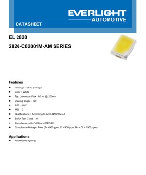
The 2820-C02001M-AM series is a high-performance, surface-mount device (SMD) LED designed primarily for demanding automotive lighting applications. It is built to meet stringent automotive-grade reliability standards, including AEC-Q102 qualification. The LED emits a cool white light and is offered in a compact 2820 package footprint, making it suitable for space-constrained designs where consistent, bright illumination is required.
Key advantages of this series include its robust construction for high-reliability environments, excellent luminous efficiency, and a wide 120-degree viewing angle that ensures broad and uniform light distribution. Its compliance with RoHS, REACH, and halogen-free directives further underscores its suitability for modern, environmentally conscious electronic assemblies.
2. Technical Parameters Deep Analysis
2.1 Photometric and Electrical Characteristics
The core performance is defined under a typical operating condition of 200 mA forward current (IF). At this current, the LED produces a typical luminous flux (IV) of 80 lumens (lm), with a minimum of 70 lm and a maximum of 100 lm. The forward voltage (VF) at 200 mA is typically 3.00 volts, ranging from 2.75V to 3.5V. This parameter is critical for driver circuit design and thermal management calculations.
The dominant chromaticity coordinates are specified at CIE x=0.3227 and CIE y=0.3351, defining a cool white point. The tolerance for these coordinates is ±0.005, ensuring color consistency within a batch. The device offers a wide viewing angle (φ) of 120 degrees, which is the angle where luminous intensity drops to half of its peak axial value.
2.2 Absolute Maximum Ratings and Thermal Management
To ensure long-term reliability, the device must not be operated beyond its Absolute Maximum Ratings. The maximum continuous forward current (IF) is 350 mA. The device can withstand a surge current (IFM) of 750 mA for pulses ≤ 10 µs with a low duty cycle. The maximum junction temperature (TJ) is 150°C.
Thermal management is crucial. The thermal resistance from the junction to the solder point (Rth JS) has two specified values: a real measurement of 20-22 K/W and an electrical measurement of 16 K/W max. The forward current derating curve clearly shows that the permissible continuous current must be reduced as the solder pad temperature (Ts) increases above 25°C. For example, at a Ts of 125°C, the maximum allowed IF is 350 mA, and it decreases linearly from there.
3. Binning System Explanation
The LEDs are sorted into bins to guarantee performance consistency for the end-user. Three key parameters are binned: Luminous Flux, Forward Voltage, and Chromaticity.
3.1 Luminous Flux Bins
Luminous flux bins are designated by codes like F7, F8, and F9. For instance, bin F7 covers LEDs with a luminous flux between 70 lm (min) and 80 lm (max) when measured at IF=200mA. This allows designers to select the brightness grade appropriate for their application.
3.2 Forward Voltage Bins
Forward voltage bins ensure electrical compatibility. Examples include bin 2730 (VF: 2.75V - 3.00V) and bin 3032 (VF: 3.00V - 3.25V). Matching LEDs from the same voltage bin can help achieve uniform current distribution in parallel configurations.
3.3 Color (Chromaticity) Bins
The provided chromaticity diagram shows the structure for cool white bins, such as 56M, 58M, 61M, and 63M. Each bin is defined by a quadrilateral area on the CIE 1931 chromaticity chart, specified by four sets of (x, y) coordinates. This precise binning ensures tight color control, which is vital in automotive lighting where color matching across multiple LEDs is often required.
4. Performance Curve Analysis
4.1 IV Curve and Luminous Flux vs. Current
The Forward Current vs. Forward Voltage graph shows a typical diode exponential relationship. At 200 mA, the VF is centered around 3.0V. The Relative Luminous Flux vs. Forward Current graph indicates that light output increases sub-linearly with current. While increasing current boosts output, it also increases power dissipation and junction temperature, which can affect longevity and color stability.
4.2 Temperature Dependence
The Relative Luminous Flux vs. Junction Temperature graph is critical for thermal design. Luminous output decreases as junction temperature rises. At 100°C, the relative flux is approximately 85% of its value at 25°C. This underscores the importance of effective heat sinking.
The Chromaticity Coordinates Shift vs. Junction Temperature graph shows minimal shift (Δx, Δy within ±0.01) across the -50°C to +125°C range, indicating good color stability with temperature. The Forward Voltage has a negative temperature coefficient, decreasing by about 2 mV/°C.
4.3 Spectral Distribution
The Relative Spectral Distribution graph shows a peak in the blue wavelength region (around 450-455 nm) typical for a phosphor-converted white LED, with a broad secondary peak in the yellow region from the phosphor, combining to produce white light.
5. Mechanical and Package Information
The LED uses a standard 2820 SMD package. The mechanical drawing specifies the physical dimensions in millimeters. Key features include the anode and cathode pad locations and the overall package height. The recommended soldering pad layout is provided to ensure proper mechanical attachment, electrical connection, and optimal thermal transfer from the LED's thermal pad to the PCB. Adhering to this land pattern is essential for reliability, especially under thermal cycling conditions experienced in automotive environments.
6. Soldering and Assembly Guidelines
The device is rated for reflow soldering with a peak temperature of 260°C for a maximum of 30 seconds, as per the IPC/JEDEC J-STD-020 profile. The Moisture Sensitivity Level (MSL) is 2, meaning the components must be baked if exposed to ambient conditions for longer than one year before use. Following the recommended reflow profile and handling precautions is mandatory to prevent package cracking or solder joint defects.
7. Packaging and Ordering Information
The LEDs are supplied on tape and reel for automated assembly. The packaging information details the reel dimensions, tape width, pocket spacing, and orientation of the components on the tape. The part number structure (e.g., 2820-C02001M-AM) encodes key attributes such as the package size (2820), color/chip type (C02001M), and series designation (AM). Ordering involves specifying the required bins for luminous flux, forward voltage, and chromaticity.
8. Application Recommendations
8.1 Typical Application Scenarios
The primary application is automotive lighting. This includes interior lighting (dome lights, map lights, ambient lighting), exterior signaling (center high-mount stop lights - CHMSL), and potentially some auxiliary lighting functions. Its AEC-Q102 qualification and sulfur resistance (Class A1) make it suitable for the harsh under-hood or exterior vehicle environment.
8.2 Design Considerations
Driver Circuit: A constant-current driver is essential to maintain stable light output and prevent thermal runaway. The driver must be designed to accommodate the forward voltage bin range and provide adequate current limiting up to 350 mA.
Thermal Design: Effective thermal management is non-negotiable. The PCB should use thermal vias under the LED's thermal pad connected to a large copper plane or an external heatsink to minimize the temperature rise at the solder point (Ts). Always refer to the forward current derating curve.
Optical Design: The 120-degree viewing angle provides wide coverage. For focused applications, secondary optics (lenses, reflectors) will be required. The mechanical drawing provides the necessary dimensions for designing such optics.
ESD Protection: While the LED has a robust ESD rating of 8 kV (HBM), standard ESD handling precautions during assembly are still recommended.
9. Technical Comparison and Differentiation
Compared to generic commercial-grade LEDs, the key differentiators of this series are its automotive-grade reliability certifications (AEC-Q102), explicit sulfur gas resistance testing (Class A1), and extended operating temperature range (-40°C to +125°C). The detailed binning structure for color and flux provides a level of consistency required for automotive applications where multiple LEDs are used in a single assembly. The combination of good luminous efficacy (80 lm at 200mA equates to ~133 lm/W considering ~0.6W input) and a wide viewing angle in a compact package offers a balanced solution for space and performance-critical designs.
10. Frequently Asked Questions (FAQs)
10.1 What is the meaning of the MSL 2 rating?
MSL 2 (Moisture Sensitivity Level 2) indicates that the packaged LED can be exposed to factory floor ambient conditions (
10.2 How do I interpret the two different Thermal Resistance (Rth JS) values?
The datasheet lists a "Real" Rth JS of 20-22 K/W and an "Electrical" Rth JS of 16 K/W max. The "real" value is typically measured using a physical temperature sensor and is considered more accurate for thermal modeling. The "electrical" method uses the temperature-sensitive forward voltage as a proxy for junction temperature. For conservative thermal design, using the higher "real" value (22 K/W) is recommended to ensure a sufficient safety margin.
10.3 Can these LEDs be used in parallel without current balancing?
Direct parallel connection is generally not recommended without additional measures. Due to natural variations in forward voltage (even within a bin), LEDs in parallel will not share current equally. The LED with the slightly lower VF will draw more current, potentially leading to overheating and accelerated degradation. Using a separate current-limiting resistor for each LED or dedicated multi-channel constant-current drivers is the preferred method for driving multiple LEDs.
11. Practical Design Case Study
Scenario: Designing an automotive CHMSL (Center High-Mount Stop Light) module using 10 pieces of the 2820-C02001M-AM LED.
Design Steps:
- Electrical Design: Target operating current per LED: 200 mA for optimal efficiency and lifetime. Total current: 2.0A. Select a constant-current LED driver IC capable of delivering 2.0A, with an input voltage range covering the automotive battery system (9V-16V nominal, with load-dump transients). Choose LEDs from the same forward voltage bin (e.g., 3032) to minimize current imbalance if a single-channel driver is used with all LEDs in series.
- Thermal Design: Estimate total power dissipation: 10 LEDs * (3.0V * 0.2A) = 6.0W. Using the conservative Rth JS of 22 K/W and assuming a target maximum junction temperature (Tj) of 110°C (below the 150°C max), calculate the required maximum solder point temperature: Ts_max = Tj_max - (Power_per_LED * Rth JS) = 110 - (0.6 * 22) = 96.8°C. The PCB must be designed with a thermal pad and sufficient copper area/thermal vias to keep Ts below this value in the expected ambient environment (e.g., inside a hot car trunk).
- Optical/Mechanical Design: The 120-degree viewing angle may be sufficient for a CHMSL, but a reflector or lens may be added to meet specific photometric intensity requirements (e.g., SAE standards). The mechanical drawing provides the footprint for PCB layout and the dimensions for designing a holder or lens clip.
- Component Selection: Order all 10 LEDs from the same luminous flux bin (e.g., F8) and the same chromaticity bin (e.g., 58M) to ensure uniform brightness and color across the light bar.
12. Operating Principle Introduction
This LED is a phosphor-converted white LED. At its core is a semiconductor chip, typically made of indium gallium nitride (InGaN), that emits blue light when forward biased (electrical current flows through it). This blue light is partially absorbed by a layer of cerium-doped yttrium aluminum garnet (YAG:Ce) phosphor coating deposited on or near the chip. The phosphor absorbs some of the blue photons and re-emits light across a broad spectrum centered in the yellow region. The combination of the remaining unabsorbed blue light and the emitted yellow light is perceived by the human eye as white light. The exact shade of white (cool, neutral, warm) is determined by the ratio of blue to yellow light, which is controlled by the phosphor composition and thickness.
13. Technology Trends
The trend in automotive LED lighting continues towards higher luminous efficacy (more lumens per watt), enabling brighter lights or lower power consumption and thermal load. There is also a strong drive for improved color rendering index (CRI) and color consistency, especially for interior ambient lighting where user experience is key. Miniaturization persists, with packages becoming smaller while maintaining or increasing light output. Furthermore, integration is a growing trend, with LED packages incorporating driver ICs, sensors, or communication interfaces for smart lighting systems. The emphasis on reliability and qualification for harsh environments (high temperature, humidity, vibration, chemical exposure) remains paramount in the automotive sector.
LED Specification Terminology
Complete explanation of LED technical terms
Photoelectric Performance
| Term | Unit/Representation | Simple Explanation | Why Important |
|---|---|---|---|
| Luminous Efficacy | lm/W (lumens per watt) | Light output per watt of electricity, higher means more energy efficient. | Directly determines energy efficiency grade and electricity cost. |
| Luminous Flux | lm (lumens) | Total light emitted by source, commonly called "brightness". | Determines if the light is bright enough. |
| Viewing Angle | ° (degrees), e.g., 120° | Angle where light intensity drops to half, determines beam width. | Affects illumination range and uniformity. |
| CCT (Color Temperature) | K (Kelvin), e.g., 2700K/6500K | Warmth/coolness of light, lower values yellowish/warm, higher whitish/cool. | Determines lighting atmosphere and suitable scenarios. |
| CRI / Ra | Unitless, 0–100 | Ability to render object colors accurately, Ra≥80 is good. | Affects color authenticity, used in high-demand places like malls, museums. |
| SDCM | MacAdam ellipse steps, e.g., "5-step" | Color consistency metric, smaller steps mean more consistent color. | Ensures uniform color across same batch of LEDs. |
| Dominant Wavelength | nm (nanometers), e.g., 620nm (red) | Wavelength corresponding to color of colored LEDs. | Determines hue of red, yellow, green monochrome LEDs. |
| Spectral Distribution | Wavelength vs intensity curve | Shows intensity distribution across wavelengths. | Affects color rendering and quality. |
Electrical Parameters
| Term | Symbol | Simple Explanation | Design Considerations |
|---|---|---|---|
| Forward Voltage | Vf | Minimum voltage to turn on LED, like "starting threshold". | Driver voltage must be ≥Vf, voltages add up for series LEDs. |
| Forward Current | If | Current value for normal LED operation. | Usually constant current drive, current determines brightness & lifespan. |
| Max Pulse Current | Ifp | Peak current tolerable for short periods, used for dimming or flashing. | Pulse width & duty cycle must be strictly controlled to avoid damage. |
| Reverse Voltage | Vr | Max reverse voltage LED can withstand, beyond may cause breakdown. | Circuit must prevent reverse connection or voltage spikes. |
| Thermal Resistance | Rth (°C/W) | Resistance to heat transfer from chip to solder, lower is better. | High thermal resistance requires stronger heat dissipation. |
| ESD Immunity | V (HBM), e.g., 1000V | Ability to withstand electrostatic discharge, higher means less vulnerable. | Anti-static measures needed in production, especially for sensitive LEDs. |
Thermal Management & Reliability
| Term | Key Metric | Simple Explanation | Impact |
|---|---|---|---|
| Junction Temperature | Tj (°C) | Actual operating temperature inside LED chip. | Every 10°C reduction may double lifespan; too high causes light decay, color shift. |
| Lumen Depreciation | L70 / L80 (hours) | Time for brightness to drop to 70% or 80% of initial. | Directly defines LED "service life". |
| Lumen Maintenance | % (e.g., 70%) | Percentage of brightness retained after time. | Indicates brightness retention over long-term use. |
| Color Shift | Δu′v′ or MacAdam ellipse | Degree of color change during use. | Affects color consistency in lighting scenes. |
| Thermal Aging | Material degradation | Deterioration due to long-term high temperature. | May cause brightness drop, color change, or open-circuit failure. |
Packaging & Materials
| Term | Common Types | Simple Explanation | Features & Applications |
|---|---|---|---|
| Package Type | EMC, PPA, Ceramic | Housing material protecting chip, providing optical/thermal interface. | EMC: good heat resistance, low cost; Ceramic: better heat dissipation, longer life. |
| Chip Structure | Front, Flip Chip | Chip electrode arrangement. | Flip chip: better heat dissipation, higher efficacy, for high-power. |
| Phosphor Coating | YAG, Silicate, Nitride | Covers blue chip, converts some to yellow/red, mixes to white. | Different phosphors affect efficacy, CCT, and CRI. |
| Lens/Optics | Flat, Microlens, TIR | Optical structure on surface controlling light distribution. | Determines viewing angle and light distribution curve. |
Quality Control & Binning
| Term | Binning Content | Simple Explanation | Purpose |
|---|---|---|---|
| Luminous Flux Bin | Code e.g., 2G, 2H | Grouped by brightness, each group has min/max lumen values. | Ensures uniform brightness in same batch. |
| Voltage Bin | Code e.g., 6W, 6X | Grouped by forward voltage range. | Facilitates driver matching, improves system efficiency. |
| Color Bin | 5-step MacAdam ellipse | Grouped by color coordinates, ensuring tight range. | Guarantees color consistency, avoids uneven color within fixture. |
| CCT Bin | 2700K, 3000K etc. | Grouped by CCT, each has corresponding coordinate range. | Meets different scene CCT requirements. |
Testing & Certification
| Term | Standard/Test | Simple Explanation | Significance |
|---|---|---|---|
| LM-80 | Lumen maintenance test | Long-term lighting at constant temperature, recording brightness decay. | Used to estimate LED life (with TM-21). |
| TM-21 | Life estimation standard | Estimates life under actual conditions based on LM-80 data. | Provides scientific life prediction. |
| IESNA | Illuminating Engineering Society | Covers optical, electrical, thermal test methods. | Industry-recognized test basis. |
| RoHS / REACH | Environmental certification | Ensures no harmful substances (lead, mercury). | Market access requirement internationally. |
| ENERGY STAR / DLC | Energy efficiency certification | Energy efficiency and performance certification for lighting. | Used in government procurement, subsidy programs, enhances competitiveness. |