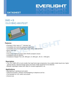
1. Product Overview
The 15-21/BHC-AN1P2/2T is a compact, surface-mount blue LED designed for modern electronic applications requiring high-density component placement. Its primary advantage lies in its significantly reduced footprint compared to traditional lead-frame LEDs, enabling smaller printed circuit board (PCB) designs and more compact end products. The device is constructed using InGaN (Indium Gallium Nitride) chip technology, encapsulated in a water-clear resin, which emits light in the blue spectrum. It is fully compliant with RoHS, REACH, and halogen-free directives, making it suitable for environmentally conscious manufacturing processes.
1.1 Core Advantages
The key benefits of this LED include its miniature size (2.0mm x 1.25mm x 0.8mm), which directly contributes to reduced storage space and higher packing density on PCBs. Its lightweight nature makes it ideal for portable and miniature applications. The component is supplied on 8mm tape mounted on 7-inch diameter reels, ensuring compatibility with high-speed automated pick-and-place assembly equipment. Furthermore, it is designed to withstand standard infrared and vapor phase reflow soldering processes, facilitating efficient mass production.
1.2 Target Applications
This LED is versatile and finds use in various illumination and indication roles. Common applications include backlighting for instrument panel dashboards, switches, and keypads. In telecommunications equipment, it serves as status indicators and backlights for devices like telephones and fax machines. It is also suitable for providing flat backlighting for liquid crystal displays (LCDs) and general-purpose indicator functions where a reliable, compact blue light source is required.
2. Technical Parameter Deep Dive
This section provides a detailed, objective analysis of the device's key electrical, optical, and thermal specifications as defined in the Absolute Maximum Ratings and Electro-Optical Characteristics tables.
2.1 Absolute Maximum Ratings
The Absolute Maximum Ratings define the stress limits beyond which permanent damage to the device may occur. These are not operating conditions. The maximum reverse voltage (V_R) is 5V. Exceeding this can cause junction breakdown. The continuous forward current (I_F) is rated at 25mA. For pulsed operation, a peak forward current (I_FP) of 100mA is permissible under a duty cycle of 1/10 at 1kHz. The maximum power dissipation (P_d) is 95mW, calculated as the product of forward voltage and current. The device can withstand an electrostatic discharge (ESD) of 150V per the Human Body Model (HBM). The operating temperature range (T_opr) is from -40°C to +85°C, and the storage temperature (T_stg) extends slightly to -40°C to +90°C. The soldering temperature profile is critical: for reflow, a peak of 260°C for a maximum of 10 seconds is specified; for hand soldering, the iron tip temperature must not exceed 350°C for 3 seconds per terminal.
2.2 Electro-Optical Characteristics
These parameters are measured at a standard test condition of 25°C ambient temperature and a forward current of 20mA. The luminous intensity (I_v) has a typical value within a wide range defined by the binning system, with a minimum of 28.5 mcd and a maximum of 72.0 mcd. The viewing angle (2θ1/2) is typically 130 degrees, indicating a wide, diffuse emission pattern. The peak wavelength (λ_p) is typically 468 nm, and the dominant wavelength (λ_d) ranges from 464.5 nm to 476.5 nm, defining the perceived blue color. The spectral bandwidth (Δλ) is typically 25 nm. The forward voltage (V_F) ranges from 2.7V (min) to 3.7V (max), with a typical value of 3.3V at 20mA. The reverse current (I_R) is very low, with a maximum of 50 µA at the full 5V reverse bias.
3. Binning System Explanation
To ensure consistency in production, LEDs are sorted into performance bins. This allows designers to select parts that meet specific brightness and color requirements.
3.1 Luminous Intensity Binning
The luminous output is categorized into four distinct bins: N1 (28.5-36.0 mcd), N2 (36.0-45.0 mcd), P1 (45.0-57.0 mcd), and P2 (57.0-72.0 mcd). A tolerance of ±11% applies within each bin. Designers must account for this variation when designing for minimum brightness levels in their application.
3.2 Dominant Wavelength Binning
The color (dominant wavelength) is also binned to control hue variation. The bins are A9 (464.5-467.5 nm), A10 (467.5-470.5 nm), A11 (470.5-473.5 nm), and A12 (473.5-476.5 nm). A tolerance of ±1nm is specified. This binning is crucial for applications where color consistency across multiple LEDs is important, such as in backlighting arrays.
4. Performance Curve Analysis
While the PDF indicates a section for typical electro-optical characteristic curves, specific graphical data (e.g., I-V curves, intensity vs. current, wavelength vs. temperature) is not provided in the extracted text. In a complete datasheet, these curves are essential for understanding device behavior under non-standard conditions. Designers typically rely on such curves to predict performance at different operating currents and ambient temperatures, which directly affects luminous output, forward voltage, and long-term reliability.
5. Mechanical and Package Information
5.1 Package Dimensions
The LED conforms to the 15-21 SMD package standard. The key dimensions are approximately 2.0mm in length, 1.25mm in width, and 0.8mm in height. The package drawing specifies the location and size of the solder pads (typically 0.6mm x 0.9mm), the gap between them, and the overall tolerances (generally ±0.1mm unless otherwise noted). This precise dimensional data is critical for creating an accurate PCB land pattern (footprint) to ensure proper soldering and alignment.
5.2 Polarity Identification
The cathode (negative terminal) is typically marked on the device, often by a small notch, a green dot, or a chamfered corner on the package. The provided dimension drawing should clearly indicate this marking. Correct polarity orientation during assembly is mandatory for the device to function.
6. Soldering and Assembly Guidelines
Proper handling and soldering are critical to maintaining device integrity and performance.
6.1 Reflow Soldering Parameters
A lead-free reflow profile is specified. The pre-heating zone should ramp from 150°C to 200°C over 60-120 seconds. The time above the solder liquidus temperature (217°C) should be 60-150 seconds. The peak temperature must not exceed 260°C, and the time at this peak should be a maximum of 10 seconds. The maximum ramp-up rate is 6°C/sec, and the maximum ramp-down rate is 3°C/sec. Reflow soldering should not be performed more than two times on the same device.
6.2 Storage and Moisture Sensitivity
The LEDs are packaged in moisture-resistant barrier bags with desiccant. The bag must not be opened until the components are ready for use. Before opening, storage conditions should be ≤30°C and ≤90% RH. After opening, the "floor life" is 1 year under conditions of ≤30°C and ≤60% RH. If the desiccant indicator shows saturation or the storage time is exceeded, a baking treatment at 60±5°C for 24 hours is required before reflow to prevent "popcorning" damage during soldering.
6.3 Hand Soldering and Repair Precautions
If hand soldering is necessary, extreme care is advised. A soldering iron with a tip temperature below 350°C and a power rating below 25W should be used. Contact time per terminal must not exceed 3 seconds. A minimum interval of 2 seconds should be left between soldering each terminal. Repair after initial soldering is strongly discouraged. If unavoidable, a specialized double-head soldering iron should be used to simultaneously heat both terminals and avoid mechanical stress on the package.
7. Packaging and Ordering Information
7.1 Packaging Specifications
The product is supplied on embossed carrier tape with dimensions tailored to the 15-21 package. The tape is wound onto a standard 7-inch (178mm) diameter reel. Each reel contains 2000 pieces. The reel, tape, and cover tape dimensions are provided in the datasheet drawings to ensure compatibility with automated feeders.
7.2 Label Explanation
The reel label contains several key codes: P/N (Product Number: 15-21/BHC-AN1P2/2T), QTY (Packing Quantity: 2000), CAT (Luminous Intensity Rank, e.g., N1, P2), HUE (Chromaticity/Dominant Wavelength Rank, e.g., A10, A12), REF (Forward Voltage Rank), and LOT No (Traceable Lot Number). The CPN field is for a customer's internal part number.
8. Application Design Suggestions
8.1 Current Limiting Requirement
LEDs are current-driven devices. A series current-limiting resistor is absolutely mandatory in the circuit design to prevent thermal runaway and destruction. The datasheet shows that a slight increase in forward voltage can cause a large increase in current. The resistor value should be calculated based on the supply voltage (V_supply), the LED's typical forward voltage (V_F, e.g., 3.3V), and the desired operating current (I_F, must be ≤25mA continuous). The formula is R = (V_supply - V_F) / I_F.
8.2 Thermal Management Considerations
Although small, the LED dissipates heat (up to 95mW). For reliable long-term operation, especially at high ambient temperatures or near the maximum current, adequate PCB copper area (thermal relief pads) should be used to conduct heat away from the solder joints and the LED die itself. Operating at lower currents than the maximum rating significantly improves lifetime and reliability.
9. Technical Comparison and Differentiation
The primary differentiation of the 15-21 package LED compared to larger SMD LEDs (e.g., 3528, 5050) or through-hole LEDs is its ultra-compact size, enabling design miniaturization. Compared to other miniaturized LEDs, its key advantages include a wide 130-degree viewing angle for even illumination, compliance with stringent environmental regulations (RoHS, Halogen-Free), and robust specifications for automated reflow assembly. The detailed binning system provides designers with predictable performance parameters for color and brightness.
10. Frequently Asked Questions (Based on Technical Parameters)
Q: Can I drive this LED directly from a 5V supply without a resistor?
A: No. This will almost certainly destroy the LED. You must use a series current-limiting resistor as described in section 8.1.
Q: What is the difference between Peak Wavelength and Dominant Wavelength?
A: Peak wavelength (λ_p) is the wavelength at which the emission spectrum has its highest intensity. Dominant wavelength (λ_d) is the single wavelength of monochromatic light that matches the perceived color of the LED. λ_d is more relevant for color specification.
Q: How do I interpret the bin codes (e.g., P2 A11) when ordering?
A> The bin code specifies the guaranteed performance range. "P2" means the luminous intensity is between 57.0 and 72.0 mcd. "A11" means the dominant wavelength is between 470.5 and 473.5 nm. You should select bins that meet your application's minimum brightness and color consistency requirements.
Q: Is this LED suitable for automotive dashboard lighting?
A: While it is listed for dashboard backlighting, the "Application Restrictions" section explicitly states that high-reliability applications like automotive safety systems may require different products. For such critical applications, consultation with the manufacturer and potentially using an AEC-Q102 qualified component is necessary.
11. Design and Usage Case Study
Scenario: Designing a compact status indicator panel for a portable medical device.
The design requires four blue status LEDs in a tight space. The 15-21 package is selected for its small size. The designer chooses the P1 brightness bin (45-57 mcd) to ensure adequate visibility. The A10 wavelength bin (467.5-470.5 nm) is selected for color consistency. The circuit is powered by a 3.3V rail. Using the typical V_F of 3.3V at 20mA, a very small series resistor (e.g., 0-1 Ohm) or a constant current driver set to 18mA (for margin) would be used. The PCB layout includes thermal pads connected to a ground plane for heat dissipation. The assembly follows the specified reflow profile, and the moisture-sensitive devices are used within the prescribed floor life after bag opening.
12. Operating Principle
This LED operates on the principle of electroluminescence in a semiconductor p-n junction. The active region is made of InGaN. When a forward voltage exceeding the junction's built-in potential is applied, electrons and holes are injected into the active region. When these charge carriers recombine, they release energy in the form of photons (light). The specific composition of the InGaN alloy determines the bandgap energy, which in turn dictates the wavelength (color) of the emitted light, in this case, blue. The water-clear resin encapsulation protects the semiconductor die and acts as a lens to shape the light output beam.
13. Technology Trends
The development of SMD LEDs like the 15-21 package is driven by the ongoing trend towards miniaturization and increased functionality in electronic devices. Key trends in this sector include continued reduction in package size while maintaining or increasing light output (higher efficacy), improved color rendering and consistency through advanced binning and chip technology, and enhanced reliability for operation in harsh environments (higher temperature, humidity). Furthermore, integration with intelligent drivers and the development of micro-LED arrays for display applications represent significant future directions in solid-state lighting technology.
LED Specification Terminology
Complete explanation of LED technical terms
Photoelectric Performance
| Term | Unit/Representation | Simple Explanation | Why Important |
|---|---|---|---|
| Luminous Efficacy | lm/W (lumens per watt) | Light output per watt of electricity, higher means more energy efficient. | Directly determines energy efficiency grade and electricity cost. |
| Luminous Flux | lm (lumens) | Total light emitted by source, commonly called "brightness". | Determines if the light is bright enough. |
| Viewing Angle | ° (degrees), e.g., 120° | Angle where light intensity drops to half, determines beam width. | Affects illumination range and uniformity. |
| CCT (Color Temperature) | K (Kelvin), e.g., 2700K/6500K | Warmth/coolness of light, lower values yellowish/warm, higher whitish/cool. | Determines lighting atmosphere and suitable scenarios. |
| CRI / Ra | Unitless, 0–100 | Ability to render object colors accurately, Ra≥80 is good. | Affects color authenticity, used in high-demand places like malls, museums. |
| SDCM | MacAdam ellipse steps, e.g., "5-step" | Color consistency metric, smaller steps mean more consistent color. | Ensures uniform color across same batch of LEDs. |
| Dominant Wavelength | nm (nanometers), e.g., 620nm (red) | Wavelength corresponding to color of colored LEDs. | Determines hue of red, yellow, green monochrome LEDs. |
| Spectral Distribution | Wavelength vs intensity curve | Shows intensity distribution across wavelengths. | Affects color rendering and quality. |
Electrical Parameters
| Term | Symbol | Simple Explanation | Design Considerations |
|---|---|---|---|
| Forward Voltage | Vf | Minimum voltage to turn on LED, like "starting threshold". | Driver voltage must be ≥Vf, voltages add up for series LEDs. |
| Forward Current | If | Current value for normal LED operation. | Usually constant current drive, current determines brightness & lifespan. |
| Max Pulse Current | Ifp | Peak current tolerable for short periods, used for dimming or flashing. | Pulse width & duty cycle must be strictly controlled to avoid damage. |
| Reverse Voltage | Vr | Max reverse voltage LED can withstand, beyond may cause breakdown. | Circuit must prevent reverse connection or voltage spikes. |
| Thermal Resistance | Rth (°C/W) | Resistance to heat transfer from chip to solder, lower is better. | High thermal resistance requires stronger heat dissipation. |
| ESD Immunity | V (HBM), e.g., 1000V | Ability to withstand electrostatic discharge, higher means less vulnerable. | Anti-static measures needed in production, especially for sensitive LEDs. |
Thermal Management & Reliability
| Term | Key Metric | Simple Explanation | Impact |
|---|---|---|---|
| Junction Temperature | Tj (°C) | Actual operating temperature inside LED chip. | Every 10°C reduction may double lifespan; too high causes light decay, color shift. |
| Lumen Depreciation | L70 / L80 (hours) | Time for brightness to drop to 70% or 80% of initial. | Directly defines LED "service life". |
| Lumen Maintenance | % (e.g., 70%) | Percentage of brightness retained after time. | Indicates brightness retention over long-term use. |
| Color Shift | Δu′v′ or MacAdam ellipse | Degree of color change during use. | Affects color consistency in lighting scenes. |
| Thermal Aging | Material degradation | Deterioration due to long-term high temperature. | May cause brightness drop, color change, or open-circuit failure. |
Packaging & Materials
| Term | Common Types | Simple Explanation | Features & Applications |
|---|---|---|---|
| Package Type | EMC, PPA, Ceramic | Housing material protecting chip, providing optical/thermal interface. | EMC: good heat resistance, low cost; Ceramic: better heat dissipation, longer life. |
| Chip Structure | Front, Flip Chip | Chip electrode arrangement. | Flip chip: better heat dissipation, higher efficacy, for high-power. |
| Phosphor Coating | YAG, Silicate, Nitride | Covers blue chip, converts some to yellow/red, mixes to white. | Different phosphors affect efficacy, CCT, and CRI. |
| Lens/Optics | Flat, Microlens, TIR | Optical structure on surface controlling light distribution. | Determines viewing angle and light distribution curve. |
Quality Control & Binning
| Term | Binning Content | Simple Explanation | Purpose |
|---|---|---|---|
| Luminous Flux Bin | Code e.g., 2G, 2H | Grouped by brightness, each group has min/max lumen values. | Ensures uniform brightness in same batch. |
| Voltage Bin | Code e.g., 6W, 6X | Grouped by forward voltage range. | Facilitates driver matching, improves system efficiency. |
| Color Bin | 5-step MacAdam ellipse | Grouped by color coordinates, ensuring tight range. | Guarantees color consistency, avoids uneven color within fixture. |
| CCT Bin | 2700K, 3000K etc. | Grouped by CCT, each has corresponding coordinate range. | Meets different scene CCT requirements. |
Testing & Certification
| Term | Standard/Test | Simple Explanation | Significance |
|---|---|---|---|
| LM-80 | Lumen maintenance test | Long-term lighting at constant temperature, recording brightness decay. | Used to estimate LED life (with TM-21). |
| TM-21 | Life estimation standard | Estimates life under actual conditions based on LM-80 data. | Provides scientific life prediction. |
| IESNA | Illuminating Engineering Society | Covers optical, electrical, thermal test methods. | Industry-recognized test basis. |
| RoHS / REACH | Environmental certification | Ensures no harmful substances (lead, mercury). | Market access requirement internationally. |
| ENERGY STAR / DLC | Energy efficiency certification | Energy efficiency and performance certification for lighting. | Used in government procurement, subsidy programs, enhances competitiveness. |