Table of Contents
- 1. Product Overview
- 1.1 Core Advantages and Product Positioning
- 1.2 Compliance and Environmental Specifications
- 2. Technical Parameters: In-Depth Objective Interpretation
- 2.1 Absolute Maximum Ratings
- 2.2 Electro-Optical Characteristics
- 3. Binning System Explanation
- 3.1 Luminous Intensity Binning
- 3.2 Dominant Wavelength Binning
- 3.3 Forward Voltage Binning
- 4. Performance Curve Analysis
- 5. Mechanical and Package Information
- 5.1 Package Dimensions
- 5.2 Polarity Identification
- 6. Soldering and Assembly Guidelines
- 6.1 Reflow Soldering Profile (Pb-free)
- 6.2 Hand Soldering
- 6.3 Storage and Moisture Sensitivity
- 6.4 Precautions for Use
- 7. Packaging and Ordering Information
- 7.1 Tape and Reel Specifications
- 7.2 Label Explanation
- 8. Application Suggestions and Design Considerations
- 8.1 Typical Application Scenarios
- 8.2 Circuit Design Considerations
- 8.3 Application Restrictions
- 9. Technical Comparison and Differentiation
- 10. Frequently Asked Questions (Based on Technical Parameters)
- 11. Practical Design and Usage Case
- 12. Operating Principle Introduction
- 13. Technology Trends and Context
1. Product Overview
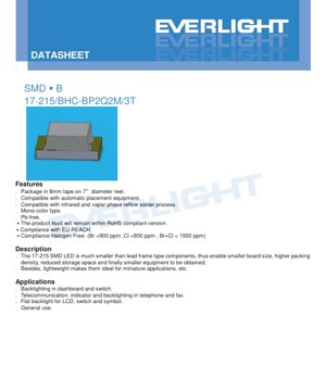
The 17-215/BHC-BP2Q2M/3T is a surface-mount device (SMD) light-emitting diode (LED) utilizing an InGaN (Indium Gallium Nitride) semiconductor chip to produce blue light. This component is designed for modern, automated electronics manufacturing processes, offering a compact footprint that enables higher board density and miniaturization of end equipment compared to traditional lead-frame LEDs.
1.1 Core Advantages and Product Positioning
The primary advantages of this LED stem from its SMD package. Its significantly smaller size allows for reduced printed circuit board (PCB) area, lower storage space requirements, and ultimately contributes to the development of smaller and lighter electronic devices. The lightweight nature of the package makes it particularly suitable for miniature and portable applications. The product is positioned as a general-purpose indicator and backlighting solution, compliant with contemporary environmental and manufacturing standards.
1.2 Compliance and Environmental Specifications
This component adheres to several key industry standards. It is manufactured as a Pb-free (lead-free) product. The materials used comply with the EU REACH regulation. Furthermore, it meets halogen-free requirements, with Bromine (Br) and Chlorine (Cl) content each below 900 ppm, and their combined total below 1500 ppm. The product is also designed to remain within the specifications of the RoHS (Restriction of Hazardous Substances) directive.
2. Technical Parameters: In-Depth Objective Interpretation
The following sections provide a detailed, objective analysis of the device's electrical, optical, and thermal characteristics as defined in the datasheet. All parameters are specified at an ambient temperature (Ta) of 25°C unless otherwise noted.
2.1 Absolute Maximum Ratings
These ratings define the limits beyond which permanent damage to the device may occur. Operation under or at these conditions is not guaranteed and should be avoided in circuit design.
- Reverse Voltage (VR): 5 V. Exceeding this voltage in reverse bias can cause junction breakdown.
- Continuous Forward Current (IF): 20 mA. This is the maximum DC current recommended for reliable operation.
- Peak Forward Current (IFP): 100 mA. This is permissible only under pulsed conditions (duty cycle 1/10 at 1 kHz) and must not be used for DC design.
- Power Dissipation (Pd): 75 mW. This is the maximum power the package can dissipate, calculated as Forward Voltage (VF) * Forward Current (IF).
- Electrostatic Discharge (ESD) Human Body Model (HBM): 150 V. This indicates a moderate sensitivity to ESD; proper handling procedures are necessary.
- Operating Temperature (Topr): -40°C to +85°C. The device is functional within this ambient temperature range.
- Storage Temperature (Tstg): -40°C to +90°C.
- Soldering Temperature: The device can withstand reflow soldering with a peak temperature of 260°C for up to 10 seconds, or hand soldering at 350°C for up to 3 seconds per terminal.
2.2 Electro-Optical Characteristics
These are the typical performance parameters under normal operating conditions (IF=20mA).
- Luminous Intensity (Iv): Ranges from 57.00 mcd to 112.00 mcd. The specific value is determined by the binning process (see Section 3).
- Viewing Angle (2θ1/2): 130 degrees (typical). This defines the angular width at which the luminous intensity is half of the peak intensity measured at 0 degrees (on-axis).
- Peak Wavelength (λp): 468 nm (typical). This is the wavelength at which the spectral power distribution is maximum.
- Dominant Wavelength (λd): Ranges from 467.50 nm to 473.50 nm. This is the single wavelength perceived by the human eye to match the color of the LED's output and is also subject to binning.
- Spectral Bandwidth (Δλ): 25 nm (typical). This is the full width at half maximum (FWHM) of the emission spectrum.
- Forward Voltage (VF): Ranges from 2.75 V to 3.95 V at 20mA, with a typical value around 3.35V. This parameter is binned (see Section 3).
- Reverse Current (IR): Maximum 50 μA when a reverse voltage of 5V is applied. The datasheet explicitly notes that the device is not designed for reverse operation; this parameter is for test purposes only.
Important Notes on Tolerances: The datasheet specifies manufacturing tolerances: Luminous Intensity (±11%), Dominant Wavelength (±1nm), and Forward Voltage (±0.1V). These must be accounted for in designs requiring tight parameter control.
3. Binning System Explanation
To manage natural variations in semiconductor manufacturing, LEDs are sorted into performance bins. This ensures consistency within a production lot. The 17-215 uses three independent binning criteria.
3.1 Luminous Intensity Binning
LEDs are categorized into three bins based on their light output at 20mA:
P2: 57.00 - 72.00 mcd
Q1: 72.00 - 90.00 mcd
Q2: 90.00 - 112.00 mcd
3.2 Dominant Wavelength Binning
The color (blue hue) is controlled by sorting into two wavelength bins:
A10: 467.50 - 470.50 nm
A11: 470.50 - 473.50 nm
3.3 Forward Voltage Binning
To aid in current regulation design, LEDs are binned by their forward voltage drop at 20mA:
5: 2.75 - 3.05 V
6: 3.05 - 3.35 V
7: 3.35 - 3.65 V
8: 3.65 - 3.95 V
The specific product code 17-215/BHC-BP2Q2M/3T indicates the binning combination for a given unit (e.g., B for Blue, P2/Q2 for intensity, M for wavelength, etc., as per the label explanation).
4. Performance Curve Analysis
While the datasheet references typical electro-optical characteristic curves on page 5, the specific graphs are not provided in the text content. Typically, such curves would include:
- Relative Luminous Intensity vs. Forward Current (I-I Curve): Shows how light output increases with current, typically in a non-linear fashion, eventually saturating.
- Forward Voltage vs. Forward Current (V-I Curve): Demonstrates the diode's exponential relationship, crucial for designing current-limiting circuits.
- Relative Luminous Intensity vs. Ambient Temperature: Illustrates the decrease in light output as junction temperature rises, a key consideration for thermal management.
- Spectral Power Distribution: A graph showing the intensity of light emitted at each wavelength, centered around the 468nm peak with a ~25nm bandwidth.
Designers should consult the graphical datasheet for these curves to model performance under non-standard conditions (different currents, temperatures).
5. Mechanical and Package Information
5.1 Package Dimensions
The LED has a compact, rectangular SMD package. Key dimensions (in mm, tolerance ±0.1mm unless specified) are:
- Total Length: 2.0 mm
- Total Width: 1.25 mm
- Total Height: 0.8 mm
- Lead (terminal) dimensions and spacing are defined for standard 0603 (imperial) or similar footprint compatibility. The cathode is typically identified by a marker on the package.
5.2 Polarity Identification
Correct polarity is essential. The package includes a visual indicator (such as a notch, dot, or beveled corner) to denote the cathode terminal. The PCB footprint design must match this orientation.
6. Soldering and Assembly Guidelines
Adherence to these guidelines is critical for reliability and preventing damage during assembly.
6.1 Reflow Soldering Profile (Pb-free)
The recommended temperature profile is crucial:
- Pre-heating: 150-200°C for 60-120 seconds.
- Time Above Liquidus (217°C): 60-150 seconds.
- Peak Temperature: 260°C maximum.
- Time Within 5°C of Peak: 10 seconds maximum.
- Heating Rate: Maximum 3°C/second.
- Cooling Rate: Maximum 6°C/second.
Limit: Reflow soldering should not be performed more than two times.
6.2 Hand Soldering
If hand soldering is unavoidable:
- Iron tip temperature: < 350°C.
- Contact time per terminal: ≤ 3 seconds.
- Soldering iron power: ≤ 25W.
- Allow a minimum 2-second interval between soldering each terminal.
Hand soldering poses a higher risk of thermal damage.
6.3 Storage and Moisture Sensitivity
The LEDs are packaged in a moisture-resistant barrier bag with desiccant.
1. Do not open the bag until ready for use.
2. After opening, unused LEDs must be stored at ≤ 30°C and ≤ 60% Relative Humidity.
3. The "floor life" after opening is 168 hours (7 days).
4. If exceeded, or if the desiccant indicator has changed color, a bake-out is required: 60 ±5°C for 24 hours before use.
6.4 Precautions for Use
- Current Limiting: An external current-limiting resistor is mandatory. The LED's exponential V-I characteristic means a small voltage change causes a large current change, leading to immediate burnout without a resistor.
- Stress Avoidance: Avoid mechanical stress on the package during soldering and do not warp the PCB after assembly.
- Repairing: Not recommended. If absolutely necessary, use a dual-tip soldering iron to simultaneously heat both terminals and lift the component to avoid pad damage. Verify device functionality after repair.
7. Packaging and Ordering Information
7.1 Tape and Reel Specifications
The components are supplied in industry-standard embossed carrier tape on 7-inch diameter reels.
- Tape Width: 8 mm.
- Pockets per Reel: 3000 pieces.
- Detailed reel, carrier tape, and cover tape dimensions are provided in the datasheet drawings.
7.2 Label Explanation
The reel label contains critical information for traceability and verification:
- CPN: Customer's Part Number.
- P/N: Manufacturer's Part Number (e.g., 17-215/BHC-BP2Q2M/3T).
- QTY: Packing quantity.
- CAT: Luminous Intensity Rank (e.g., P2, Q1, Q2).
- HUE: Chromaticity/Dominant Wavelength Rank (e.g., A10, A11).
- REF: Forward Voltage Rank (e.g., 5, 6, 7, 8).
- LOT No: Manufacturing lot number for traceability.
8. Application Suggestions and Design Considerations
8.1 Typical Application Scenarios
- Backlighting: For instrument panel dashboards, membrane switches, and keypads.
- Telecommunication Equipment: Status indicators and backlighting for phones, fax machines, and networking gear.
- LCD Displays: Edge-lit or direct backlighting for small monochrome or color LCDs.
- General Indication: Power status, mode indicators, and other visual signaling in consumer and industrial electronics.
8.2 Circuit Design Considerations
- Current Drive: Always use a series resistor. Calculate resistor value R = (Vsupply - VF) / IF. Use the maximum VF from the bin (e.g., 3.95V) for worst-case current calculation to ensure IF never exceeds 20mA.
- Thermal Management: While power dissipation is low, ensure adequate PCB copper or ventilation if operating at high ambient temperatures (>70°C) to maintain light output and longevity.
- ESD Protection: Implement ESD protection on input lines if the LED is user-accessible, and follow ESD-safe handling procedures during assembly.
8.3 Application Restrictions
The datasheet contains a critical disclaimer. This product is intended for general commercial and industrial applications. It is not specifically designed or qualified for high-reliability applications where failure could lead to serious consequences. This includes, but is not limited to:
- Military, aerospace, or aviation systems.
- Automotive safety or security systems (e.g., brake lights, airbag indicators).
- Life-supporting or critical medical equipment.
For such applications, components with appropriate qualifications and reliability data must be sourced.
9. Technical Comparison and Differentiation
While a direct comparison requires specific competitor data, key differentiators of this LED platform can be inferred:\p>
- vs. Larger SMD LEDs (e.g., 3528, 5050): The 17-215's primary advantage is its minimal footprint (approx. 0603 size), enabling the highest density of indicators or backlight points.
- vs. Through-Hole LEDs: Offers massive space savings, compatibility with automated pick-and-place, and better reliability by eliminating manual soldering and lead bending stress.
- vs. Non-Binned LEDs: The three-way binning (Intensity, Wavelength, Voltage) provides designers with predictable and consistent performance, which is essential for applications requiring uniform appearance or precise current matching in parallel arrays.
- Compliance: RoHS, REACH, and Halogen-Free compliance is a standard expectation but remains a key market requirement.
10. Frequently Asked Questions (Based on Technical Parameters)
Q1: Can I drive this LED at 30mA for more brightness?
A: No. The Absolute Maximum Rating for continuous forward current (IF) is 20mA. Exceeding this rating compromises reliability and may cause immediate or premature failure. The 100mA peak rating is for very short pulses only.
Q2: The forward voltage range is wide (2.75-3.95V). How do I design my circuit?
A: You must design for the worst-case (highest) VF to ensure the current-limiting resistor provides adequate current control for all units. Using the maximum VF (3.95V) in your resistor calculation guarantees that no LED will exceed the 20mA limit, even if its actual VF is lower.
Q3: What happens if I solder this LED more than twice?
A: The datasheet explicitly states reflow should not be done more than two times. Additional thermal cycles can stress the internal wire bonds, degrade the epoxy lens, or delaminate the package, leading to reduced reliability or catastrophic failure.
Q4: The LED is rated for -40°C to +85°C operation. Will it work at 90°C?
A: The operating temperature is a rating, not a performance specification. While it may not immediately fail at 90°C, its luminous intensity will be significantly reduced, its lifetime will be drastically shortened, and operation is not guaranteed. Design the system to keep the LED's ambient environment within the rated range.
11. Practical Design and Usage Case
Scenario: Designing a status indicator panel with 10 uniform blue LEDs.
1. Binning Selection: To ensure visual uniformity, specify tight bins for both Luminous Intensity (e.g., all Q2: 90-112 mcd) and Dominant Wavelength (e.g., all A10: 467.5-470.5 nm). This may be a special order requirement.
2. Circuit Design: Using a 5V supply and the worst-case VF of 3.95V (from bin 8). Required resistor R = (5V - 3.95V) / 0.020A = 52.5 Ohms. Use the nearest standard value (e.g., 56 Ohms). Re-calculate actual current for a typical VF of 3.35V: I = (5V - 3.35V) / 56 = 29.5mA. This exceeds the 20mA rating! Therefore, you must use the minimum VF (2.75V) to calculate the maximum possible current: I_max = (5V - 2.75V) / 56 = 40.2mA. This is dangerous. The solution is to use a larger resistor. Targeting 15mA for margin: R = (5V - 2.75V) / 0.015A ≈ 150 Ohms. This ensures current stays between 10mA (for VF=3.95V) and 15mA (for VF=2.75V), safely below the 20mA limit for all bins.
3. Layout: Place LEDs with consistent orientation. Provide small thermal relief pads if needed, but ensure good solder fillets.
4. Assembly: Follow the reflow profile precisely. Store opened reels in a dry cabinet if not used within 7 days.
12. Operating Principle Introduction
This LED operates on the principle of electroluminescence in a semiconductor p-n junction. The active region is composed of InGaN. When a forward voltage exceeding the diode's turn-on threshold is applied, electrons from the n-type region and holes from the p-type region are injected into the active region. When these charge carriers recombine, they release energy in the form of photons (light). The specific composition of the InGaN alloy determines the bandgap energy, which directly dictates the wavelength (color) of the emitted light—in this case, blue (~468 nm). The epoxy resin package serves to protect the semiconductor chip, shape the light output beam (130-degree viewing angle), and provide the mechanical structure for soldering.
13. Technology Trends and Context
The 17-215 LED represents a mature stage in SMD LED technology. Key trends in this sector include:
- Increased Efficiency: Ongoing development of epitaxial growth techniques aims to produce more lumens per watt (efficacy), reducing power consumption for a given light output.
- Miniaturization: The drive towards smaller packages (e.g., 0402, 0201 imperial sizes) continues to enable higher-density lighting arrays and integration into ever-smaller devices.
- Improved Color Consistency: Advances in binning algorithms and wafer-level manufacturing control lead to tighter parameter distributions, reducing the need for expensive tight-binning selections.
- Enhanced Reliability: Research into more robust package materials, die attach methods, and phosphors (for white LEDs) focuses on extending operational lifetime, especially under high-temperature and high-humidity conditions.
- Smart Integration: A broader trend involves integrating control circuitry (e.g., constant current drivers, addressability) directly with the LED chip at the package level, though this is more common in power LEDs than small indicators.
This component fits into the landscape as a reliable, cost-effective, and standardized solution for basic indicator and backlighting needs, leveraging well-established manufacturing processes.
LED Specification Terminology
Complete explanation of LED technical terms
Photoelectric Performance
| Term | Unit/Representation | Simple Explanation | Why Important |
|---|---|---|---|
| Luminous Efficacy | lm/W (lumens per watt) | Light output per watt of electricity, higher means more energy efficient. | Directly determines energy efficiency grade and electricity cost. |
| Luminous Flux | lm (lumens) | Total light emitted by source, commonly called "brightness". | Determines if the light is bright enough. |
| Viewing Angle | ° (degrees), e.g., 120° | Angle where light intensity drops to half, determines beam width. | Affects illumination range and uniformity. |
| CCT (Color Temperature) | K (Kelvin), e.g., 2700K/6500K | Warmth/coolness of light, lower values yellowish/warm, higher whitish/cool. | Determines lighting atmosphere and suitable scenarios. |
| CRI / Ra | Unitless, 0–100 | Ability to render object colors accurately, Ra≥80 is good. | Affects color authenticity, used in high-demand places like malls, museums. |
| SDCM | MacAdam ellipse steps, e.g., "5-step" | Color consistency metric, smaller steps mean more consistent color. | Ensures uniform color across same batch of LEDs. |
| Dominant Wavelength | nm (nanometers), e.g., 620nm (red) | Wavelength corresponding to color of colored LEDs. | Determines hue of red, yellow, green monochrome LEDs. |
| Spectral Distribution | Wavelength vs intensity curve | Shows intensity distribution across wavelengths. | Affects color rendering and quality. |
Electrical Parameters
| Term | Symbol | Simple Explanation | Design Considerations |
|---|---|---|---|
| Forward Voltage | Vf | Minimum voltage to turn on LED, like "starting threshold". | Driver voltage must be ≥Vf, voltages add up for series LEDs. |
| Forward Current | If | Current value for normal LED operation. | Usually constant current drive, current determines brightness & lifespan. |
| Max Pulse Current | Ifp | Peak current tolerable for short periods, used for dimming or flashing. | Pulse width & duty cycle must be strictly controlled to avoid damage. |
| Reverse Voltage | Vr | Max reverse voltage LED can withstand, beyond may cause breakdown. | Circuit must prevent reverse connection or voltage spikes. |
| Thermal Resistance | Rth (°C/W) | Resistance to heat transfer from chip to solder, lower is better. | High thermal resistance requires stronger heat dissipation. |
| ESD Immunity | V (HBM), e.g., 1000V | Ability to withstand electrostatic discharge, higher means less vulnerable. | Anti-static measures needed in production, especially for sensitive LEDs. |
Thermal Management & Reliability
| Term | Key Metric | Simple Explanation | Impact |
|---|---|---|---|
| Junction Temperature | Tj (°C) | Actual operating temperature inside LED chip. | Every 10°C reduction may double lifespan; too high causes light decay, color shift. |
| Lumen Depreciation | L70 / L80 (hours) | Time for brightness to drop to 70% or 80% of initial. | Directly defines LED "service life". |
| Lumen Maintenance | % (e.g., 70%) | Percentage of brightness retained after time. | Indicates brightness retention over long-term use. |
| Color Shift | Δu′v′ or MacAdam ellipse | Degree of color change during use. | Affects color consistency in lighting scenes. |
| Thermal Aging | Material degradation | Deterioration due to long-term high temperature. | May cause brightness drop, color change, or open-circuit failure. |
Packaging & Materials
| Term | Common Types | Simple Explanation | Features & Applications |
|---|---|---|---|
| Package Type | EMC, PPA, Ceramic | Housing material protecting chip, providing optical/thermal interface. | EMC: good heat resistance, low cost; Ceramic: better heat dissipation, longer life. |
| Chip Structure | Front, Flip Chip | Chip electrode arrangement. | Flip chip: better heat dissipation, higher efficacy, for high-power. |
| Phosphor Coating | YAG, Silicate, Nitride | Covers blue chip, converts some to yellow/red, mixes to white. | Different phosphors affect efficacy, CCT, and CRI. |
| Lens/Optics | Flat, Microlens, TIR | Optical structure on surface controlling light distribution. | Determines viewing angle and light distribution curve. |
Quality Control & Binning
| Term | Binning Content | Simple Explanation | Purpose |
|---|---|---|---|
| Luminous Flux Bin | Code e.g., 2G, 2H | Grouped by brightness, each group has min/max lumen values. | Ensures uniform brightness in same batch. |
| Voltage Bin | Code e.g., 6W, 6X | Grouped by forward voltage range. | Facilitates driver matching, improves system efficiency. |
| Color Bin | 5-step MacAdam ellipse | Grouped by color coordinates, ensuring tight range. | Guarantees color consistency, avoids uneven color within fixture. |
| CCT Bin | 2700K, 3000K etc. | Grouped by CCT, each has corresponding coordinate range. | Meets different scene CCT requirements. |
Testing & Certification
| Term | Standard/Test | Simple Explanation | Significance |
|---|---|---|---|
| LM-80 | Lumen maintenance test | Long-term lighting at constant temperature, recording brightness decay. | Used to estimate LED life (with TM-21). |
| TM-21 | Life estimation standard | Estimates life under actual conditions based on LM-80 data. | Provides scientific life prediction. |
| IESNA | Illuminating Engineering Society | Covers optical, electrical, thermal test methods. | Industry-recognized test basis. |
| RoHS / REACH | Environmental certification | Ensures no harmful substances (lead, mercury). | Market access requirement internationally. |
| ENERGY STAR / DLC | Energy efficiency certification | Energy efficiency and performance certification for lighting. | Used in government procurement, subsidy programs, enhances competitiveness. |