Table of Contents
- 1. Product Overview
- 1.1 Core Advantages and Target Market
- 2. Absolute Maximum Ratings and Technical Parameters
- 3. Electro-Optical Characteristics
- 4. Binning System Explanation
- 4.1 Luminous Intensity Binning
- 4.2 Dominant Wavelength Binning
- 4.3 Forward Voltage Binning
- 5. Performance Curve Analysis
- 5.1 Luminous Intensity vs. Forward Current
- 5.2 Luminous Intensity vs. Ambient Temperature
- 5.3 Forward Current Derating Curve
- 5.4 Forward Voltage vs. Forward Current
- 5.5 Spectral Distribution
- 5.6 Radiation Diagram
- 6. Mechanical and Packaging Information
- 7. Soldering, Assembly, and Storage Guidelines
- 7.1 Current Limiting Requirement
- 7.2 Storage and Moisture Sensitivity
- 7.3 Soldering Conditions
- 7.4 Hand Soldering and Rework
- 8. Packaging and Ordering Information
- 9. Application Design Considerations
- 9.1 Circuit Design
- 9.2 Thermal Management
- 9.3 Optical Integration
- 10. Technical Comparison and Differentiation
- 11. Frequently Asked Questions (FAQ)
- 12. Design and Use Case Examples
- 13. Operating Principle
- 14. Technology Trends
1. Product Overview
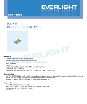
The 19-218/BHC-ZL1M2QY/3T is a surface-mount device (SMD) light-emitting diode (LED) designed for modern, compact electronic applications. This component represents a significant advancement over traditional lead-frame type LEDs, enabling substantial miniaturization of end products. Its core value proposition lies in enabling smaller printed circuit board (PCB) designs, higher component packing density, and reduced overall equipment size and weight. This makes it an ideal choice for applications where space and weight are critical constraints.
The LED is a mono-color type, emitting blue light, and is constructed using environmentally friendly materials. It is fully compliant with major international regulations, including the European Union's Restriction of Hazardous Substances (RoHS) directive, Registration, Evaluation, Authorization and Restriction of Chemicals (REACH) regulation, and halogen-free requirements (Br <900 ppm, Cl <900 ppm, Br+Cl < 1500 ppm). The product is supplied in a tape-and-reel format compatible with standard automated pick-and-place assembly equipment, streamlining high-volume manufacturing processes.
1.1 Core Advantages and Target Market
The primary advantages of this SMD LED stem from its miniature footprint and lightweight construction. By eliminating bulky leads, it allows for more efficient use of PCB real estate. This directly translates to smaller final product enclosures, reduced material costs, and lighter end-user devices. The high packing density achievable with SMD components is crucial for modern, feature-rich electronics.
The target applications for this LED are diverse, focusing on indicator and backlighting functions. Key markets include automotive interiors (e.g., dashboard and switch backlighting), telecommunications equipment (e.g., status indicators and keypad backlighting in phones and fax machines), and consumer electronics (e.g., flat backlighting for liquid crystal displays (LCDs), switches, and symbols). Its general-purpose nature also makes it suitable for a wide array of other indicator applications across industrial and consumer sectors.
2. Absolute Maximum Ratings and Technical Parameters
Understanding the absolute maximum ratings is essential for ensuring reliable operation and preventing premature device failure. These ratings define the stress limits beyond which permanent damage may occur.
- Reverse Voltage (VR): 5 V. Exceeding this voltage in the reverse direction can cause junction breakdown.
- Continuous Forward Current (IF): 25 mA. This is the maximum DC current that can be applied continuously.
- Peak Forward Current (IFP): 100 mA. This pulsed current rating (at a duty cycle of 1/10 and 1 kHz frequency) allows for brief periods of higher brightness but must not be used for continuous operation.
- Power Dissipation (Pd): 95 mW. This is the maximum amount of power the device can dissipate as heat, calculated as the product of forward voltage and forward current.
- Electrostatic Discharge (ESD) Human Body Model (HBM): 150 V. Proper ESD handling procedures must be followed during assembly and handling to avoid damage from static electricity.
- Operating Temperature (Topr): -40°C to +85°C. The device is guaranteed to function within this ambient temperature range.
- Storage Temperature (Tstg): -40°C to +90°C.
- Soldering Temperature: The device can withstand reflow soldering with a peak temperature of 260°C for up to 10 seconds, or hand soldering at 350°C for up to 3 seconds per terminal.
3. Electro-Optical Characteristics
The electro-optical characteristics are measured at a standard test condition of an ambient temperature (Ta) of 25°C and a forward current (IF) of 5 mA, unless otherwise specified. These parameters define the light output and electrical behavior of the LED.
- Luminous Intensity (Iv): Ranges from a minimum of 11.5 millicandelas (mcd) to a maximum of 28.5 mcd. The typical value is not specified in the summary table, but the binning system provides specific ranges.
- Viewing Angle (2θ1/2): 120 degrees. This is the full angle at which the luminous intensity is half of the intensity at 0 degrees (on-axis). A wide viewing angle like this is suitable for applications requiring broad illumination or visibility from multiple angles.
- Peak Wavelength (λp): 468 nm. This is the wavelength at which the spectral power distribution reaches its maximum.
- Dominant Wavelength (λd): Ranges from 465 nm to 475 nm. This is the single wavelength perceived by the human eye that matches the color of the LED's light. It is a key parameter for color definition.
- Spectral Radiation Bandwidth (Δλ): 25 nm (typical). This defines the width of the emitted spectrum at half of the peak intensity.
- Forward Voltage (VF): Ranges from 2.7 V to 3.2 V at IF = 5mA. This is the voltage drop across the LED when it is conducting current.
- Reverse Current (IR): Maximum of 50 μA when a reverse voltage (VR) of 5V is applied.
Note on Tolerances: The luminous intensity has a tolerance of ±11%, the dominant wavelength has a tolerance of ±1 nm, and the forward voltage has a tolerance of ±0.05 V. These tolerances are accounted for in the binning system.
4. Binning System Explanation
To ensure color and brightness consistency in production, LEDs are sorted into bins based on key parameters. This allows designers to select components that meet specific application requirements for uniformity.
4.1 Luminous Intensity Binning
LEDs are categorized into four bins (L1, L2, M1, M2) based on their measured luminous intensity at IF = 5mA.
- Bin L1: 11.5 mcd to 14.5 mcd
- Bin L2: 14.5 mcd to 18.0 mcd
- Bin M1: 18.0 mcd to 22.5 mcd
- Bin M2: 22.5 mcd to 28.5 mcd
4.2 Dominant Wavelength Binning
LEDs are grouped by their dominant wavelength to control the shade of blue.
- Group Z: This group contains bins for blue LEDs.
- Bin X: 465 nm to 470 nm (a slightly shorter, potentially greener-blue)
- Bin Y: 470 nm to 475 nm (a slightly longer, potentially purer or deeper blue)
4.3 Forward Voltage Binning
LEDs are also binned by forward voltage (VF) to aid in circuit design, particularly for current-limiting resistor calculation and power supply design.
- Group Q: This group contains the forward voltage bins.
- Bin 29: 2.7 V to 2.8 V
- Bin 30: 2.8 V to 2.9 V
- Bin 31: 2.9 V to 3.0 V
- Bin 32: 3.0 V to 3.1 V
- Bin 33: 3.1 V to 3.2 V
The full product part number (e.g., BHC-ZL1M2QY/3T) incorporates codes that specify which bins the device belongs to for luminous intensity, dominant wavelength, and forward voltage.
5. Performance Curve Analysis
The datasheet provides several characteristic curves that illustrate how the LED's performance changes under different operating conditions. These are critical for robust design.
5.1 Luminous Intensity vs. Forward Current
This curve shows that luminous intensity increases with forward current, but the relationship is not perfectly linear, especially at higher currents. Operating above the recommended continuous current will increase light output but also generate more heat, potentially reducing lifespan and shifting color.
5.2 Luminous Intensity vs. Ambient Temperature
As the ambient temperature increases, the luminous intensity of the LED decreases. This is a fundamental characteristic of semiconductor light sources. The curve shows the relative luminous intensity dropping as temperature rises from -40°C to +100°C. Designs for high-temperature environments must account for this derating.
5.3 Forward Current Derating Curve
To prevent overheating, the maximum allowable continuous forward current must be reduced as the ambient temperature increases. This curve provides the derating information, specifying the lower IF limits at higher Ta to stay within the power dissipation rating.
5.4 Forward Voltage vs. Forward Current
This is the current-voltage (I-V) characteristic of the LED diode. It shows the exponential relationship, where a small increase in voltage beyond the turn-on threshold causes a large increase in current. This highlights the critical need for a current-limiting device (like a resistor or constant-current driver) in series with the LED.
5.5 Spectral Distribution
The graph depicts the relative radiant power emitted across the visible light spectrum, centered around the peak wavelength of 468 nm with a typical bandwidth of 25 nm. This defines the purity and specific hue of the blue light.
5.6 Radiation Diagram
This polar plot visually represents the spatial distribution of light, confirming the 120-degree viewing angle. It shows how intensity diminishes at angles off the central axis.
6. Mechanical and Packaging Information
The physical dimensions of the SMD LED package are provided in detailed drawings. Key dimensions include the overall length, width, and height, as well as the placement and size of the solderable terminals. A recommended solder pad layout is also suggested to ensure a reliable solder joint and proper alignment during reflow. The pad design is for reference, and designers may modify it based on their specific PCB manufacturing capabilities and thermal management needs. Tolerances for package dimensions are typically ±0.1 mm unless otherwise noted.
The component features a clear (colorless) resin lens, allowing the blue light from the InGaN (Indium Gallium Nitride) semiconductor chip to be emitted without color filtering. Polarity is indicated by a marking on the package, which must be observed during placement to ensure correct electrical connection.
7. Soldering, Assembly, and Storage Guidelines
Adherence to these guidelines is paramount for assembly yield and long-term reliability.
7.1 Current Limiting Requirement
An external current-limiting resistor is mandatory. The LED's exponential I-V characteristic means that a small change in supply voltage can cause a large, potentially destructive change in forward current. The resistor sets the operating current reliably.
7.2 Storage and Moisture Sensitivity
The LEDs are packaged in a moisture-resistant bag with desiccant to prevent absorption of atmospheric moisture. The bag should not be opened until the components are ready for use in production. Before opening, storage conditions should be ≤30°C and ≤90% RH. After opening, the components have a "floor life" of one year if kept at ≤30°C and ≤60% RH. Unused parts should be resealed in a moisture-proof package. If the desiccant indicator changes color or the storage time is exceeded, a baking treatment at 60 ±5°C for 24 hours is required to remove moisture before reflow soldering.
7.3 Soldering Conditions
The device is compatible with infrared (IR) and vapor phase reflow soldering processes. A Pb-free reflow temperature profile is provided, specifying pre-heating, time above liquidus (217°C), peak temperature (max 260°C for 10 sec max), and cooling rates. Reflow soldering should not be performed more than two times on the same LED. During soldering, no mechanical stress should be applied to the component, and the PCB should not be warped after the process.
7.4 Hand Soldering and Rework
If hand soldering is necessary, the iron tip temperature must be below 350°C, and contact time per terminal should not exceed 3 seconds. A low-power iron (<25W) is recommended, with an interval of at least 2 seconds between soldering each terminal. Rework after the LED is soldered is strongly discouraged. If absolutely unavoidable, a specialized double-head soldering iron must be used to simultaneously heat both terminals, and the impact on LED characteristics must be verified beforehand.
8. Packaging and Ordering Information
The product is supplied in a standard 8mm tape on a 7-inch diameter reel. Each reel contains 3000 pieces. The carrier tape and reel dimensions are specified to ensure compatibility with automated assembly equipment. The packaging includes an aluminum moisture-proof bag, desiccant, and labels. The label on the reel provides critical information including the product number (P/N), customer part number (CPN), packing quantity (QTY), and the specific bin codes for luminous intensity (CAT), dominant wavelength/chromaticity (HUE), and forward voltage (REF), along with the manufacturing lot number (LOT No).
9. Application Design Considerations
9.1 Circuit Design
The fundamental design step is selecting an appropriate current-limiting resistor. The value is calculated using Ohm's Law: R = (Vsupply - VF) / IF. Use the maximum VF from the datasheet (or the specific bin) to ensure the current does not exceed the desired IF under worst-case conditions. The resistor's power rating must also be sufficient: PR = (IF)² * R. For designs requiring consistent brightness across a temperature range or multiple LEDs, consider using a constant-current driver instead of a simple resistor.
9.2 Thermal Management
While SMD LEDs are efficient, they still generate heat. Operating at or near the maximum current rating will increase junction temperature. High temperatures reduce light output (lumen depreciation) and can accelerate long-term degradation. Ensure the PCB layout provides adequate thermal relief, especially if the LED is driven at high currents or used in a high ambient temperature environment. Follow the forward current derating curve provided in the datasheet.
9.3 Optical Integration
The 120-degree viewing angle provides broad emission. For applications requiring a more focused beam, secondary optics such as lenses or light guides may be necessary. The clear resin package is suitable for use with external optical elements. When designing light guides or diffusers, account for the LED's spatial radiation pattern and spectral output.
10. Technical Comparison and Differentiation
Compared to traditional through-hole LEDs with wire leads, this SMD LED offers decisive advantages for modern manufacturing: drastically reduced board space, suitability for fully automated assembly, and lower profile enabling thinner products. Within the SMD LED category, key differentiators for this specific part include its combination of a relatively high luminous intensity binning range (up to 28.5 mcd at 5mA), a very wide 120-degree viewing angle, and compliance with stringent halogen-free and RoHS standards. The detailed binning system for intensity, wavelength, and voltage provides designers with the granularity needed for applications demanding high consistency, such as multi-LED backlight arrays or status indicator clusters where color and brightness matching are visually important.
11. Frequently Asked Questions (FAQ)
Q: Why is a current-limiting resistor absolutely necessary?
A: LEDs are diodes with a non-linear, exponential current-voltage relationship. Without a resistor to limit current, even a small excess voltage would cause the current to rise uncontrollably, almost instantly destroying the LED due to overheating.
Q: Can I drive this LED with a 3.3V supply without a resistor?
A: No. The forward voltage ranges from 2.7V to 3.2V. A 3.3V supply exceeds the minimum VF, and without a resistor to drop the extra 0.1V to 0.6V, the current would be unregulated and likely exceed the maximum rating, damaging the LED.
Q: What does the "Pb-free" designation mean for soldering?
A> It means the device's terminations are free of lead. This requires the use of lead-free (Pb-free) solder alloys during assembly, which typically have higher melting points than traditional tin-lead solder. The provided reflow profile is specifically designed for these higher-temperature Pb-free processes.
Q: How do I interpret the part number bin codes (e.g., ZL1M2QY)?
A> The codes correspond to the binning groups. For example, 'L1' or 'M2' indicates the luminous intensity bin, 'Y' indicates the dominant wavelength bin (470-475nm), and 'QY' likely references the forward voltage bin group. The exact mapping should be confirmed with the manufacturer's detailed bin code documentation.
12. Design and Use Case Examples
Case 1: Automotive Dashboard Switch Backlighting: A cluster of 5-10 of these LEDs is used to backlight various buttons and knobs. The designer selects LEDs from the same luminous intensity bin (e.g., M1) and dominant wavelength bin (e.g., Y) to ensure uniform color and brightness across all switches. The wide 120° viewing angle ensures the backlight is visible from the driver's perspective. The LEDs are driven at a conservative 10mA via a constant-current regulator integrated into the dashboard control module to maintain stable brightness despite fluctuations in the vehicle's 12V electrical system.
Case 2: Industrial Status Indicator Panel: A single LED is used as a "power on" indicator on a piece of factory equipment. A simple circuit is designed with a 5V rail, a current-limiting resistor calculated for 15mA operation (using max VF of 3.2V: R = (5-3.2)/0.015 = 120Ω), and the LED. The clear blue light is highly visible in a well-lit industrial environment. The SMD package allows it to be placed directly on the main control PCB, saving space and assembly cost compared to a panel-mounted through-hole LED.
13. Operating Principle
This LED is a semiconductor photonic device. Its core is a chip made of InGaN (Indium Gallium Nitride) materials. When a forward voltage exceeding the diode's turn-on threshold is applied, electrons and holes are injected into the active region of the semiconductor. These charge carriers recombine, and the energy released from this recombination is emitted in the form of photons (light). The specific composition of the InGaN alloy determines the bandgap energy of the semiconductor, which directly dictates the wavelength (color) of the emitted light—in this case, blue. The clear epoxy resin encapsulant protects the delicate semiconductor chip, acts as a lens to shape the light output, and provides mechanical stability.
14. Technology Trends
The development of SMD LEDs like the 19-218 series is part of the broader trend in electronics towards miniaturization, increased functionality per unit area, and automated, high-volume manufacturing. Advancements in semiconductor materials, particularly in the efficiency and color range of InGaN-based blue and white LEDs, have been a primary driver. Future trends in this class of components may include further increases in luminous efficacy (more light output per electrical watt), improved color consistency and rendering, integration of onboard control circuitry (becoming "smart" LEDs), and packages designed for even higher power densities and better thermal management. The push for sustainability continues to drive the elimination of hazardous substances and improvements in energy efficiency across the lifecycle.
LED Specification Terminology
Complete explanation of LED technical terms
Photoelectric Performance
| Term | Unit/Representation | Simple Explanation | Why Important |
|---|---|---|---|
| Luminous Efficacy | lm/W (lumens per watt) | Light output per watt of electricity, higher means more energy efficient. | Directly determines energy efficiency grade and electricity cost. |
| Luminous Flux | lm (lumens) | Total light emitted by source, commonly called "brightness". | Determines if the light is bright enough. |
| Viewing Angle | ° (degrees), e.g., 120° | Angle where light intensity drops to half, determines beam width. | Affects illumination range and uniformity. |
| CCT (Color Temperature) | K (Kelvin), e.g., 2700K/6500K | Warmth/coolness of light, lower values yellowish/warm, higher whitish/cool. | Determines lighting atmosphere and suitable scenarios. |
| CRI / Ra | Unitless, 0–100 | Ability to render object colors accurately, Ra≥80 is good. | Affects color authenticity, used in high-demand places like malls, museums. |
| SDCM | MacAdam ellipse steps, e.g., "5-step" | Color consistency metric, smaller steps mean more consistent color. | Ensures uniform color across same batch of LEDs. |
| Dominant Wavelength | nm (nanometers), e.g., 620nm (red) | Wavelength corresponding to color of colored LEDs. | Determines hue of red, yellow, green monochrome LEDs. |
| Spectral Distribution | Wavelength vs intensity curve | Shows intensity distribution across wavelengths. | Affects color rendering and quality. |
Electrical Parameters
| Term | Symbol | Simple Explanation | Design Considerations |
|---|---|---|---|
| Forward Voltage | Vf | Minimum voltage to turn on LED, like "starting threshold". | Driver voltage must be ≥Vf, voltages add up for series LEDs. |
| Forward Current | If | Current value for normal LED operation. | Usually constant current drive, current determines brightness & lifespan. |
| Max Pulse Current | Ifp | Peak current tolerable for short periods, used for dimming or flashing. | Pulse width & duty cycle must be strictly controlled to avoid damage. |
| Reverse Voltage | Vr | Max reverse voltage LED can withstand, beyond may cause breakdown. | Circuit must prevent reverse connection or voltage spikes. |
| Thermal Resistance | Rth (°C/W) | Resistance to heat transfer from chip to solder, lower is better. | High thermal resistance requires stronger heat dissipation. |
| ESD Immunity | V (HBM), e.g., 1000V | Ability to withstand electrostatic discharge, higher means less vulnerable. | Anti-static measures needed in production, especially for sensitive LEDs. |
Thermal Management & Reliability
| Term | Key Metric | Simple Explanation | Impact |
|---|---|---|---|
| Junction Temperature | Tj (°C) | Actual operating temperature inside LED chip. | Every 10°C reduction may double lifespan; too high causes light decay, color shift. |
| Lumen Depreciation | L70 / L80 (hours) | Time for brightness to drop to 70% or 80% of initial. | Directly defines LED "service life". |
| Lumen Maintenance | % (e.g., 70%) | Percentage of brightness retained after time. | Indicates brightness retention over long-term use. |
| Color Shift | Δu′v′ or MacAdam ellipse | Degree of color change during use. | Affects color consistency in lighting scenes. |
| Thermal Aging | Material degradation | Deterioration due to long-term high temperature. | May cause brightness drop, color change, or open-circuit failure. |
Packaging & Materials
| Term | Common Types | Simple Explanation | Features & Applications |
|---|---|---|---|
| Package Type | EMC, PPA, Ceramic | Housing material protecting chip, providing optical/thermal interface. | EMC: good heat resistance, low cost; Ceramic: better heat dissipation, longer life. |
| Chip Structure | Front, Flip Chip | Chip electrode arrangement. | Flip chip: better heat dissipation, higher efficacy, for high-power. |
| Phosphor Coating | YAG, Silicate, Nitride | Covers blue chip, converts some to yellow/red, mixes to white. | Different phosphors affect efficacy, CCT, and CRI. |
| Lens/Optics | Flat, Microlens, TIR | Optical structure on surface controlling light distribution. | Determines viewing angle and light distribution curve. |
Quality Control & Binning
| Term | Binning Content | Simple Explanation | Purpose |
|---|---|---|---|
| Luminous Flux Bin | Code e.g., 2G, 2H | Grouped by brightness, each group has min/max lumen values. | Ensures uniform brightness in same batch. |
| Voltage Bin | Code e.g., 6W, 6X | Grouped by forward voltage range. | Facilitates driver matching, improves system efficiency. |
| Color Bin | 5-step MacAdam ellipse | Grouped by color coordinates, ensuring tight range. | Guarantees color consistency, avoids uneven color within fixture. |
| CCT Bin | 2700K, 3000K etc. | Grouped by CCT, each has corresponding coordinate range. | Meets different scene CCT requirements. |
Testing & Certification
| Term | Standard/Test | Simple Explanation | Significance |
|---|---|---|---|
| LM-80 | Lumen maintenance test | Long-term lighting at constant temperature, recording brightness decay. | Used to estimate LED life (with TM-21). |
| TM-21 | Life estimation standard | Estimates life under actual conditions based on LM-80 data. | Provides scientific life prediction. |
| IESNA | Illuminating Engineering Society | Covers optical, electrical, thermal test methods. | Industry-recognized test basis. |
| RoHS / REACH | Environmental certification | Ensures no harmful substances (lead, mercury). | Market access requirement internationally. |
| ENERGY STAR / DLC | Energy efficiency certification | Energy efficiency and performance certification for lighting. | Used in government procurement, subsidy programs, enhances competitiveness. |