Table of Contents
- 1. Product Overview
- 2. Technical Specifications Deep Dive
- 2.1 Absolute Maximum Ratings
- 2.2 Electro-Optical Characteristics
- 3. Binning System Explanation
- 3.1 Luminous Intensity Bins
- 3.2 Dominant Wavelength Bins
- 3.3 Forward Voltage Bins
- 4. Performance Curve Analysis
- 4.1 Radiation Pattern
- 4.2 Relative Luminous Intensity vs. Forward Current
- 4.3 Relative Luminous Intensity vs. Ambient Temperature
- 4.4 Forward Current Derating Curve
- 4.5 Forward Voltage vs. Forward Current
- 4.6 Spectrum Distribution
- 5. Mechanical & Packaging Information
- 5.1 Package Dimensions
- 5.2 Reel, Tape, and Moisture-Sensitive Packaging
- 6. Soldering & Assembly Guidelines
- 6.1 Storage and Handling Precautions
- 6.2 Reflow Soldering Profile
- 6.3 Hand Soldering & Rework
- 6.4 Circuit Design Consideration
- 7. Application Suggestions
- 7.1 Typical Application Scenarios
- 7.2 Design Considerations
- 8. Technical Comparison & Differentiation
- 9. Frequently Asked Questions (Based on Technical Parameters)
- 10. Design and Usage Case Study
- 11. Operating Principle Introduction
- 12. Technology Trends
- LED Specification Terminology
- Photoelectric Performance
- Electrical Parameters
- Thermal Management & Reliability
- Packaging & Materials
- Quality Control & Binning
- Testing & Certification
1. Product Overview
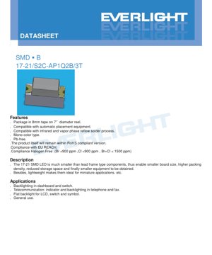
The 17-21/S2C-AP1Q2B/3T is a surface-mount device (SMD) LED designed for high-density electronic assemblies. Its primary function is to provide a brilliant orange indication or backlighting. The core advantage of this component lies in its miniature footprint, measuring approximately 2.0mm x 1.25mm, which enables significant space savings on printed circuit boards (PCBs) compared to traditional leaded LEDs. This reduction in size directly contributes to smaller end-product designs, reduced storage requirements for components, and higher packing density on assembly reels and PCBs. The device is constructed using an AIGaInP (Aluminum Gallium Indium Phosphide) semiconductor chip, which is encapsulated in a water-clear resin lens. This material combination is responsible for producing its characteristic brilliant orange emitted color. The product is fully compliant with modern environmental regulations, being Pb-free, RoHS compliant, EU REACH compliant, and halogen-free (with Bromine <900ppm, Chlorine <900ppm, Br+Cl < 1500ppm). It is supplied on 8mm tape mounted on 7-inch diameter reels, making it fully compatible with high-speed automated pick-and-place assembly equipment.
2. Technical Specifications Deep Dive
2.1 Absolute Maximum Ratings
The device is designed to operate reliably within specified electrical and thermal limits. Exceeding these Absolute Maximum Ratings may cause permanent damage. The maximum reverse voltage (VR) is 5V. The continuous forward current (IF) should not exceed 25mA. For pulsed operation, a peak forward current (IFP) of 60mA is permissible under a duty cycle of 1/10 at 1kHz. The total power dissipation (Pd) for the package is limited to 60mW. The device can withstand an electrostatic discharge (ESD) of 2000V per the Human Body Model (HBM). The operating temperature range (Topr) is from -40°C to +85°C, while the storage temperature range (Tstg) is slightly wider at -40°C to +90°C. For soldering, it can endure reflow profiles with a peak temperature of 260°C for up to 10 seconds, or hand soldering at 350°C for a maximum of 3 seconds per terminal.
2.2 Electro-Optical Characteristics
The key performance parameters are measured at a standard test condition of an ambient temperature (Ta) of 25°C and a forward current (IF) of 20mA. The luminous intensity (Iv) has a typical range from 45.00 mcd to 112.00 mcd, categorized into specific bins. The viewing angle (2θ1/2), defined as the full angle at half intensity, is typically 140 degrees, providing a wide emission pattern suitable for many indicator applications. The spectral characteristics are defined by a peak wavelength (λp) of 611 nm and a dominant wavelength (λd) range from 600.50 nm to 612.50 nm. The spectral bandwidth (Δλ) is approximately 17 nm. The forward voltage (VF) required to drive the LED at 20mA ranges from 1.75V to 2.35V, also organized into bins. The reverse current (IR) is guaranteed to be less than 10 μA when a reverse voltage of 5V is applied, though the device is not intended for reverse operation.
3. Binning System Explanation
To ensure color and brightness consistency in production, the LEDs are sorted into bins based on three key parameters: Luminous Intensity, Dominant Wavelength, and Forward Voltage.
3.1 Luminous Intensity Bins
The luminous output is categorized into four bins (P1, P2, Q1, Q2) when driven at IF=20mA. The P1 bin covers the range from 45.00 mcd to 57.00 mcd. P2 covers 57.00 mcd to 72.00 mcd. Q1 covers 72.00 mcd to 90.00 mcd. The highest output bin, Q2, covers 90.00 mcd to 112.00 mcd. A tolerance of ±11% applies within each bin.
3.2 Dominant Wavelength Bins
The dominant wavelength, which defines the perceived color, is sorted into four bins (D8, D9, D10, D11). D8 ranges from 600.50 nm to 603.50 nm. D9 ranges from 603.50 nm to 606.50 nm. D10 ranges from 606.50 nm to 609.50 nm. D11 ranges from 609.50 nm to 612.50 nm. A tolerance of ±1nm is specified.
3.3 Forward Voltage Bins
The forward voltage drop is sorted into three bins (0, 1, 2) to aid in circuit design, particularly for current-limiting resistor calculation. Bin 0 covers 1.75V to 1.95V. Bin 1 covers 1.95V to 2.15V. Bin 2 covers 2.15V to 2.35V. A tolerance of ±0.1V is noted.
4. Performance Curve Analysis
The datasheet provides several characteristic curves that are essential for understanding the LED's behavior under different conditions.
4.1 Radiation Pattern
The radiation diagram shows the spatial distribution of light intensity. The pattern is typically Lambertian or near-Lambertian, with the relative intensity plotted against the viewing angle. The 140-degree viewing angle confirms a wide, diffuse emission suitable for area illumination or indicators requiring wide visibility.
4.2 Relative Luminous Intensity vs. Forward Current
This curve illustrates the non-linear relationship between drive current and light output. The luminous intensity increases with current but will eventually saturate. Operating significantly above the recommended 20mA may lead to reduced efficiency and accelerated aging.
4.3 Relative Luminous Intensity vs. Ambient Temperature
This graph is critical for thermal management. The light output decreases as the ambient temperature rises. For example, at the maximum operating temperature of +85°C, the output may be significantly lower than at 25°C. This must be accounted for in designs where consistent brightness is required across a temperature range.
4.4 Forward Current Derating Curve
This curve defines the maximum allowable forward current as a function of ambient temperature. As temperature increases, the maximum safe current decreases to prevent exceeding the 60mW power dissipation limit and to manage junction temperature, ensuring long-term reliability.
4.5 Forward Voltage vs. Forward Current
This IV (Current-Voltage) characteristic shows the exponential relationship typical of a diode. Knowing this curve helps in designing an appropriate current-limiting circuit.
4.6 Spectrum Distribution
The spectral power distribution plot shows the intensity of emitted light across wavelengths, centered around the 611nm peak. The narrow bandwidth (~17nm) indicates a relatively pure orange color.
5. Mechanical & Packaging Information
5.1 Package Dimensions
The LED has a compact rectangular package. Key dimensions include the overall length, width, and height. The cathode is identified by a specific mark on the package body, which is crucial for correct orientation during assembly. All unspecified tolerances are typically ±0.1mm.
5.2 Reel, Tape, and Moisture-Sensitive Packaging
The components are supplied in moisture-resistant packaging. They are housed in a carrier tape with specific pocket dimensions, wound onto a 7-inch diameter reel. Each reel contains 3000 pieces. The packaging includes a desiccant and is sealed within an aluminum moisture-proof bag. Labels on the bag provide critical information: Customer's Product Number (CPN), Product Number (P/N), Packing Quantity (QTY), Luminous Intensity Rank (CAT), Chromaticity/Dominant Wavelength Rank (HUE), Forward Voltage Rank (REF), and Lot Number (LOT No).
6. Soldering & Assembly Guidelines
6.1 Storage and Handling Precautions
The LEDs are moisture-sensitive devices (MSD). The unopened moisture-proof bag must not be opened until the components are ready for use. After opening, unused LEDs should be stored at conditions of 30°C or less and 60% relative humidity or less. The "floor life" after bag opening is 168 hours (7 days). If components exceed this time or if the desiccant indicator has changed color, a baking treatment at 60 ±5°C for 24 hours is required before use to remove absorbed moisture and prevent "popcorning" during reflow soldering.
6.2 Reflow Soldering Profile
A lead-free reflow soldering profile is specified. Key parameters include: a pre-heating stage between 150-200°C for 60-120 seconds; a time above liquidus (217°C) of 60-150 seconds; a peak temperature not exceeding 260°C, held for a maximum of 10 seconds; maximum heating and cooling rates. Reflow soldering should not be performed more than two times on the same component.
6.3 Hand Soldering & Rework
If hand soldering is necessary, extreme care must be taken. The soldering iron tip temperature should be less than 350°C, applied to each terminal for no more than 3 seconds. The soldering iron power should be 25W or less. A minimum interval of 2 seconds should be left between soldering each terminal. Rework is strongly discouraged. If unavoidable, a dual-head soldering iron should be used to simultaneously heat both terminals and avoid mechanical stress on the solder joints. The potential for damage to the LED during rework is high.
6.4 Circuit Design Consideration
An external current-limiting resistor is mandatory. The LED's forward voltage has a negative temperature coefficient, meaning it decreases as temperature rises. Without a series resistor, a small increase in supply voltage or a decrease in VF could cause a large, potentially destructive, increase in forward current. The resistor value must be calculated based on the supply voltage, the forward voltage bin of the LED, and the desired operating current (typically 20mA or less).
7. Application Suggestions
7.1 Typical Application Scenarios
The brilliant orange color and small size make this LED suitable for a variety of applications: Backlighting for instrument panel dashboards, switches, and symbols; Status indicators in telecommunications equipment such as telephones and fax machines; General-purpose indicator lights in consumer electronics, industrial controls, and automotive interiors; Flat backlighting for small LCD panels.
7.2 Design Considerations
When integrating this LED, designers must consider several factors: Current Drive: Always use a constant current source or a voltage source with a series resistor. Thermal Management: Ensure adequate PCB copper area or thermal vias if operating at high ambient temperatures or near maximum current to manage junction temperature. Optical Design: The wide viewing angle may require light guides or diffusers to shape the light for specific applications. ESD Protection: Implement standard ESD precautions during handling and assembly, as the 2000V HBM rating, while robust, can be exceeded in uncontrolled environments.
8. Technical Comparison & Differentiation
Compared to older through-hole LED technologies, this SMD LED offers substantial advantages: a reduction in board space by over 70%, compatibility with fully automated assembly reducing labor costs, and improved reliability due to the absence of bent leads. Within the SMD LED market, its key differentiators are the use of AIGaInP technology for high-efficiency orange light (superior to filtered or dyed LEDs), specific compliance with halogen-free requirements, and a detailed binning structure that allows for precise color and brightness matching in production runs. The combination of a relatively high luminous intensity for its size and a low forward voltage contributes to good overall power efficiency.
9. Frequently Asked Questions (Based on Technical Parameters)
Q: What resistor value should I use with a 5V supply?
A: The value depends on the LED's forward voltage (VF) bin. Using the worst-case (lowest VF) of 1.75V and a target current of 20mA: R = (Vsupply - Vf) / If = (5V - 1.75V) / 0.02A = 162.5 Ohms. A standard 160 or 180 Ohm resistor would be suitable. Always calculate for the specific VF bin you are using and verify power dissipation in the resistor.
Q: Can I drive this LED with a PWM signal for dimming?
A: Yes, pulse-width modulation (PWM) is an effective method for dimming LEDs. Ensure the peak current in each pulse does not exceed the 60mA rating, and the average current over time does not exceed the 25mA continuous rating. A frequency of 100Hz to 1kHz is typical.
Q: Why is the storage time after bag opening limited to 7 days?
A: The plastic packaging material can absorb moisture from the air. During the high-temperature reflow soldering process, this trapped moisture can rapidly expand into steam, causing internal delamination or cracking ("popcorning"), which destroys the component. The 7-day limit is based on the moisture sensitivity level (MSL) of the package.
Q: How does temperature affect the light output?
A: Light output has a negative temperature coefficient. As the junction temperature increases, the luminous efficiency decreases, resulting in lower light output for the same drive current. The performance curves in section 4 quantify this relationship, which is critical for applications operating in hot environments.
10. Design and Usage Case Study
Scenario: Designing a multi-indicator status panel for an industrial controller. The panel requires 20 identical brilliant orange LEDs to show various system states. To ensure uniform appearance, specifying LEDs from the same luminous intensity bin (e.g., Q1) and the same dominant wavelength bin (e.g., D10) is essential. The PCB layout must include correctly sized pads per the package drawing and a current-limiting resistor for each LED, calculated based on the system's 3.3V logic supply and the chosen VF bin. To simplify assembly, the design should use the tape-and-reel format directly with automated placement equipment. The manufacturing process must adhere to the reflow profile and manage the 7-day floor life for the opened reel to prevent moisture-related yield loss. Thermal analysis should confirm that placing 20 LEDs in close proximity does not cause localized heating that would derate the maximum allowable current.
11. Operating Principle Introduction
Light emission in this LED is based on electroluminescence in a semiconductor p-n junction made of AIGaInP (Aluminum Gallium Indium Phosphide). When a forward voltage exceeding the junction's built-in potential is applied, electrons from the n-type region and holes from the p-type region are injected into the active region. Here, they recombine, releasing energy in the form of photons. The specific bandgap energy of the AIGaInP alloy determines the wavelength (color) of the emitted light, which in this case is in the orange spectrum (~611 nm). The water-clear epoxy resin encapsulant protects the semiconductor chip, provides mechanical stability, and acts as a lens to shape the light output pattern.
12. Technology Trends
The general trend in SMD indicator LEDs continues toward higher efficiency (more lumens or millicandelas per watt), smaller package sizes for increased density, and improved color consistency through tighter binning. There is also a strong drive for higher reliability and longer lifetime under a wider range of environmental conditions, including higher temperature operation for automotive and industrial applications. Integration of features, such as built-in current-limiting resistors or protection diodes within the same package, is another ongoing development to simplify circuit design and save board space further. Environmental compliance, including halogen-free materials and full RoHS adherence, has become a standard requirement rather than a differentiator.
LED Specification Terminology
Complete explanation of LED technical terms
Photoelectric Performance
| Term | Unit/Representation | Simple Explanation | Why Important |
|---|---|---|---|
| Luminous Efficacy | lm/W (lumens per watt) | Light output per watt of electricity, higher means more energy efficient. | Directly determines energy efficiency grade and electricity cost. |
| Luminous Flux | lm (lumens) | Total light emitted by source, commonly called "brightness". | Determines if the light is bright enough. |
| Viewing Angle | ° (degrees), e.g., 120° | Angle where light intensity drops to half, determines beam width. | Affects illumination range and uniformity. |
| CCT (Color Temperature) | K (Kelvin), e.g., 2700K/6500K | Warmth/coolness of light, lower values yellowish/warm, higher whitish/cool. | Determines lighting atmosphere and suitable scenarios. |
| CRI / Ra | Unitless, 0–100 | Ability to render object colors accurately, Ra≥80 is good. | Affects color authenticity, used in high-demand places like malls, museums. |
| SDCM | MacAdam ellipse steps, e.g., "5-step" | Color consistency metric, smaller steps mean more consistent color. | Ensures uniform color across same batch of LEDs. |
| Dominant Wavelength | nm (nanometers), e.g., 620nm (red) | Wavelength corresponding to color of colored LEDs. | Determines hue of red, yellow, green monochrome LEDs. |
| Spectral Distribution | Wavelength vs intensity curve | Shows intensity distribution across wavelengths. | Affects color rendering and quality. |
Electrical Parameters
| Term | Symbol | Simple Explanation | Design Considerations |
|---|---|---|---|
| Forward Voltage | Vf | Minimum voltage to turn on LED, like "starting threshold". | Driver voltage must be ≥Vf, voltages add up for series LEDs. |
| Forward Current | If | Current value for normal LED operation. | Usually constant current drive, current determines brightness & lifespan. |
| Max Pulse Current | Ifp | Peak current tolerable for short periods, used for dimming or flashing. | Pulse width & duty cycle must be strictly controlled to avoid damage. |
| Reverse Voltage | Vr | Max reverse voltage LED can withstand, beyond may cause breakdown. | Circuit must prevent reverse connection or voltage spikes. |
| Thermal Resistance | Rth (°C/W) | Resistance to heat transfer from chip to solder, lower is better. | High thermal resistance requires stronger heat dissipation. |
| ESD Immunity | V (HBM), e.g., 1000V | Ability to withstand electrostatic discharge, higher means less vulnerable. | Anti-static measures needed in production, especially for sensitive LEDs. |
Thermal Management & Reliability
| Term | Key Metric | Simple Explanation | Impact |
|---|---|---|---|
| Junction Temperature | Tj (°C) | Actual operating temperature inside LED chip. | Every 10°C reduction may double lifespan; too high causes light decay, color shift. |
| Lumen Depreciation | L70 / L80 (hours) | Time for brightness to drop to 70% or 80% of initial. | Directly defines LED "service life". |
| Lumen Maintenance | % (e.g., 70%) | Percentage of brightness retained after time. | Indicates brightness retention over long-term use. |
| Color Shift | Δu′v′ or MacAdam ellipse | Degree of color change during use. | Affects color consistency in lighting scenes. |
| Thermal Aging | Material degradation | Deterioration due to long-term high temperature. | May cause brightness drop, color change, or open-circuit failure. |
Packaging & Materials
| Term | Common Types | Simple Explanation | Features & Applications |
|---|---|---|---|
| Package Type | EMC, PPA, Ceramic | Housing material protecting chip, providing optical/thermal interface. | EMC: good heat resistance, low cost; Ceramic: better heat dissipation, longer life. |
| Chip Structure | Front, Flip Chip | Chip electrode arrangement. | Flip chip: better heat dissipation, higher efficacy, for high-power. |
| Phosphor Coating | YAG, Silicate, Nitride | Covers blue chip, converts some to yellow/red, mixes to white. | Different phosphors affect efficacy, CCT, and CRI. |
| Lens/Optics | Flat, Microlens, TIR | Optical structure on surface controlling light distribution. | Determines viewing angle and light distribution curve. |
Quality Control & Binning
| Term | Binning Content | Simple Explanation | Purpose |
|---|---|---|---|
| Luminous Flux Bin | Code e.g., 2G, 2H | Grouped by brightness, each group has min/max lumen values. | Ensures uniform brightness in same batch. |
| Voltage Bin | Code e.g., 6W, 6X | Grouped by forward voltage range. | Facilitates driver matching, improves system efficiency. |
| Color Bin | 5-step MacAdam ellipse | Grouped by color coordinates, ensuring tight range. | Guarantees color consistency, avoids uneven color within fixture. |
| CCT Bin | 2700K, 3000K etc. | Grouped by CCT, each has corresponding coordinate range. | Meets different scene CCT requirements. |
Testing & Certification
| Term | Standard/Test | Simple Explanation | Significance |
|---|---|---|---|
| LM-80 | Lumen maintenance test | Long-term lighting at constant temperature, recording brightness decay. | Used to estimate LED life (with TM-21). |
| TM-21 | Life estimation standard | Estimates life under actual conditions based on LM-80 data. | Provides scientific life prediction. |
| IESNA | Illuminating Engineering Society | Covers optical, electrical, thermal test methods. | Industry-recognized test basis. |
| RoHS / REACH | Environmental certification | Ensures no harmful substances (lead, mercury). | Market access requirement internationally. |
| ENERGY STAR / DLC | Energy efficiency certification | Energy efficiency and performance certification for lighting. | Used in government procurement, subsidy programs, enhances competitiveness. |