Table of Contents
- 1. Product Overview
- 1.1 Core Advantages and Target Market
- 2. Technical Parameter Deep Dive
- 2.1 Absolute Maximum Ratings
- 2.2 Electro-Optical Characteristics
- 3. Binning System Explanation
- 3.1 Luminous Intensity Binning
- 3.2 Dominant Wavelength Binning
- 3.3 Forward Voltage Binning
- 4. Performance Curve Analysis
- 5. Mechanical and Package Information
- 5.1 Package Dimensions
- 5.2 Polarity Identification
- 6. Soldering and Assembly Guidelines
- 6.1 Reflow Soldering Profile
- 6.2 Hand Soldering
- 6.3 Storage and Moisture Sensitivity
- 7. Packaging and Ordering Information
- 7.1 Packaging Specification
- 7.2 Label Explanation
- 8. Application Suggestions
- 8.1 Typical Application Scenarios
- 8.2 Design Considerations
- 9. Technical Comparison and Differentiation
- 10. Frequently Asked Questions (Based on Technical Parameters)
- 10.1 Why is a series resistor mandatory?
- 10.2 Can I drive this LED with a 3.3V or 5V supply?
- 10.3 What does the "binning" information mean for my design?
- 11. Practical Design and Usage Case
- 12. Operating Principle Introduction
- 13. Technology Trends
1. Product Overview
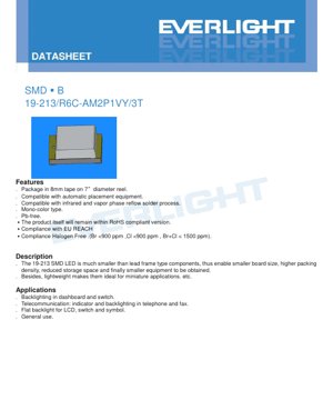
The 19-213 is a surface-mount device (SMD) LED designed for general-purpose indicator and backlighting applications. It utilizes an AlGaInP (Aluminum Gallium Indium Phosphide) chip to produce a brilliant red light output. This component is characterized by its compact size, which facilitates higher packing density on printed circuit boards (PCBs) and enables the design of smaller end-user equipment. The device is supplied on 8mm tape reels, making it fully compatible with automated pick-and-place assembly processes.
1.1 Core Advantages and Target Market
The primary advantages of this LED include its miniature footprint, lightweight construction, and compliance with modern manufacturing and environmental standards. It is Pb-free, RoHS compliant, REACH compliant, and classified as halogen-free. These features make it suitable for a wide range of consumer electronics, telecommunications equipment (e.g., telephones, fax machines), automotive dashboard and switch backlighting, and general backlighting for LCDs and symbols.
2. Technical Parameter Deep Dive
This section provides a detailed, objective interpretation of the key electrical, optical, and thermal parameters specified in the datasheet.
2.1 Absolute Maximum Ratings
These ratings define the stress limits beyond which permanent damage to the device may occur. Operation outside these limits is not advised.
- Reverse Voltage (VR): 5V. Exceeding this voltage in reverse bias can cause junction breakdown.
- Forward Current (IF): 25mA DC. The continuous DC current should not surpass this value.
- Peak Forward Current (IFP): 60mA. This is permissible only under pulsed conditions (duty cycle 1/10, 1kHz) to handle transient surges.
- Power Dissipation (Pd): 60mW. This is the maximum power the package can dissipate at an ambient temperature (Ta) of 25°C.
- Electrostatic Discharge (ESD): 2000V (Human Body Model). Proper ESD handling procedures are essential during assembly.
- Operating & Storage Temperature: -40°C to +85°C (operating), -40°C to +90°C (storage).
- Soldering Temperature: Reflow profile peak at 260°C for max 10 seconds; hand soldering at 350°C for max 3 seconds per terminal.
2.2 Electro-Optical Characteristics
These parameters are measured at a standard test condition of IF = 5mA and Ta = 25°C. They define the typical performance of the device.
- Luminous Intensity (Iv): Ranges from 22.5 mcd (min) to 57.0 mcd (max), with a typical tolerance of ±11%. The actual value is determined by the bin code (M2, N1, N2, P1).
- Viewing Angle (2θ1/2): A wide 120-degree typical angle, providing a broad emission pattern suitable for area illumination.
- Peak Wavelength (λp): Typically 632 nm, placing the emission in the red region of the visible spectrum.
- Dominant Wavelength (λd): Specified between 617.5 nm and 633.5 nm, with a tolerance of ±1 nm. This is the primary color coordinate, binned as E4 to E7.
- Spectral Bandwidth (Δλ): Typically 20 nm, indicating the spectral purity of the red light.
- Forward Voltage (VF): Ranges from 1.70V to 2.20V at 5mA, with a tolerance of ±0.05V. It is binned from code 19 to 23. A current-limiting resistor is mandatory in series to prevent thermal runaway from minor voltage fluctuations.
- Reverse Current (IR): Maximum 10 µA at VR=5V. The device is not designed for operation in reverse bias.
3. Binning System Explanation
The product is sorted into bins based on key performance parameters to ensure consistency within a production lot. Designers can specify bins to meet tight application requirements.
3.1 Luminous Intensity Binning
Bins: M2 (22.5-28.5 mcd), N1 (28.5-36.0 mcd), N2 (36.0-45.0 mcd), P1 (45.0-57.0 mcd). Selecting a higher bin (e.g., P1) guarantees higher minimum brightness.
3.2 Dominant Wavelength Binning
Bins: E4 (617.5-621.5 nm), E5 (621.5-625.5 nm), E6 (625.5-629.5 nm), E7 (629.5-633.5 nm). This allows for color consistency in applications where multiple LEDs are used side-by-side.
3.3 Forward Voltage Binning
Bins: 19 (1.70-1.80V), 20 (1.80-1.90V), 21 (1.90-2.00V), 22 (2.00-2.10V), 23 (2.10-2.20V). Matching VF bins can help achieve uniform current sharing in parallel configurations.
4. Performance Curve Analysis
While specific graphs are not detailed in the provided text, typical curves for such an LED would include:
- I-V (Current-Voltage) Curve: Shows the exponential relationship between forward voltage and current. The knee voltage is around 1.7-2.2V.
- Luminous Intensity vs. Forward Current: Intensity increases with current but may saturate at higher currents due to thermal effects.
- Luminous Intensity vs. Ambient Temperature: Intensity typically decreases as ambient temperature rises, a critical factor for thermal management.
- Spectral Distribution: A plot showing the relative radiant power versus wavelength, centered around 632 nm with a ~20 nm bandwidth.
5. Mechanical and Package Information
5.1 Package Dimensions
The LED comes in a standard SMD package. The dimensional drawing specifies the length, width, height, pad sizes, and their positions with a typical tolerance of ±0.1mm. Correct pad layout is crucial for reliable soldering and mechanical stability.
5.2 Polarity Identification
The cathode is typically marked on the device body or indicated in the footprint diagram. Correct orientation is essential for circuit operation.
6. Soldering and Assembly Guidelines
6.1 Reflow Soldering Profile
A lead-free reflow profile is recommended: Preheat at 150-200°C for 60-120s, time above 217°C (liquidus) for 60-150s, peak temperature at 260°C max for 10 seconds max. The maximum heating rate should be 6°C/s and cooling rate 3°C/s. Reflow should not be performed more than twice.
6.2 Hand Soldering
If hand soldering is necessary, use a soldering iron with a tip temperature below 350°C, applying heat to each terminal for no more than 3 seconds. Use a low-power iron (<25W) and allow a cooling interval of at least 2 seconds between terminals to prevent thermal damage.
6.3 Storage and Moisture Sensitivity
The components are packaged in moisture-resistant bags with desiccant. Do not open the bag until ready for use. After opening, unused LEDs must be stored at ≤ 30°C and ≤ 60% RH and used within 168 hours (7 days). If exceeded, a baking treatment at 60 ± 5°C for 24 hours is required before reflow.
7. Packaging and Ordering Information
7.1 Packaging Specification
The LEDs are supplied in carrier tape on 7-inch diameter reels. Each reel contains 3000 pieces. The reel, tape, and cover tape dimensions are provided in the datasheet.
7.2 Label Explanation
The packaging label includes critical information: Product Number (P/N), quantity (QTY), and the specific bin codes for Luminous Intensity (CAT), Dominant Wavelength (HUE), and Forward Voltage (REF), along with the Lot Number.
8. Application Suggestions
8.1 Typical Application Scenarios
- Status Indicators: Power, connectivity, or mode indicators in consumer electronics and telecom devices.
- Backlighting: For membrane switches, keypads, automotive dashboard icons, and LCD panels in low-to-moderate brightness requirements.
- General Decorative Lighting: Where small size and specific red color are needed.
8.2 Design Considerations
- Current Limiting: ALWAYS use a series resistor. Calculate its value based on the supply voltage (Vsupply), the LED's forward voltage (VF from its bin), and the desired forward current (IF, not to exceed 25mA). R = (Vsupply - VF) / IF.
- Thermal Management: Although low power, ensure adequate PCB copper area or thermal relief if operating at high ambient temperatures or near maximum current to maintain light output and longevity.
- ESD Protection: Implement ESD protection on input lines if the LED is in a user-accessible location.
9. Technical Comparison and Differentiation
Compared to older through-hole LED packages, this SMD LED offers significant space savings, better suitability for automated assembly, and potentially better thermal performance due to direct PCB attachment. Within the SMD red LED category, its key differentiators are its specific AlGaInP chip technology (offering high efficiency and brilliant red color), wide 120-degree viewing angle, and comprehensive environmental compliance (RoHS, Halogen-Free).
10. Frequently Asked Questions (Based on Technical Parameters)
10.1 Why is a series resistor mandatory?
LEDs are current-driven devices. Their V-I characteristic is exponential. A small increase in voltage beyond the knee point causes a large, potentially destructive, increase in current. A series resistor makes the current largely dependent on the resistor value and supply voltage, providing a simple and effective constant-current approximation.
10.2 Can I drive this LED with a 3.3V or 5V supply?
Yes, both are common. For a 3.3V supply and a target IF of 5mA, with a typical VF of 2.0V, the series resistor would be R = (3.3V - 2.0V) / 0.005A = 260 Ohms. For a 5V supply, R = (5V - 2.0V) / 0.005A = 600 Ohms. Always use the maximum VF from the bin for a conservative design.
10.3 What does the "binning" information mean for my design?
Binning ensures consistency. If your design requires uniform brightness across multiple LEDs (e.g., in a backlight array), you should specify a tight luminous intensity bin (e.g., P1 only). Similarly, for consistent color, specify a tight dominant wavelength bin (e.g., E6 only). This may affect cost and availability.
11. Practical Design and Usage Case
Case: Designing a multi-LED status indicator panel. A designer needs 10 red indicators on a panel powered by a 5V rail. To ensure uniform brightness and color, they specify bins P1 for intensity and E6 for wavelength. Using the maximum VF from bin 23 (2.20V) for a conservative design, and choosing IF = 10mA for good visibility, the series resistor value is calculated: R = (5V - 2.20V) / 0.01A = 280 Ohms. The nearest standard value of 270 Ohms is selected, resulting in a slight current increase to ~10.4mA, which is still within the 25mA limit. The LEDs are placed on the PCB with the recommended footprint, and the assembly follows the specified reflow profile.
12. Operating Principle Introduction
This LED is based on a semiconductor p-n junction made of AlGaInP materials. When a forward voltage exceeding the junction's built-in potential is applied, electrons and holes are injected across the junction. Their recombination releases energy in the form of photons (light), a process called electroluminescence. The specific composition of the AlGaInP alloy determines the bandgap energy, which directly corresponds to the wavelength (color) of the emitted light, in this case, brilliant red (~632 nm). The water-clear resin lens helps in extracting and distributing the light.
13. Technology Trends
The general trend in indicator-type SMD LEDs is towards even smaller package sizes (e.g., 0402, 0201 metric) for ultra-compact devices, higher efficiency leading to greater luminous intensity at lower currents, and expanded color gamuts. There is also a continuous push for improved reliability under harsh conditions (higher temperature, humidity) and stricter compliance with global environmental regulations. The underlying semiconductor materials, like AlGaInP and InGaN (for blue/green), are constantly being refined for better performance and cost-effectiveness.
LED Specification Terminology
Complete explanation of LED technical terms
Photoelectric Performance
| Term | Unit/Representation | Simple Explanation | Why Important |
|---|---|---|---|
| Luminous Efficacy | lm/W (lumens per watt) | Light output per watt of electricity, higher means more energy efficient. | Directly determines energy efficiency grade and electricity cost. |
| Luminous Flux | lm (lumens) | Total light emitted by source, commonly called "brightness". | Determines if the light is bright enough. |
| Viewing Angle | ° (degrees), e.g., 120° | Angle where light intensity drops to half, determines beam width. | Affects illumination range and uniformity. |
| CCT (Color Temperature) | K (Kelvin), e.g., 2700K/6500K | Warmth/coolness of light, lower values yellowish/warm, higher whitish/cool. | Determines lighting atmosphere and suitable scenarios. |
| CRI / Ra | Unitless, 0–100 | Ability to render object colors accurately, Ra≥80 is good. | Affects color authenticity, used in high-demand places like malls, museums. |
| SDCM | MacAdam ellipse steps, e.g., "5-step" | Color consistency metric, smaller steps mean more consistent color. | Ensures uniform color across same batch of LEDs. |
| Dominant Wavelength | nm (nanometers), e.g., 620nm (red) | Wavelength corresponding to color of colored LEDs. | Determines hue of red, yellow, green monochrome LEDs. |
| Spectral Distribution | Wavelength vs intensity curve | Shows intensity distribution across wavelengths. | Affects color rendering and quality. |
Electrical Parameters
| Term | Symbol | Simple Explanation | Design Considerations |
|---|---|---|---|
| Forward Voltage | Vf | Minimum voltage to turn on LED, like "starting threshold". | Driver voltage must be ≥Vf, voltages add up for series LEDs. |
| Forward Current | If | Current value for normal LED operation. | Usually constant current drive, current determines brightness & lifespan. |
| Max Pulse Current | Ifp | Peak current tolerable for short periods, used for dimming or flashing. | Pulse width & duty cycle must be strictly controlled to avoid damage. |
| Reverse Voltage | Vr | Max reverse voltage LED can withstand, beyond may cause breakdown. | Circuit must prevent reverse connection or voltage spikes. |
| Thermal Resistance | Rth (°C/W) | Resistance to heat transfer from chip to solder, lower is better. | High thermal resistance requires stronger heat dissipation. |
| ESD Immunity | V (HBM), e.g., 1000V | Ability to withstand electrostatic discharge, higher means less vulnerable. | Anti-static measures needed in production, especially for sensitive LEDs. |
Thermal Management & Reliability
| Term | Key Metric | Simple Explanation | Impact |
|---|---|---|---|
| Junction Temperature | Tj (°C) | Actual operating temperature inside LED chip. | Every 10°C reduction may double lifespan; too high causes light decay, color shift. |
| Lumen Depreciation | L70 / L80 (hours) | Time for brightness to drop to 70% or 80% of initial. | Directly defines LED "service life". |
| Lumen Maintenance | % (e.g., 70%) | Percentage of brightness retained after time. | Indicates brightness retention over long-term use. |
| Color Shift | Δu′v′ or MacAdam ellipse | Degree of color change during use. | Affects color consistency in lighting scenes. |
| Thermal Aging | Material degradation | Deterioration due to long-term high temperature. | May cause brightness drop, color change, or open-circuit failure. |
Packaging & Materials
| Term | Common Types | Simple Explanation | Features & Applications |
|---|---|---|---|
| Package Type | EMC, PPA, Ceramic | Housing material protecting chip, providing optical/thermal interface. | EMC: good heat resistance, low cost; Ceramic: better heat dissipation, longer life. |
| Chip Structure | Front, Flip Chip | Chip electrode arrangement. | Flip chip: better heat dissipation, higher efficacy, for high-power. |
| Phosphor Coating | YAG, Silicate, Nitride | Covers blue chip, converts some to yellow/red, mixes to white. | Different phosphors affect efficacy, CCT, and CRI. |
| Lens/Optics | Flat, Microlens, TIR | Optical structure on surface controlling light distribution. | Determines viewing angle and light distribution curve. |
Quality Control & Binning
| Term | Binning Content | Simple Explanation | Purpose |
|---|---|---|---|
| Luminous Flux Bin | Code e.g., 2G, 2H | Grouped by brightness, each group has min/max lumen values. | Ensures uniform brightness in same batch. |
| Voltage Bin | Code e.g., 6W, 6X | Grouped by forward voltage range. | Facilitates driver matching, improves system efficiency. |
| Color Bin | 5-step MacAdam ellipse | Grouped by color coordinates, ensuring tight range. | Guarantees color consistency, avoids uneven color within fixture. |
| CCT Bin | 2700K, 3000K etc. | Grouped by CCT, each has corresponding coordinate range. | Meets different scene CCT requirements. |
Testing & Certification
| Term | Standard/Test | Simple Explanation | Significance |
|---|---|---|---|
| LM-80 | Lumen maintenance test | Long-term lighting at constant temperature, recording brightness decay. | Used to estimate LED life (with TM-21). |
| TM-21 | Life estimation standard | Estimates life under actual conditions based on LM-80 data. | Provides scientific life prediction. |
| IESNA | Illuminating Engineering Society | Covers optical, electrical, thermal test methods. | Industry-recognized test basis. |
| RoHS / REACH | Environmental certification | Ensures no harmful substances (lead, mercury). | Market access requirement internationally. |
| ENERGY STAR / DLC | Energy efficiency certification | Energy efficiency and performance certification for lighting. | Used in government procurement, subsidy programs, enhances competitiveness. |