Table of Contents
- 1. Product Overview
- 1.1 Core Features and Advantages
- 1.2 Target Applications
- 2. Technical Specifications
- 2.1 Device Selection and Material
- 2.2 Absolute Maximum Ratings
- 2.3 Electro-Optical Characteristics
- 3. Binning System Explanation
- 3.1 Luminous Intensity Binning
- 3.2 Dominant Wavelength Binning
- 3.3 Forward Voltage Binning
- 4. Performance Curve Analysis
- 4.1 Relative Luminous Intensity vs. Ambient Temperature
- 4.2 Forward Current Derating Curve
- 4.3 Luminous Intensity vs. Forward Current
- 4.4 Spectrum Distribution
- 4.5 Forward Current vs. Forward Voltage (I-V Curve)
- 4.6 Radiation Pattern
- 5. Mechanical and Package Information
- 5.1 Package Dimensions
- 5.2 Recommended Solder Pad Layout
- 6. Label and Packaging Information
- 6.1 Label Explanation
- 6.2 Reel and Tape Dimensions
- 6.3 Moisture-Resistant Packaging
- 7. Soldering and Assembly Guidelines
- 7.1 Critical Precautions
- 7.2 Storage and Handling
- 7.3 Soldering Conditions
- 8. Application Notes and Design Considerations
- 8.1 Circuit Design
- 8.2 Thermal Management
- 8.3 Optical Integration
- 9. Technical Comparison and Positioning
- 10. Frequently Asked Questions (FAQ)
- 11. Design Use Case Example
- 12. Operational Principle
- LED Specification Terminology
- Photoelectric Performance
- Electrical Parameters
- Thermal Management & Reliability
- Packaging & Materials
- Quality Control & Binning
- Testing & Certification
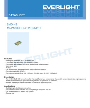
1. Product Overview
This document details the technical specifications for a surface-mount device (SMD) LED emitting brilliant green light. The component is designed for high-density mounting on printed circuit boards (PCBs), offering advantages in miniaturization and automated assembly processes.
1.1 Core Features and Advantages
The LED is supplied on 8mm tape wound on a 7-inch diameter reel, making it compatible with standard automated pick-and-place equipment. It is suitable for both infrared and vapor phase reflow soldering processes. This is a mono-color (single-color) type LED. The product is compliant with environmental regulations: it is lead-free (Pb-free), adheres to the RoHS directive, complies with EU REACH regulations, and meets halogen-free requirements (Bromine <900 ppm, Chlorine <900 ppm, Br+Cl < 1500 ppm).
The compact SMD package enables significant design benefits compared to traditional lead-frame components. These include reduced board space, higher component packing density, minimized storage requirements, and ultimately the potential for smaller end-product equipment. The lightweight nature of the package also makes it ideal for miniature and portable applications.
1.2 Target Applications
This LED is suited for a variety of indicator and backlighting functions, including:
- Dashboard and switch backlighting in automotive or industrial controls.
- Status indicators and keypad backlighting in telecommunication devices such as telephones and fax machines.
- Flat backlighting for liquid crystal displays (LCDs), switches, and symbols.
- General-purpose indicator applications.
2. Technical Specifications
2.1 Device Selection and Material
The LED chip is constructed using Indium Gallium Nitride (InGaN) semiconductor material, which produces a brilliant green emitted color. The encapsulating resin is water clear.
2.2 Absolute Maximum Ratings
The following ratings define the limits beyond which permanent damage to the device may occur. Operation under or at these conditions is not guaranteed.
- Reverse Voltage (VR): 5 V
- Forward Current (IF): 25 mA (Continuous)
- Peak Forward Current (IFP): 100 mA (Duty Cycle 1/10 @ 1 kHz)
- Power Dissipation (Pd): 110 mW
- Electrostatic Discharge (ESD) Human Body Model (HBM): 150 V
- Operating Temperature (Topr): -40°C to +85°C
- Storage Temperature (Tstg): -40°C to +90°C
- Soldering Temperature (Tsol):
- Reflow Soldering: 260°C peak for 10 seconds maximum.
- Hand Soldering: 350°C for 3 seconds maximum.
2.3 Electro-Optical Characteristics
These parameters are specified at an ambient temperature of 25°C and represent typical operating performance.
- Luminous Intensity (Iv): 112 - 285 mcd (measured at IF = 20 mA). Tolerance is ±11%.
- Viewing Angle (2θ1/2): 120 degrees (typical).
- Peak Wavelength (λp): 518 nm (typical).
- Dominant Wavelength (λd): 520 - 535 nm. Tolerance is ±1 nm.
- Spectrum Radiation Bandwidth (Δλ): 20 nm (typical).
- Forward Voltage (VF): 2.75 - 3.95 V (at IF = 20 mA). Tolerance is ±0.05 V.
- Reverse Current (IR): 50 μA maximum (at VR = 5 V).
3. Binning System Explanation
To ensure color and brightness consistency in production, LEDs are sorted into bins based on key parameters. This allows designers to select components matching specific application requirements.
3.1 Luminous Intensity Binning
LEDs are categorized into four bins (R1, R2, S1, S2) based on their measured luminous intensity at 20 mA.
- R1: 112 - 140 mcd
- R2: 140 - 180 mcd
- S1: 180 - 225 mcd
- S2: 225 - 285 mcd
3.2 Dominant Wavelength Binning
The dominant wavelength, which correlates with perceived color, is binned into three groups (X, Y, Z).
- X: 520 - 525 nm
- Y: 525 - 530 nm
- Z: 530 - 535 nm
3.3 Forward Voltage Binning
Forward voltage is binned into four codes (5, 6, 7, 8) within group M. This is important for current-limiting circuit design.
- 5: 2.75 - 3.05 V
- 6: 3.05 - 3.35 V
- 7: 3.35 - 3.65 V
- 8: 3.65 - 3.95 V
4. Performance Curve Analysis
The datasheet provides several characteristic curves that illustrate device behavior under varying conditions. These are crucial for robust circuit design.
4.1 Relative Luminous Intensity vs. Ambient Temperature
This curve shows how light output decreases as the ambient temperature rises. Designers must account for this thermal derating, especially in high-temperature environments or high-power applications, to ensure sufficient brightness is maintained.
4.2 Forward Current Derating Curve
This graph defines the maximum allowable continuous forward current as a function of ambient temperature. As temperature increases, the maximum safe current decreases to prevent overheating and ensure long-term reliability. The absolute maximum of 25 mA is only valid at or below 25°C ambient.
4.3 Luminous Intensity vs. Forward Current
This curve depicts the non-linear relationship between drive current and light output. While increasing current boosts brightness, it also increases power dissipation and junction temperature, impacting efficiency and lifespan.
4.4 Spectrum Distribution
The spectral output curve shows the intensity of light emitted across different wavelengths, centered around the peak wavelength of approximately 518 nm. The narrow bandwidth is characteristic of InGaN-based green LEDs.
4.5 Forward Current vs. Forward Voltage (I-V Curve)
This fundamental curve shows the exponential relationship between voltage and current in a diode. The "knee" voltage is where conduction begins significantly. The slope in the operating region indicates dynamic resistance.
4.6 Radiation Pattern
The polar diagram illustrates the spatial distribution of light intensity. The 120-degree viewing angle indicates a wide, lambertian-like emission pattern suitable for area illumination and wide-viewing indicators.
5. Mechanical and Package Information
5.1 Package Dimensions
The datasheet includes a detailed dimensional drawing of the LED package. Critical dimensions include body length, width, height, and the placement of the cathode/anode terminals. All unspecified tolerances are ±0.1 mm.
5.2 Recommended Solder Pad Layout
A suggested footprint for the PCB is provided to ensure reliable soldering and mechanical stability. The recommended pad dimensions are for reference; designers should modify them based on their specific PCB manufacturing process and thermal requirements.
6. Label and Packaging Information
6.1 Label Explanation
The reel label contains several codes for traceability and identification:
- CPN: Customer's Product Number.
- P/N: Manufacturer's Product Number (e.g., 19-218/GHC-YR1S2M/3T).
- QTY: Packing Quantity.
- CAT: Luminous Intensity Rank (e.g., R1, S2).
- HUE: Chromaticity Coordinates & Dominant Wavelength Rank (e.g., X, Y, Z).
- REF: Forward Voltage Rank (e.g., 5, 6, 7, 8).
- LOT No: Manufacturing Lot Number for traceability.
6.2 Reel and Tape Dimensions
Dimensions for the carrier tape and the 7-inch diameter reel are specified. The standard loaded quantity is 3000 pieces per reel.
6.3 Moisture-Resistant Packaging
The LEDs are packaged in a moisture-barrier bag (aluminum moisture-proof bag) along with a desiccant to absorb ambient humidity. A label on the bag indicates moisture sensitivity level (MSL) and handling instructions. This packaging is critical for components sensitive to moisture-induced damage during reflow soldering ("popcorning").
7. Soldering and Assembly Guidelines
7.1 Critical Precautions
Over-current Protection: LEDs are current-driven devices. An external current-limiting resistor must be used in series. A small change in forward voltage can cause a large change in current, potentially leading to immediate failure (burn-out).
7.2 Storage and Handling
- Do not open the moisture-proof bag until the components are ready for use.
- Before opening: Store at ≤30°C and ≤90% Relative Humidity (RH).
- After opening: The "floor life" (time components can be exposed to ambient factory air) is 1 year at ≤30°C and ≤60% RH. Unused parts should be resealed in a moisture-proof package with desiccant.
- If the desiccant indicator has changed color or the storage time is exceeded, a baking treatment is required: 60 ±5°C for 24 hours.
7.3 Soldering Conditions
Reflow Soldering Profile (Pb-free):
- Pre-heating: 150-200°C for 60-120 seconds.
- Time above liquidus (217°C): 60-150 seconds.
- Peak Temperature: 260°C maximum.
- Time within 5°C of peak: 10 seconds maximum.
- Heating Rate: 3°C/sec maximum (pre-heat to peak).
- Cooling Rate: 6°C/sec maximum.
Hand Soldering: Use a soldering iron with a tip temperature <350°C for no more than 3 seconds per terminal. The iron power should be 25W or less. Allow an interval of at least 2 seconds between soldering each terminal. Hand soldering carries a higher risk of thermal damage.
Repairing: Repair after soldering is not recommended. If unavoidable, use a dual-head soldering iron to simultaneously heat both terminals and lift the component evenly to avoid damaging the solder pads or the LED itself. Verify device functionality after any repair.
8. Application Notes and Design Considerations
8.1 Circuit Design
Always use a series resistor to limit the forward current. Calculate the resistor value using Ohm's Law: R = (Vsupply - VF) / IF. Use the maximum VF from the bin or datasheet to ensure current does not exceed limits under worst-case conditions. Consider the power rating of the resistor (P = IF2 * R). For driving multiple LEDs, a series configuration is preferred for current matching, but requires a higher supply voltage. Parallel configurations require individual current-limiting resistors for each LED to prevent current hogging.
8.2 Thermal Management
Although a small SMD component, thermal management is vital for longevity and stable performance. The derating curves clearly show performance loss with temperature. Ensure adequate PCB copper area (thermal relief pads) to dissipate heat, especially when operating near maximum current ratings or in high ambient temperatures. Avoid placing LEDs near other heat-generating components.
8.3 Optical Integration
The wide 120-degree viewing angle makes this LED suitable for applications requiring broad illumination. For more directed light, external lenses or light guides may be necessary. The water-clear resin provides a neutral base color for applications where the LED might be used with color filters or diffusers.
9. Technical Comparison and Positioning
This InGaN-based green LED offers a typical solution in the SMD indicator LED market. Its key differentiators are its compliance with modern environmental standards (Halogen-Free, REACH) and its specification for Pb-free reflow processes. The provided binning information offers a level of color and brightness consistency important for multi-LED arrays or displays. The combination of a relatively high luminous intensity (up to 285 mcd at 20mA) and a standard SMD footprint makes it a versatile choice for both indicator and low-level backlighting tasks. Designers should compare the forward voltage binning and luminous intensity bins with application-specific requirements for voltage headroom and brightness uniformity.
10. Frequently Asked Questions (FAQ)
Q: What is the purpose of the binning codes?
A: Binning ensures electrical and optical consistency. For example, using LEDs from the same VF bin ensures uniform brightness when driven by a common current-limiting resistor. Using LEDs from the same wavelength bin ensures color matching.
Q: Can I drive this LED without a current-limiting resistor if my power supply is exactly 3.2V?
A: No. The forward voltage has a range (2.75V-3.95V). A supply of 3.2V could cause excessive current in an LED with a low VF, leading to failure. A series resistor is always mandatory for constant-voltage drives.
Q: How do I interpret the "Peak Forward Current" rating of 100mA?
A: This is a pulsed current rating (1/10 duty cycle at 1kHz). It should not be used for continuous operation. The continuous DC current must not exceed 25mA.
Q: Why is moisture-sensitive packaging important?
A> Moisture absorbed into the plastic package can vaporize rapidly during the high-temperature reflow soldering process, causing internal delamination, cracking, or "popcorning," which destroys the component.
11. Design Use Case Example
Scenario: Designing a status indicator panel with 10 uniformly bright green LEDs.
- Current Setting: Choose a drive current. For a balance of brightness and longevity, select IF = 20 mA.
- Voltage Bin Selection: To ensure uniform brightness with a single current-limiting resistor value, specify LEDs from the same forward voltage bin (e.g., Bin 6: 3.05-3.35V). Use the maximum VF from that bin (3.35V) for the worst-case resistor calculation.
- Brightness Bin Selection: Specify the required luminous intensity bin (e.g., S1: 180-225 mcd) to guarantee a minimum brightness level.
- Circuit Design: With a 5V supply (Vsupply), calculate the series resistor: R = (5V - 3.35V) / 0.020A = 82.5Ω. Use the nearest standard value, 82Ω. Resistor power: P = (0.020A)2 * 82Ω = 0.0328W. A standard 1/10W (0.1W) resistor is sufficient.
- Layout: Place the LEDs on the PCB using the recommended pad layout. Connect all LEDs in parallel, each with its own 82Ω series resistor to prevent current imbalance.
- Assembly: Follow the reflow profile guidelines. Store opened reels in a dry cabinet if not used immediately.
12. Operational Principle
This LED is a semiconductor photonic device. Its core is a chip made of InGaN (Indium Gallium Nitride) materials, forming a p-n junction. When a forward voltage exceeding the junction's threshold is applied, electrons and holes are injected across the junction. When these charge carriers recombine, they release energy in the form of photons (light). The specific composition of the InGaN alloy determines the bandgap energy, which directly corresponds to the wavelength (color) of the emitted light—in this case, brilliant green (~518-535 nm). The water-clear epoxy resin encapsulates the chip, providing mechanical protection, shaping the radiation pattern, and acting as a refractive medium.
13. Technology Trends
The development of SMD LEDs like this one is driven by trends in electronics miniaturization, automation, and energy efficiency. There is a continuous push for higher luminous efficacy (more light output per electrical watt), which improves system efficiency and reduces thermal load. Advancements in phosphor technology and chip design are expanding the color gamut and color rendering capabilities of LEDs. Furthermore, integration is a key trend, with multi-chip packages (RGB, white) and even driver ICs being combined into single modules. The emphasis on environmental compliance (Halogen-Free, REACH) and high-reliability manufacturing processes for automotive and industrial applications continues to shape component specifications and testing requirements.
LED Specification Terminology
Complete explanation of LED technical terms
Photoelectric Performance
| Term | Unit/Representation | Simple Explanation | Why Important |
|---|---|---|---|
| Luminous Efficacy | lm/W (lumens per watt) | Light output per watt of electricity, higher means more energy efficient. | Directly determines energy efficiency grade and electricity cost. |
| Luminous Flux | lm (lumens) | Total light emitted by source, commonly called "brightness". | Determines if the light is bright enough. |
| Viewing Angle | ° (degrees), e.g., 120° | Angle where light intensity drops to half, determines beam width. | Affects illumination range and uniformity. |
| CCT (Color Temperature) | K (Kelvin), e.g., 2700K/6500K | Warmth/coolness of light, lower values yellowish/warm, higher whitish/cool. | Determines lighting atmosphere and suitable scenarios. |
| CRI / Ra | Unitless, 0–100 | Ability to render object colors accurately, Ra≥80 is good. | Affects color authenticity, used in high-demand places like malls, museums. |
| SDCM | MacAdam ellipse steps, e.g., "5-step" | Color consistency metric, smaller steps mean more consistent color. | Ensures uniform color across same batch of LEDs. |
| Dominant Wavelength | nm (nanometers), e.g., 620nm (red) | Wavelength corresponding to color of colored LEDs. | Determines hue of red, yellow, green monochrome LEDs. |
| Spectral Distribution | Wavelength vs intensity curve | Shows intensity distribution across wavelengths. | Affects color rendering and quality. |
Electrical Parameters
| Term | Symbol | Simple Explanation | Design Considerations |
|---|---|---|---|
| Forward Voltage | Vf | Minimum voltage to turn on LED, like "starting threshold". | Driver voltage must be ≥Vf, voltages add up for series LEDs. |
| Forward Current | If | Current value for normal LED operation. | Usually constant current drive, current determines brightness & lifespan. |
| Max Pulse Current | Ifp | Peak current tolerable for short periods, used for dimming or flashing. | Pulse width & duty cycle must be strictly controlled to avoid damage. |
| Reverse Voltage | Vr | Max reverse voltage LED can withstand, beyond may cause breakdown. | Circuit must prevent reverse connection or voltage spikes. |
| Thermal Resistance | Rth (°C/W) | Resistance to heat transfer from chip to solder, lower is better. | High thermal resistance requires stronger heat dissipation. |
| ESD Immunity | V (HBM), e.g., 1000V | Ability to withstand electrostatic discharge, higher means less vulnerable. | Anti-static measures needed in production, especially for sensitive LEDs. |
Thermal Management & Reliability
| Term | Key Metric | Simple Explanation | Impact |
|---|---|---|---|
| Junction Temperature | Tj (°C) | Actual operating temperature inside LED chip. | Every 10°C reduction may double lifespan; too high causes light decay, color shift. |
| Lumen Depreciation | L70 / L80 (hours) | Time for brightness to drop to 70% or 80% of initial. | Directly defines LED "service life". |
| Lumen Maintenance | % (e.g., 70%) | Percentage of brightness retained after time. | Indicates brightness retention over long-term use. |
| Color Shift | Δu′v′ or MacAdam ellipse | Degree of color change during use. | Affects color consistency in lighting scenes. |
| Thermal Aging | Material degradation | Deterioration due to long-term high temperature. | May cause brightness drop, color change, or open-circuit failure. |
Packaging & Materials
| Term | Common Types | Simple Explanation | Features & Applications |
|---|---|---|---|
| Package Type | EMC, PPA, Ceramic | Housing material protecting chip, providing optical/thermal interface. | EMC: good heat resistance, low cost; Ceramic: better heat dissipation, longer life. |
| Chip Structure | Front, Flip Chip | Chip electrode arrangement. | Flip chip: better heat dissipation, higher efficacy, for high-power. |
| Phosphor Coating | YAG, Silicate, Nitride | Covers blue chip, converts some to yellow/red, mixes to white. | Different phosphors affect efficacy, CCT, and CRI. |
| Lens/Optics | Flat, Microlens, TIR | Optical structure on surface controlling light distribution. | Determines viewing angle and light distribution curve. |
Quality Control & Binning
| Term | Binning Content | Simple Explanation | Purpose |
|---|---|---|---|
| Luminous Flux Bin | Code e.g., 2G, 2H | Grouped by brightness, each group has min/max lumen values. | Ensures uniform brightness in same batch. |
| Voltage Bin | Code e.g., 6W, 6X | Grouped by forward voltage range. | Facilitates driver matching, improves system efficiency. |
| Color Bin | 5-step MacAdam ellipse | Grouped by color coordinates, ensuring tight range. | Guarantees color consistency, avoids uneven color within fixture. |
| CCT Bin | 2700K, 3000K etc. | Grouped by CCT, each has corresponding coordinate range. | Meets different scene CCT requirements. |
Testing & Certification
| Term | Standard/Test | Simple Explanation | Significance |
|---|---|---|---|
| LM-80 | Lumen maintenance test | Long-term lighting at constant temperature, recording brightness decay. | Used to estimate LED life (with TM-21). |
| TM-21 | Life estimation standard | Estimates life under actual conditions based on LM-80 data. | Provides scientific life prediction. |
| IESNA | Illuminating Engineering Society | Covers optical, electrical, thermal test methods. | Industry-recognized test basis. |
| RoHS / REACH | Environmental certification | Ensures no harmful substances (lead, mercury). | Market access requirement internationally. |
| ENERGY STAR / DLC | Energy efficiency certification | Energy efficiency and performance certification for lighting. | Used in government procurement, subsidy programs, enhances competitiveness. |