Table of Contents
- 1. Product Overview
- 2. Technical Specifications Deep Dive
- 2.1 Absolute Maximum Ratings
- 2.2 Electro-Optical Characteristics
- 3. Binning System Explanation
- 3.1 Luminous Intensity Binning
- 3.2 Dominant Wavelength Binning
- 3.3 Forward Voltage Binning
- 4. Performance Curve Analysis
- 5. Mechanical and Package Information
- 5.1 Package Dimensions
- 5.2 Polarity Identification
- 6. Soldering and Assembly Guidelines
- 6.1 Storage and Moisture Sensitivity
- 6.2 Reflow Soldering Profile
- 6.3 Hand Soldering and Rework
- 7. Packaging and Ordering Information
- 8. Application Recommendations
- 8.1 Typical Application Scenarios
- 8.2 Design Considerations
- 9. Technical Comparison and Differentiation
- 10. Frequently Asked Questions (FAQs)
- 11. Practical Design and Usage Examples
- 12. Operating Principle
- 13. Technology Trends
1. Product Overview
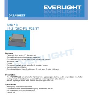
The 17-21/G6C-FN1P2B/3T is a surface-mount device (SMD) LED designed for high-density electronic assemblies. It features a compact footprint, making it ideal for applications where board space is at a premium. The device is constructed using AlGaInP semiconductor material, which produces a brilliant yellow-green light output. This LED is packaged on 8mm tape and supplied on a 7-inch diameter reel, ensuring compatibility with standard automated pick-and-place and reflow soldering equipment used in high-volume manufacturing.
Key advantages of this component include its small size, which enables reduced equipment dimensions and increased packing density on printed circuit boards (PCBs). Its lightweight construction further supports its use in miniature and portable electronic devices. The product is compliant with major environmental and safety standards, including RoHS, REACH, and halogen-free requirements, making it suitable for global markets.
2. Technical Specifications Deep Dive
2.1 Absolute Maximum Ratings
The device is designed to operate reliably within specified limits. Exceeding these ratings may cause permanent damage. The maximum reverse voltage (VR) is 5V. The continuous forward current (IF) should not exceed 25mA, while a peak forward current (IFP) of 60mA is permissible under pulsed conditions (duty cycle 1/10 at 1kHz). The maximum power dissipation (Pd) is 60mW. The component can withstand an electrostatic discharge (ESD) of 2000V per the Human Body Model (HBM). Its operational temperature range is from -40°C to +85°C, with a storage temperature range of -40°C to +90°C.
2.2 Electro-Optical Characteristics
Measured at a standard junction temperature of 25°C and a forward current of 20mA, the LED's performance is characterized by several key parameters. The luminous intensity (Iv) has a typical range defined by its binning system. The viewing angle (2θ1/2) is typically 140 degrees, providing a wide field of illumination. The peak wavelength (λp) is centered around 575nm, while the dominant wavelength (λd) ranges from 570.0nm to 574.5nm. The spectral bandwidth (Δλ) is typically 20nm. The forward voltage (VF) ranges from 1.75V to 2.35V, and the reverse current (IR) is a maximum of 10μA at 5V reverse bias. It is critical to note that the device is not designed for operation under reverse voltage conditions; the VR rating applies only to the IR test.
3. Binning System Explanation
To ensure consistency in application design, the LEDs are sorted into bins based on three key parameters: luminous intensity, dominant wavelength, and forward voltage. This allows designers to select components that meet specific performance criteria for their projects.
3.1 Luminous Intensity Binning
Luminous intensity is categorized into four bins (N1, N2, P1, P2) measured at IF=20mA. The range spans from a minimum of 28.5 mcd (N1 min) to a maximum of 72.0 mcd (P2 max). A tolerance of ±11% applies within each bin.
3.2 Dominant Wavelength Binning
The dominant wavelength, which defines the perceived color, is sorted into three bins (CC2, CC3, CC4). The range is from 570.0nm to 574.5nm, with a tight tolerance of ±1nm to maintain color consistency.
3.3 Forward Voltage Binning
Forward voltage is grouped into three bins (0, 1, 2), ranging from 1.75V to 2.35V at IF=20mA. The tolerance for forward voltage is ±0.1V. Selecting LEDs from the same voltage bin can help ensure uniform brightness when multiple LEDs are driven in parallel.
4. Performance Curve Analysis
The datasheet references typical electro-optical characteristic curves. While specific graphs are not reproduced in text, these curves typically illustrate the relationship between forward current and luminous intensity, forward voltage versus temperature, and the spectral power distribution. Analyzing these curves is essential for understanding the LED's behavior under different operating conditions, such as changes in drive current or ambient temperature, which affect light output and efficiency.
5. Mechanical and Package Information
5.1 Package Dimensions
The LED has a compact SMD package with dimensions of approximately 1.6mm in length, 0.8mm in width, and 0.6mm in height (tolerance ±0.1mm unless otherwise specified). A detailed dimensioned drawing is provided in the datasheet, including pad layout recommendations for PCB design to ensure proper soldering and thermal management.
5.2 Polarity Identification
The cathode is clearly marked on the package. Correct polarity orientation during assembly is crucial for the device to function. The PCB footprint design must align with this marking to prevent reverse installation.
6. Soldering and Assembly Guidelines
Proper handling and soldering are critical to maintaining LED performance and reliability.
6.1 Storage and Moisture Sensitivity
The components are packaged in a moisture-resistant bag with desiccant. The bag should not be opened until the LEDs are ready for use. After opening, unused LEDs should be stored at ≤30°C and ≤60% relative humidity and used within 168 hours (7 days). If this window is exceeded or the desiccant indicates moisture absorption, a baking treatment at 60±5°C for 24 hours is required before use.
6.2 Reflow Soldering Profile
The LED is compatible with infrared and vapor phase reflow processes. For Pb-free soldering, a specific temperature profile must be followed: pre-heating between 150-200°C for 60-120 seconds, time above 217°C (liquidus) for 60-150 seconds, with a peak temperature not exceeding 260°C for a maximum of 10 seconds. The maximum ramp-up rate should be 6°C/sec, and the maximum ramp-down rate 3°C/sec. Reflow soldering should not be performed more than two times.
6.3 Hand Soldering and Rework
If hand soldering is necessary, the soldering iron tip temperature must be below 350°C, applied for no more than 3 seconds per terminal. The iron should have a capacity of less than 25W. A cooling interval of at least 2 seconds should be observed between soldering each terminal. Repair after initial soldering is not recommended. If unavoidable, a specialized double-head soldering iron must be used to simultaneously heat both terminals and avoid mechanical stress on the LED chip.
7. Packaging and Ordering Information
The LEDs are supplied in moisture-resistant packaging. They are loaded into carrier tape with dimensions specified for automated handling. Each reel contains 3000 pieces. The packaging label includes critical information for traceability and selection: Product Number (P/N), quantity (QTY), and the specific bin codes for luminous intensity (CAT), dominant wavelength (HUE), and forward voltage (REF).
8. Application Recommendations
8.1 Typical Application Scenarios
This LED is well-suited for backlighting applications in automotive dashboards and switches, indicator and backlighting in telecommunication devices like phones and fax machines, flat backlighting for LCDs, and general-purpose status indication.
8.2 Design Considerations
Current Limiting: An external current-limiting resistor is mandatory. The LED's exponential I-V characteristic means a small increase in voltage can cause a large, potentially destructive increase in current. The resistor value must be calculated based on the supply voltage and the LED's forward voltage bin.
Thermal Management: While power dissipation is low, ensuring adequate PCB copper area for the pads helps dissipate heat, especially in high ambient temperature environments or when driven at higher currents.
Board Stress: Avoid bending or warping the PCB during or after soldering, as this can induce stress cracks in the LED package.
9. Technical Comparison and Differentiation
Compared to larger lead-frame type LEDs, this SMD variant offers significant space savings, higher placement density, and compatibility with fully automated assembly lines, reducing manufacturing costs. The use of AlGaInP technology provides high efficiency and a saturated yellow-green color. Its compliance with stringent environmental regulations (RoHS, REACH, Halogen-Free) makes it a future-proof choice for modern electronic designs targeting global markets.
10. Frequently Asked Questions (FAQs)
Q: Can I drive this LED without a series resistor?
A: No. The datasheet explicitly warns that a protective resistor must be used. Operating the LED directly from a voltage source will lead to uncontrolled current flow and rapid failure.
Q: What happens if I exceed the 7-day floor life after opening the moisture-proof bag?
A: The LEDs may absorb moisture from the atmosphere. Soldering them without proper baking can cause "popcorning" or internal delamination due to rapid vapor expansion during reflow, leading to failure. Follow the prescribed baking procedure.
Q: How do I interpret the bin codes on the label?
A: The CAT, HUE, and REF codes correspond to the luminous intensity, dominant wavelength, and forward voltage bins detailed in sections 3.1, 3.2, and 3.3. Selecting consistent bins is key for uniform performance in an array.
11. Practical Design and Usage Examples
Example 1: Dashboard Switch Backlighting: A designer needs 10 uniform yellow-green indicators. They should specify LEDs from the same luminous intensity bin (e.g., all P1) and the same dominant wavelength bin (e.g., all CC3) to ensure consistent brightness and color. A single current-limiting resistor can be calculated using the maximum forward voltage from bin 2 (2.35V) to guarantee safe operation for all units, even if some have lower Vf.
Example 2: High-Density Status Panel: For a panel with 50 LEDs, using the SMD package allows a very compact layout. The designer must ensure the PCB pad design matches the datasheet recommendation to facilitate good solder joint formation during reflow. Stencil aperture design should be optimized to prevent solder bridging between the closely spaced pads.
12. Operating Principle
This LED is a semiconductor diode based on Aluminum Gallium Indium Phosphide (AlGaInP) material. When a forward voltage exceeding its bandgap energy is applied, electrons and holes recombine in the active region of the semiconductor, releasing energy in the form of photons. The specific composition of the AlGaInP layers determines the wavelength of the emitted light, which in this case is in the yellow-green spectrum (~575nm). The epoxy resin lens is water-clear to maximize light extraction and shape the emission pattern to a 140-degree viewing angle.
13. Technology Trends
The trend in indicator and backlight LEDs continues toward miniaturization, increased efficiency (lumens per watt), and higher reliability. SMD packages like the 17-21 are becoming standard due to their manufacturing advantages. There is also a growing emphasis on precise binning and tighter tolerances to meet the demands of applications requiring high color and brightness uniformity, such as full-color displays and automotive lighting clusters. Furthermore, the drive for environmentally sustainable electronics ensures that halogen-free and RoHS-compliant materials remain a baseline requirement for all new components.
LED Specification Terminology
Complete explanation of LED technical terms
Photoelectric Performance
| Term | Unit/Representation | Simple Explanation | Why Important |
|---|---|---|---|
| Luminous Efficacy | lm/W (lumens per watt) | Light output per watt of electricity, higher means more energy efficient. | Directly determines energy efficiency grade and electricity cost. |
| Luminous Flux | lm (lumens) | Total light emitted by source, commonly called "brightness". | Determines if the light is bright enough. |
| Viewing Angle | ° (degrees), e.g., 120° | Angle where light intensity drops to half, determines beam width. | Affects illumination range and uniformity. |
| CCT (Color Temperature) | K (Kelvin), e.g., 2700K/6500K | Warmth/coolness of light, lower values yellowish/warm, higher whitish/cool. | Determines lighting atmosphere and suitable scenarios. |
| CRI / Ra | Unitless, 0–100 | Ability to render object colors accurately, Ra≥80 is good. | Affects color authenticity, used in high-demand places like malls, museums. |
| SDCM | MacAdam ellipse steps, e.g., "5-step" | Color consistency metric, smaller steps mean more consistent color. | Ensures uniform color across same batch of LEDs. |
| Dominant Wavelength | nm (nanometers), e.g., 620nm (red) | Wavelength corresponding to color of colored LEDs. | Determines hue of red, yellow, green monochrome LEDs. |
| Spectral Distribution | Wavelength vs intensity curve | Shows intensity distribution across wavelengths. | Affects color rendering and quality. |
Electrical Parameters
| Term | Symbol | Simple Explanation | Design Considerations |
|---|---|---|---|
| Forward Voltage | Vf | Minimum voltage to turn on LED, like "starting threshold". | Driver voltage must be ≥Vf, voltages add up for series LEDs. |
| Forward Current | If | Current value for normal LED operation. | Usually constant current drive, current determines brightness & lifespan. |
| Max Pulse Current | Ifp | Peak current tolerable for short periods, used for dimming or flashing. | Pulse width & duty cycle must be strictly controlled to avoid damage. |
| Reverse Voltage | Vr | Max reverse voltage LED can withstand, beyond may cause breakdown. | Circuit must prevent reverse connection or voltage spikes. |
| Thermal Resistance | Rth (°C/W) | Resistance to heat transfer from chip to solder, lower is better. | High thermal resistance requires stronger heat dissipation. |
| ESD Immunity | V (HBM), e.g., 1000V | Ability to withstand electrostatic discharge, higher means less vulnerable. | Anti-static measures needed in production, especially for sensitive LEDs. |
Thermal Management & Reliability
| Term | Key Metric | Simple Explanation | Impact |
|---|---|---|---|
| Junction Temperature | Tj (°C) | Actual operating temperature inside LED chip. | Every 10°C reduction may double lifespan; too high causes light decay, color shift. |
| Lumen Depreciation | L70 / L80 (hours) | Time for brightness to drop to 70% or 80% of initial. | Directly defines LED "service life". |
| Lumen Maintenance | % (e.g., 70%) | Percentage of brightness retained after time. | Indicates brightness retention over long-term use. |
| Color Shift | Δu′v′ or MacAdam ellipse | Degree of color change during use. | Affects color consistency in lighting scenes. |
| Thermal Aging | Material degradation | Deterioration due to long-term high temperature. | May cause brightness drop, color change, or open-circuit failure. |
Packaging & Materials
| Term | Common Types | Simple Explanation | Features & Applications |
|---|---|---|---|
| Package Type | EMC, PPA, Ceramic | Housing material protecting chip, providing optical/thermal interface. | EMC: good heat resistance, low cost; Ceramic: better heat dissipation, longer life. |
| Chip Structure | Front, Flip Chip | Chip electrode arrangement. | Flip chip: better heat dissipation, higher efficacy, for high-power. |
| Phosphor Coating | YAG, Silicate, Nitride | Covers blue chip, converts some to yellow/red, mixes to white. | Different phosphors affect efficacy, CCT, and CRI. |
| Lens/Optics | Flat, Microlens, TIR | Optical structure on surface controlling light distribution. | Determines viewing angle and light distribution curve. |
Quality Control & Binning
| Term | Binning Content | Simple Explanation | Purpose |
|---|---|---|---|
| Luminous Flux Bin | Code e.g., 2G, 2H | Grouped by brightness, each group has min/max lumen values. | Ensures uniform brightness in same batch. |
| Voltage Bin | Code e.g., 6W, 6X | Grouped by forward voltage range. | Facilitates driver matching, improves system efficiency. |
| Color Bin | 5-step MacAdam ellipse | Grouped by color coordinates, ensuring tight range. | Guarantees color consistency, avoids uneven color within fixture. |
| CCT Bin | 2700K, 3000K etc. | Grouped by CCT, each has corresponding coordinate range. | Meets different scene CCT requirements. |
Testing & Certification
| Term | Standard/Test | Simple Explanation | Significance |
|---|---|---|---|
| LM-80 | Lumen maintenance test | Long-term lighting at constant temperature, recording brightness decay. | Used to estimate LED life (with TM-21). |
| TM-21 | Life estimation standard | Estimates life under actual conditions based on LM-80 data. | Provides scientific life prediction. |
| IESNA | Illuminating Engineering Society | Covers optical, electrical, thermal test methods. | Industry-recognized test basis. |
| RoHS / REACH | Environmental certification | Ensures no harmful substances (lead, mercury). | Market access requirement internationally. |
| ENERGY STAR / DLC | Energy efficiency certification | Energy efficiency and performance certification for lighting. | Used in government procurement, subsidy programs, enhances competitiveness. |