Table of Contents
- 1. Product Overview
- 1.1 Core Advantages and Product Positioning
- 1.2 Target Market and Applications
- 2. Technical Parameter Deep Dive
- 2.1 Absolute Maximum Ratings
- 2.2 Electro-Optical Characteristics
- 2.3 Thermal Considerations
- 3. Binning System Explanation
- 3.1 Luminous Intensity Binning
- 3.2 Dominant Wavelength Binning
- 3.3 Forward Voltage Binning
- 4. Performance Curve Analysis
- 4.1 Spectral Distribution
- 4.2 Radiation Pattern
- 4.3 Forward Current vs. Forward Voltage (I-V Curve)
- 4.4 Relative Luminous Intensity vs. Forward Current
- 4.5 Relative Luminous Intensity vs. Ambient Temperature
- 5. Mechanical and Package Information
- 5.1 Package Dimensions
- 5.2 Polarity Identification
- 6. Soldering and Assembly Guidelines
- 6.1 Current Limiting
- 6.2 Moisture Sensitivity and Storage
- 6.3 Reflow Soldering Profile
- 6.4 Hand Soldering and Rework
- 7. Packaging and Ordering Information
- 7.1 Packaging Specifications
- 7.2 Reel and Label Details
- 8. Application Notes and Design Considerations
- 8.1 Circuit Design
- 8.2 Thermal Management
- 8.3 Optical Integration
- 9. Compliance and Material Information
- 10. Technical Comparison and Differentiation
- 11. Frequently Asked Questions (Based on Technical Parameters)
- 11.1 What resistor value should I use with a 5V supply?
- 11.2 Can I drive this LED without a current-limiting resistor if my supply voltage matches VF?
- 11.3 Why is the storage time after opening the bag limited to 7 days?
- 11.4 How do I interpret the bin codes (e.g., Q2, E4) on the label?
- 12. Practical Design and Usage Examples
- 12.1 Dashboard Switch Backlighting
- 12.2 Status Indicator on a Network Device
- 13. Operating Principle
- 14. Technology Trends
1. Product Overview
This document details the specifications for a compact, high-performance Surface Mount Device (SMD) LED. The component is designed for modern electronic assembly processes, offering a balance of luminous output, reliability, and ease of integration in space-constrained applications.
1.1 Core Advantages and Product Positioning
The primary advantage of this LED is its miniature footprint, which enables significant reductions in printed circuit board (PCB) size and allows for higher component packing density. This leads to more compact end-product designs. The component is lightweight, making it particularly suitable for portable and miniature electronic devices. It is presented on 8mm tape wound on a 7-inch diameter reel, ensuring compatibility with standard automated pick-and-place equipment used in high-volume manufacturing.
1.2 Target Market and Applications
This LED is versatile and targets several key application areas. Its primary use is in backlighting, specifically for instrument panel dashboards, switches, and symbols. It is also well-suited for telecommunication equipment, serving as status indicators and backlights in devices like telephones and fax machines. Furthermore, it can be used for flat backlighting in small LCD panels and for general-purpose indicator applications where a reddish-orange signal is required.
2. Technical Parameter Deep Dive
This section provides a detailed, objective analysis of the LED's key electrical, optical, and thermal parameters as defined under standard test conditions (Ta=25°C).
2.1 Absolute Maximum Ratings
The Absolute Maximum Ratings define the stress limits beyond which permanent damage to the device may occur. These are not intended for normal operation.
- Reverse Voltage (VR): 5 V. Exceeding this voltage in reverse bias can cause junction breakdown.
- Continuous Forward Current (IF): 25 mA. The maximum DC current for reliable long-term operation.
- Peak Forward Current (IFP): 60 mA (Duty Cycle 1/10 @ 1kHz). This rating allows for short pulses of higher current, useful for multiplexing or pulsed operation schemes.
- Power Dissipation (Pd): 60 mW. The maximum amount of power the device can dissipate as heat without exceeding its thermal limits.
- Electrostatic Discharge (ESD) Human Body Model (HBM): 2000 V. This indicates a moderate level of ESD robustness; proper handling procedures are still recommended.
- Operating Temperature (Topr): -40°C to +85°C. The ambient temperature range over which the device is specified to function.
- Storage Temperature (Tstg): -40°C to +90°C.
- Soldering Temperature: The device can withstand reflow soldering with a peak temperature of 260°C for up to 10 seconds, or hand soldering at 350°C for up to 3 seconds per terminal.
2.2 Electro-Optical Characteristics
These parameters define the LED's performance under typical operating conditions (IF=20mA, Ta=25°C).
- Luminous Intensity (Iv): 45.0 mcd (Min), 112.0 mcd (Max). The typical value falls within this wide range, which is managed through a binning system (see Section 3). The viewing angle (2θ1/2) is typically 130 degrees, providing a wide, diffuse emission pattern.
- Spectral Characteristics:
- Peak Wavelength (λp): Typically 621 nm.
- Dominant Wavelength (λd): 605.5 nm (Min), 625.5 nm (Max). This is the wavelength perceived by the human eye and is also subject to binning.
- Spectral Bandwidth (Δλ): Typically 18 nm, defining the purity of the color.
- Electrical Characteristics:
- Forward Voltage (VF): 1.70 V (Min), 2.00 V (Typ), 2.40 V (Max) at IF=20mA. This relatively low voltage is characteristic of AlGaInP material technology.
- Reverse Current (IR): 10 μA (Max) at VR=5V. A critical note specifies that the device is not designed for operation in reverse bias; this test parameter is for leakage characterization only.
2.3 Thermal Considerations
LED performance is highly temperature-dependent. The forward current derating curve is essential for design. As the ambient temperature (Ta) increases above 25°C, the maximum allowable continuous forward current must be reduced linearly to prevent overheating and accelerated degradation. The derating curve provides the specific relationship, ensuring the junction temperature remains within safe limits.
3. Binning System Explanation
To ensure consistency in mass production, LEDs are sorted (binned) based on key parameters. This allows designers to select parts that meet specific application requirements for brightness and color.
3.1 Luminous Intensity Binning
The luminous output is categorized into four bins (P1, P2, Q1, Q2), each covering a specific range from 45.0 mcd to 112.0 mcd. For example, bin Q2 contains LEDs with intensity between 90.0 and 112.0 mcd. A tolerance of ±11% applies within each bin.
3.2 Dominant Wavelength Binning
The color (dominant wavelength) is sorted into five bins (E1 through E5), spanning from 605.5 nm to 625.5 nm in approximately 4nm steps. Bin E4, for instance, covers 617.5 to 621.5 nm. A tighter tolerance of ±1nm is maintained within each wavelength bin.
3.3 Forward Voltage Binning
The datasheet notes a forward voltage tolerance of ±0.1V, though a specific binning table for VF is not provided in the excerpt. This tight tolerance aids in designing consistent current drive circuits.
4. Performance Curve Analysis
Graphical data provides deeper insight into the LED's behavior under varying conditions.
4.1 Spectral Distribution
The spectrum curve shows a single, well-defined peak centered around 621 nm, confirming the reddish-orange emission from the AlGaInP chip material. The narrow bandwidth indicates good color saturation.
4.2 Radiation Pattern
The polar diagram illustrates the spatial distribution of light. The typical 130-degree viewing angle is confirmed, showing a near-Lambertian (cosine) emission pattern where intensity is highest at 0 degrees (perpendicular to the chip) and decreases gradually towards the sides.
4.3 Forward Current vs. Forward Voltage (I-V Curve)
This curve shows the exponential relationship typical of a diode. The voltage rises sharply at very low currents and then increases more linearly in the normal operating range (around 2.0V at 20mA).
4.4 Relative Luminous Intensity vs. Forward Current
This graph demonstrates that light output is approximately proportional to forward current in the operating range, though efficiency may drop slightly at very high currents due to increased heat.
4.5 Relative Luminous Intensity vs. Ambient Temperature
This is a critical curve showing thermal quenching. As ambient temperature increases, the luminous intensity decreases. The output can drop significantly as temperature approaches the maximum operating limit, a key factor for designs in hot environments.
5. Mechanical and Package Information
5.1 Package Dimensions
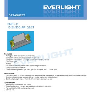
The LED conforms to the "15-21" SMD package outline. Detailed dimensional drawings specify the length, width, height, and lead positions with a standard tolerance of ±0.1mm unless otherwise noted. This information is crucial for PCB footprint design and clearance checks.
5.2 Polarity Identification
A clear cathode mark is indicated on the package, essential for correct orientation during assembly. Installing the LED in reverse polarity will prevent it from illuminating and may subject it to reverse voltage stress.
6. Soldering and Assembly Guidelines
Proper handling is vital for reliability.
6.1 Current Limiting
An external current-limiting resistor is mandatory. The LED's exponential I-V characteristic means a small increase in voltage can cause a large, potentially destructive increase in current. The resistor sets the operating point.
6.2 Moisture Sensitivity and Storage
The components are packaged in a moisture-resistant barrier bag with desiccant. The bag should not be opened until the parts are ready for use. After opening, unused LEDs must be stored in conditions of 30°C/60%RH or less and used within 168 hours (7 days). If exceeded, a bake-out at 60±5°C for 24 hours is required before reflow to prevent "popcorning" damage during soldering.
6.3 Reflow Soldering Profile
A detailed Pb-free reflow profile is provided:
- Pre-heating: 150-200°C for 60-120 seconds.
- Time Above Liquidus (217°C): 60-150 seconds.
- Peak Temperature: 260°C maximum, held for no more than 10 seconds.
- Heating/Cooling Rates: Maximum 6°C/sec and 3°C/sec, respectively.
6.4 Hand Soldering and Rework
If hand soldering is necessary, the iron tip temperature must be below 350°C, applied for no more than 3 seconds per terminal, using a low-power iron (<25W). A cooling interval of >2 seconds between terminals is required. Rework is strongly discouraged. If unavoidable, a specialized double-head soldering iron must be used to simultaneously heat both terminals, preventing mechanical stress on the solder joints. The potential for thermal damage during rework must be evaluated beforehand.
7. Packaging and Ordering Information
7.1 Packaging Specifications
The LEDs are supplied in embossed carrier tape with dimensions specified for the pockets and sprocket holes. The tape is wound onto a standard 7-inch (178mm) diameter reel. Each reel contains 2000 pieces.
7.2 Reel and Label Details
Dimensions for the empty reel are provided. The reel label contains critical information:
- Customer Part Number (CPN)
- Manufacturer Part Number (P/N): 15-21/S3C-AP1Q2/2T
- Packing Quantity (QTY)
- Luminous Intensity Rank (CAT)
- Chromaticity/Dominant Wavelength Rank (HUE)
- Forward Voltage Rank (REF)
- Lot Number (LOT No.)
8. Application Notes and Design Considerations
8.1 Circuit Design
Always use a series resistor to set the forward current. Calculate the resistor value using R = (Vsupply - VF) / IF, where VF should be taken as the maximum value (2.4V) from the datasheet to ensure the current does not exceed the limit under worst-case conditions. Consider the power rating of the resistor (P = IF2 * R).
8.2 Thermal Management
While the package is small, effective heat sinking through the PCB is important for maintaining brightness and longevity, especially in high-ambient-temperature environments or when driving near the maximum current. Use the derating curve to determine the safe operating current for your application's maximum expected ambient temperature. Ensure adequate copper area around the LED pads on the PCB to act as a heat spreader.
8.3 Optical Integration
The wide 130-degree viewing angle makes this LED suitable for applications requiring broad, even illumination without secondary optics. For more directed light, external lenses or light guides may be necessary. The water-clear resin ensures minimal light absorption within the package itself.
9. Compliance and Material Information
The product is compliant with several key environmental and safety directives, which is a significant advantage for modern electronics manufacturing. It is confirmed to be Pb-free (lead-free), aligning with the Restriction of Hazardous Substances (RoHS) directive. It also complies with the EU's REACH regulation concerning chemical substances. Furthermore, it meets halogen-free requirements, with Bromine (Br) and Chlorine (Cl) content each below 900 ppm, and their sum below 1500 ppm, reducing environmental impact during disposal.
10. Technical Comparison and Differentiation
Compared to traditional through-hole or larger SMD LEDs, the key differentiator of this 15-21 package is its exceptional miniaturization, enabling next-generation compact designs. The use of AlGaInP semiconductor material provides efficient reddish-orange light with good color stability over temperature and lifetime, often superior to older technologies like GaAsP. The combination of a wide viewing angle, robust SMT compatibility, and full environmental compliance makes it a modern, reliable choice for cost-sensitive, high-volume applications where board space is at a premium.
11. Frequently Asked Questions (Based on Technical Parameters)
11.1 What resistor value should I use with a 5V supply?
Using the maximum VF of 2.4V and a target IF of 20mA: R = (5V - 2.4V) / 0.020A = 130 Ohms. The nearest standard value of 130Ω or 150Ω would be suitable. The resistor power dissipation would be P = (0.020)2 * 130 = 0.052W, so a standard 1/8W (0.125W) resistor is sufficient.
11.2 Can I drive this LED without a current-limiting resistor if my supply voltage matches VF?
No. This is strongly discouraged. The forward voltage has a tolerance (1.7V to 2.4V) and varies with temperature. A supply voltage fixed at, say, 2.0V could cause excessive current in an LED with a low VF, leading to rapid failure. A series resistor is essential for stable, safe operation.
11.3 Why is the storage time after opening the bag limited to 7 days?
SMD packages can absorb moisture from the air. During the high-temperature reflow soldering process, this trapped moisture can vaporize rapidly, creating internal pressure that can delaminate the package or crack the die ("popcorning"). The 7-day limit and baking procedure are critical quality controls to prevent this failure mode.
11.4 How do I interpret the bin codes (e.g., Q2, E4) on the label?
The bin codes tell you the performance group of the LEDs on that reel. "Q2" indicates high-brightness LEDs (90-112 mcd). "E4" indicates a dominant wavelength in the 617.5-621.5 nm range. Using parts from the same bin ensures consistency in brightness and color across your product.
12. Practical Design and Usage Examples
12.1 Dashboard Switch Backlighting
In an automotive dashboard, multiple switches require uniform, reliable backlighting. Several of these LEDs can be placed behind a translucent switch cap. Their wide viewing angle ensures even illumination across the switch surface. The low operating voltage allows them to be driven directly from the vehicle's regulated 5V or 3.3V systems with simple resistor networks. The high-temperature operating range (-40°C to +85°C) is suitable for the automotive environment.
12.2 Status Indicator on a Network Device
For a "link activity" or "power" indicator on a router or modem, a single LED provides a clear visual signal. The reddish-orange color is highly visible. The component can be driven by a GPIO pin from a microcontroller. A series resistor is connected between the GPIO and the LED anode, with the cathode connected to ground. The microcontroller firmware can toggle the pin to create steady or blinking patterns. The SMD format allows for a very low-profile design on the front panel PCB.
13. Operating Principle
This LED is based on a semiconductor chip made from Aluminum Gallium Indium Phosphide (AlGaInP). When a forward voltage is applied, electrons and holes are injected into the active region of the semiconductor junction. When these charge carriers recombine, they release energy in the form of photons (light). The specific composition of the AlGaInP alloy determines the bandgap energy, which in turn defines the wavelength (color) of the emitted light—in this case, in the reddish-orange spectrum (605-625 nm). The light generated within the chip is extracted through the top surface and shaped by the water-clear epoxy resin lens of the package.
14. Technology Trends
The general trend in indicator and backlight LED technology continues toward higher efficiency (more light output per unit of electrical power), increased miniaturization beyond packages like the 15-21, and broader color gamuts. There is also a strong focus on enhancing reliability and longevity under harsh conditions, such as higher temperature and humidity. Integration of control electronics, such as constant-current drivers or pulse-width modulation (PWM) controllers, directly into the LED package is another evolving trend, simplifying circuit design for the end user. Furthermore, the drive for sustainability keeps pushing advancements in materials to meet ever-stricter environmental regulations beyond RoHS and REACH.
LED Specification Terminology
Complete explanation of LED technical terms
Photoelectric Performance
| Term | Unit/Representation | Simple Explanation | Why Important |
|---|---|---|---|
| Luminous Efficacy | lm/W (lumens per watt) | Light output per watt of electricity, higher means more energy efficient. | Directly determines energy efficiency grade and electricity cost. |
| Luminous Flux | lm (lumens) | Total light emitted by source, commonly called "brightness". | Determines if the light is bright enough. |
| Viewing Angle | ° (degrees), e.g., 120° | Angle where light intensity drops to half, determines beam width. | Affects illumination range and uniformity. |
| CCT (Color Temperature) | K (Kelvin), e.g., 2700K/6500K | Warmth/coolness of light, lower values yellowish/warm, higher whitish/cool. | Determines lighting atmosphere and suitable scenarios. |
| CRI / Ra | Unitless, 0–100 | Ability to render object colors accurately, Ra≥80 is good. | Affects color authenticity, used in high-demand places like malls, museums. |
| SDCM | MacAdam ellipse steps, e.g., "5-step" | Color consistency metric, smaller steps mean more consistent color. | Ensures uniform color across same batch of LEDs. |
| Dominant Wavelength | nm (nanometers), e.g., 620nm (red) | Wavelength corresponding to color of colored LEDs. | Determines hue of red, yellow, green monochrome LEDs. |
| Spectral Distribution | Wavelength vs intensity curve | Shows intensity distribution across wavelengths. | Affects color rendering and quality. |
Electrical Parameters
| Term | Symbol | Simple Explanation | Design Considerations |
|---|---|---|---|
| Forward Voltage | Vf | Minimum voltage to turn on LED, like "starting threshold". | Driver voltage must be ≥Vf, voltages add up for series LEDs. |
| Forward Current | If | Current value for normal LED operation. | Usually constant current drive, current determines brightness & lifespan. |
| Max Pulse Current | Ifp | Peak current tolerable for short periods, used for dimming or flashing. | Pulse width & duty cycle must be strictly controlled to avoid damage. |
| Reverse Voltage | Vr | Max reverse voltage LED can withstand, beyond may cause breakdown. | Circuit must prevent reverse connection or voltage spikes. |
| Thermal Resistance | Rth (°C/W) | Resistance to heat transfer from chip to solder, lower is better. | High thermal resistance requires stronger heat dissipation. |
| ESD Immunity | V (HBM), e.g., 1000V | Ability to withstand electrostatic discharge, higher means less vulnerable. | Anti-static measures needed in production, especially for sensitive LEDs. |
Thermal Management & Reliability
| Term | Key Metric | Simple Explanation | Impact |
|---|---|---|---|
| Junction Temperature | Tj (°C) | Actual operating temperature inside LED chip. | Every 10°C reduction may double lifespan; too high causes light decay, color shift. |
| Lumen Depreciation | L70 / L80 (hours) | Time for brightness to drop to 70% or 80% of initial. | Directly defines LED "service life". |
| Lumen Maintenance | % (e.g., 70%) | Percentage of brightness retained after time. | Indicates brightness retention over long-term use. |
| Color Shift | Δu′v′ or MacAdam ellipse | Degree of color change during use. | Affects color consistency in lighting scenes. |
| Thermal Aging | Material degradation | Deterioration due to long-term high temperature. | May cause brightness drop, color change, or open-circuit failure. |
Packaging & Materials
| Term | Common Types | Simple Explanation | Features & Applications |
|---|---|---|---|
| Package Type | EMC, PPA, Ceramic | Housing material protecting chip, providing optical/thermal interface. | EMC: good heat resistance, low cost; Ceramic: better heat dissipation, longer life. |
| Chip Structure | Front, Flip Chip | Chip electrode arrangement. | Flip chip: better heat dissipation, higher efficacy, for high-power. |
| Phosphor Coating | YAG, Silicate, Nitride | Covers blue chip, converts some to yellow/red, mixes to white. | Different phosphors affect efficacy, CCT, and CRI. |
| Lens/Optics | Flat, Microlens, TIR | Optical structure on surface controlling light distribution. | Determines viewing angle and light distribution curve. |
Quality Control & Binning
| Term | Binning Content | Simple Explanation | Purpose |
|---|---|---|---|
| Luminous Flux Bin | Code e.g., 2G, 2H | Grouped by brightness, each group has min/max lumen values. | Ensures uniform brightness in same batch. |
| Voltage Bin | Code e.g., 6W, 6X | Grouped by forward voltage range. | Facilitates driver matching, improves system efficiency. |
| Color Bin | 5-step MacAdam ellipse | Grouped by color coordinates, ensuring tight range. | Guarantees color consistency, avoids uneven color within fixture. |
| CCT Bin | 2700K, 3000K etc. | Grouped by CCT, each has corresponding coordinate range. | Meets different scene CCT requirements. |
Testing & Certification
| Term | Standard/Test | Simple Explanation | Significance |
|---|---|---|---|
| LM-80 | Lumen maintenance test | Long-term lighting at constant temperature, recording brightness decay. | Used to estimate LED life (with TM-21). |
| TM-21 | Life estimation standard | Estimates life under actual conditions based on LM-80 data. | Provides scientific life prediction. |
| IESNA | Illuminating Engineering Society | Covers optical, electrical, thermal test methods. | Industry-recognized test basis. |
| RoHS / REACH | Environmental certification | Ensures no harmful substances (lead, mercury). | Market access requirement internationally. |
| ENERGY STAR / DLC | Energy efficiency certification | Energy efficiency and performance certification for lighting. | Used in government procurement, subsidy programs, enhances competitiveness. |