Table of Contents
- 1. Product Overview
- 2. Technical Parameter Deep-Dive
- 2.1 Absolute Maximum Ratings
- 2.2 Electro-Optical Characteristics
- 3. Binning System Explanation
- 3.1 Luminous Intensity Binning
- 4. Performance Curve Analysis
- 4.1 Inferred Curve Characteristics
- 5. Mechanical and Package Information
- 5.1 Package Dimensions
- 6. Soldering and Assembly Guidelines
- 6.1 Critical Precautions
- 6.2 Soldering Profile (Pb-free)
- 6.3 Hand Soldering & Repair
- 7. Packaging and Ordering Information
- 7.1 Packaging Specifications
- 7.2 Label Explanation
- 8. Application Suggestions
- 8.1 Typical Application Scenarios
- 8.2 Design Considerations
- 9. Technical Comparison & Differentiation
- 10. Frequently Asked Questions (Based on Technical Parameters)
- 10.1 Why is a current-limiting resistor absolutely necessary?
- 10.2 What does the "±11% tolerance" on luminous intensity mean for my design?
- 10.3 Can I use this LED outdoors?
- 10.4 How do I interpret the bin codes (P, Q, N) when ordering?
- 11. Practical Design Case Study
- 12. Operating Principle Introduction
- 13. Technology Trends
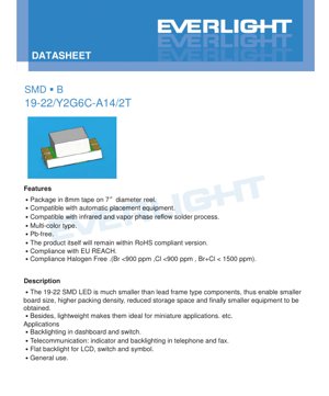
1. Product Overview
The 19-22/Y2G6C-A14/2T is a compact, surface-mount LED designed for high-density applications. It represents a significant advancement over traditional lead-frame type components, enabling substantial reductions in board size, storage space, and overall equipment dimensions. Its lightweight construction makes it particularly suitable for miniature and space-constrained applications.
The core advantage of this product lies in its efficient use of board real estate and its compatibility with modern, automated manufacturing processes. It is supplied in industry-standard 8mm tape on 7-inch diameter reels, facilitating seamless integration with automated pick-and-place equipment. The device is engineered for reliability and environmental compliance, being Pb-free, RoHS compliant, and adhering to EU REACH and stringent halogen-free standards (Br <900 ppm, Cl <900 ppm, Br+Cl < 1500 ppm).
2. Technical Parameter Deep-Dive
2.1 Absolute Maximum Ratings
These ratings define the limits beyond which permanent damage to the device may occur. Operation under these conditions is not guaranteed.
- Reverse Voltage (VR): 5V. Exceeding this voltage in reverse bias can cause junction breakdown.
- Forward Current (IF): 25 mA (continuous) for both Y2 (Brilliant Yellow) and G6 (Brilliant Yellow-Green) chip types.
- Peak Forward Current (IFP): 60 mA, permissible under pulsed conditions (duty cycle 1/10 @ 1kHz).
- Power Dissipation (Pd): 60 mW. This is the maximum power the package can dissipate without exceeding its thermal limits.
- Operating Temperature (Topr): -40°C to +85°C. The device is rated for industrial temperature ranges.
- Storage Temperature (Tstg): -40°C to +90°C.
- Electrostatic Discharge (ESD) HBM: 2000V. This Class 1B ESD rating indicates moderate sensitivity; proper ESD handling procedures are recommended.
- Soldering Temperature (Tsol): Reflow: 260°C max for 10 seconds. Hand soldering: 350°C max for 3 seconds per terminal.
2.2 Electro-Optical Characteristics
Measured at a standard test condition of Ta = 25°C and IF = 20mA, unless otherwise specified. The ±11% tolerance on luminous intensity is a critical design consideration.
- Luminous Intensity (Iv):
- Y2 (Brilliant Yellow): Typical value is provided within a binning range of 45.0-112 mcd.
- G6 (Brilliant Yellow-Green): Typical value is provided within a binning range of 28.5-72.0 mcd.
- Viewing Angle (2θ1/2): 130 degrees (typical). This wide viewing angle is suitable for indicator and backlighting applications requiring broad visibility.
- Peak Wavelength (λp):
- Y2: 591 nm (typical).
- G6: 575 nm (typical).
- Dominant Wavelength (λd):
- Y2: 589 nm (typical).
- G6: 573 nm (typical).
- Spectral Bandwidth (Δλ):
- Y2: 15 nm (typical).
- G6: 20 nm (typical). The slightly broader spectrum of the G6 chip is characteristic of its material composition.
- Forward Voltage (VF):
- Y2 & G6: 2.00V (typical), with a range from 1.70V to 2.40V at IF=20mA. This relatively low VF contributes to higher efficiency.
- Reverse Current (IR): 10 μA (max) at VR=5V.
3. Binning System Explanation
The luminous output of LEDs varies from batch to batch. A binning system ensures consistency for the end-user by grouping LEDs with similar performance.
3.1 Luminous Intensity Binning
For Y2 (Brilliant Yellow):
- Bin Code P: 45.0 mcd (Min) to 72.0 mcd (Max).
- Bin Code Q: 72.0 mcd (Min) to 112 mcd (Max).
For G6 (Brilliant Yellow-Green):
- Bin Code N: 28.5 mcd (Min) to 45.0 mcd (Max).
- Bin Code P: 45.0 mcd (Min) to 72.0 mcd (Max).
The specific bin code (CAT) is indicated on the product label. Designers must account for the minimum value within a selected bin to guarantee sufficient brightness in their application.
4. Performance Curve Analysis
While specific graphical data points are not provided in the text extract, the datasheet references typical electro-optical characteristic curves for both the Y2 and G6 chip types. These curves are essential for understanding device behavior under non-standard conditions.
4.1 Inferred Curve Characteristics
Based on standard LED physics and the parameters provided, the following relationships are expected:
- Relative Luminous Intensity vs. Forward Current (IF): The light output will increase super-linearly with current up to a point, after which efficiency droop may occur. Operation should be kept at or below the rated IF of 25mA.
- Relative Luminous Intensity vs. Ambient Temperature (Ta): Luminous intensity typically decreases as junction temperature rises. The curve will show a negative slope, emphasizing the importance of thermal management for maintaining consistent brightness, especially at high ambient temperatures.
- Forward Voltage vs. Forward Current (VF-IF): This will exhibit the classic diode exponential curve. The typical VF of 2.0V at 20mA is a key point on this curve.
- Forward Current vs. Ambient Temperature: This derating curve likely shows the maximum permissible IF decreasing as Ta increases to prevent exceeding the Pd limit.
- Spectral Distribution: The curves for both chips will show a distinct peak at their respective λp (591nm for Y2, 575nm for G6) with the specified bandwidth (Δλ).
5. Mechanical and Package Information
5.1 Package Dimensions
The 19-22 SMD LED features an industry-standard package footprint. Key dimensions (tolerance ±0.1mm unless noted) include a compact body size critical for high-density layouts. The exact length, width, and height are defined in the detailed dimension drawing, which includes pad layout, component outline, and polarity identification (typically via a cathode mark or a cut corner on the package).
6. Soldering and Assembly Guidelines
6.1 Critical Precautions
- Current Limiting: An external series resistor is mandatory to prevent thermal runaway and burnout due to the LED's negative temperature coefficient and sharp I-V characteristics.
- Storage & Moisture Sensitivity:
- Do not open the moisture-proof bag until ready for use.
- After opening, unused LEDs must be stored at ≤30°C and ≤60% RH.
- The "floor life" after bag opening is 168 hours (7 days).
- If exceeded, a bake-out at 60±5°C for 24 hours is required before reflow.
6.2 Soldering Profile (Pb-free)
A recommended reflow profile is provided:
- Pre-heating: 150-200°C for 60-120 seconds.
- Time Above Liquidus (217°C): 60-150 seconds.
- Peak Temperature: 260°C maximum, held for a maximum of 10 seconds.
- Heating Rate: Maximum 6°C/sec.
- Time Above 255°C: Maximum 30 seconds.
- Cooling Rate: Maximum 3°C/sec.
Important Restrictions: Reflow soldering should not be performed more than two times. Avoid mechanical stress on the LED during heating and do not warp the PCB after soldering.
6.3 Hand Soldering & Repair
If hand soldering is unavoidable:
- Use a soldering iron with a tip temperature <350°C for <3 seconds per terminal.
- Iron power should be ≤25W.
- Allow a 2-second minimum interval between soldering each terminal.
- Repair is strongly discouraged. If absolutely necessary, use a double-head soldering iron to simultaneously heat both terminals and lift the component to avoid pad damage. Verify device functionality post-repair.
7. Packaging and Ordering Information
7.1 Packaging Specifications
- Carrier Tape: 8mm width, loaded onto 7-inch diameter reels.
- Quantity per Reel: 2000 pieces.
- Moisture-Resistant Packaging: Includes a desiccant and is sealed in an aluminum moisture-proof bag.
7.2 Label Explanation
The reel label contains critical information for traceability and correct application:
- CPN: Customer's Part Number.
- P/N: Manufacturer's Part Number (e.g., 19-22/Y2G6C-A14/2T).
- QTY: Packing quantity.
- CAT: Luminous Intensity Rank (Bin Code: e.g., P, Q, N).
- HUE: Chromaticity Coordinates & Dominant Wavelength Rank.
- REF: Forward Voltage Rank.
- LOT No: Manufacturing Lot Number for traceability.
8. Application Suggestions
8.1 Typical Application Scenarios
- Automotive Interior: Backlighting for dashboard instruments, switches, and control panels.
- Telecommunications Equipment: Status indicators and keypad backlighting in telephones, fax machines, and routers.
- Consumer Electronics: Flat backlighting for small LCD displays, switch illumination, and symbolic icons.
- General Indicator Use: Power status, mode indication, and alert signals in a wide variety of electronic devices.
8.2 Design Considerations
- Current Drive Circuit: Always implement a constant-current circuit or a voltage source with a series current-limiting resistor. Calculate the resistor value using R = (Vsupply - VF) / IF, using the maximum VF from the datasheet to ensure IF does not exceed the limit under worst-case conditions.
- Thermal Management: While the power dissipation is low, ensure adequate PCB copper area or thermal vias under the LED pads if operating at high ambient temperatures or at maximum IF to maintain performance and longevity.
- Optical Design: The 130-degree viewing angle provides wide emission. For focused or directed light, external lenses or light guides may be necessary.
9. Technical Comparison & Differentiation
The primary differentiators of the 19-22 series are its miniature size and comprehensive environmental compliance. Compared to larger SMD LEDs or through-hole variants, it enables superior packing density. Its specific AlGaInP material system for yellow and yellow-green colors offers high efficiency and color purity in these wavelengths. The combination of RoHS, REACH, and halogen-free compliance makes it suitable for the most demanding global markets and environmentally conscious designs, often providing an advantage over older or less compliant components.
10. Frequently Asked Questions (Based on Technical Parameters)
10.1 Why is a current-limiting resistor absolutely necessary?
The forward voltage (VF) of an LED has a negative temperature coefficient and varies from unit to unit (1.7V to 2.4V). Connecting it directly to a voltage source even slightly above its VF will cause current to rise exponentially, quickly exceeding the Absolute Maximum Rating of 25mA and leading to immediate thermal destruction. The resistor provides a linear, stable current limit.
10.2 What does the "±11% tolerance" on luminous intensity mean for my design?
It means the actual luminous intensity of any single LED can be up to 11% higher or lower than the typical or binned value. Therefore, your optical system should be designed to function correctly with the minimum expected intensity (Typical/Bin Min * 0.89). Do not design based solely on the typical value.
10.3 Can I use this LED outdoors?
The operating temperature range is -40°C to +85°C, which covers many outdoor environments. However, direct exposure to UV radiation, moisture, and contaminants is not addressed by the chip package alone. For outdoor use, the LED must be properly potted or housed within an enclosure that provides environmental sealing and protection.
10.4 How do I interpret the bin codes (P, Q, N) when ordering?
Specify the required bin code(s) based on your brightness needs. For example, if your design requires at least 70 mcd of yellow light, you must order Bin Q (72-112 mcd), as Bin P (45-72 mcd) may have units below your requirement. Ordering a mix of bins or "any bin" may lead to visible brightness inconsistencies in your product.
11. Practical Design Case Study
Scenario: Designing a low-power status indicator for a portable device powered by a 3.3V rail. The indicator must be clearly visible in ambient light.
Selection: The 19-22 G6 (Yellow-Green, Bin P) is chosen for its high luminous efficiency in the photopic (human eye sensitivity) range and low VF.
Calculation: Target IF = 15mA (below max for margin). Using max VF from datasheet (2.4V) for worst-case current calculation: R = (Vsupply - VF) / IF = (3.3V - 2.4V) / 0.015A = 60 Ω. Power in resistor: P = I2R = (0.015)2 * 60 = 0.0135W. A standard 1/16W or 1/10W resistor is sufficient. Expected brightness at 15mA can be extrapolated from the typical 20mA value, ensuring it meets visibility requirements.
Layout: The compact 19-22 footprint is placed on the PCB. Small thermal relief connections to the pad are used to facilitate soldering while maintaining some thermal conduction to the board plane.
12. Operating Principle Introduction
The 19-22 LED is a solid-state light source based on a semiconductor p-n junction. The Y2 and G6 chips utilize AlGaInP (Aluminum Gallium Indium Phosphide) as the active semiconductor material. When a forward voltage exceeding the diode's turn-on threshold is applied, electrons and holes are injected into the active region where they recombine. In AlGaInP, this recombination primarily releases energy in the form of photons (light) in the yellow to yellow-green region of the visible spectrum (573-591 nm). The specific color (wavelength) is determined by the precise atomic composition and bandgap energy of the AlGaInP alloy. The water-clear resin encapsulant protects the semiconductor die and acts as a primary lens, shaping the initial light output pattern.
13. Technology Trends
The 19-22 LED represents ongoing trends in optoelectronics: miniaturization, increased efficiency, and enhanced reliability and compliance. The move to smaller packages like this enables more sophisticated and compact end products. The use of AlGaInP material provides high internal quantum efficiency for amber/yellow/green colors. The industry-wide shift to Pb-free soldering and halogen-free materials, as seen in this component, is driven by global environmental regulations (RoHS, REACH) and customer demand for greener electronics. Future developments may focus on further efficiency gains (higher mcd/mA), tighter color and brightness binning for consistency, and packages that enable even higher density placement or integrated driver circuitry.
LED Specification Terminology
Complete explanation of LED technical terms
Photoelectric Performance
| Term | Unit/Representation | Simple Explanation | Why Important |
|---|---|---|---|
| Luminous Efficacy | lm/W (lumens per watt) | Light output per watt of electricity, higher means more energy efficient. | Directly determines energy efficiency grade and electricity cost. |
| Luminous Flux | lm (lumens) | Total light emitted by source, commonly called "brightness". | Determines if the light is bright enough. |
| Viewing Angle | ° (degrees), e.g., 120° | Angle where light intensity drops to half, determines beam width. | Affects illumination range and uniformity. |
| CCT (Color Temperature) | K (Kelvin), e.g., 2700K/6500K | Warmth/coolness of light, lower values yellowish/warm, higher whitish/cool. | Determines lighting atmosphere and suitable scenarios. |
| CRI / Ra | Unitless, 0–100 | Ability to render object colors accurately, Ra≥80 is good. | Affects color authenticity, used in high-demand places like malls, museums. |
| SDCM | MacAdam ellipse steps, e.g., "5-step" | Color consistency metric, smaller steps mean more consistent color. | Ensures uniform color across same batch of LEDs. |
| Dominant Wavelength | nm (nanometers), e.g., 620nm (red) | Wavelength corresponding to color of colored LEDs. | Determines hue of red, yellow, green monochrome LEDs. |
| Spectral Distribution | Wavelength vs intensity curve | Shows intensity distribution across wavelengths. | Affects color rendering and quality. |
Electrical Parameters
| Term | Symbol | Simple Explanation | Design Considerations |
|---|---|---|---|
| Forward Voltage | Vf | Minimum voltage to turn on LED, like "starting threshold". | Driver voltage must be ≥Vf, voltages add up for series LEDs. |
| Forward Current | If | Current value for normal LED operation. | Usually constant current drive, current determines brightness & lifespan. |
| Max Pulse Current | Ifp | Peak current tolerable for short periods, used for dimming or flashing. | Pulse width & duty cycle must be strictly controlled to avoid damage. |
| Reverse Voltage | Vr | Max reverse voltage LED can withstand, beyond may cause breakdown. | Circuit must prevent reverse connection or voltage spikes. |
| Thermal Resistance | Rth (°C/W) | Resistance to heat transfer from chip to solder, lower is better. | High thermal resistance requires stronger heat dissipation. |
| ESD Immunity | V (HBM), e.g., 1000V | Ability to withstand electrostatic discharge, higher means less vulnerable. | Anti-static measures needed in production, especially for sensitive LEDs. |
Thermal Management & Reliability
| Term | Key Metric | Simple Explanation | Impact |
|---|---|---|---|
| Junction Temperature | Tj (°C) | Actual operating temperature inside LED chip. | Every 10°C reduction may double lifespan; too high causes light decay, color shift. |
| Lumen Depreciation | L70 / L80 (hours) | Time for brightness to drop to 70% or 80% of initial. | Directly defines LED "service life". |
| Lumen Maintenance | % (e.g., 70%) | Percentage of brightness retained after time. | Indicates brightness retention over long-term use. |
| Color Shift | Δu′v′ or MacAdam ellipse | Degree of color change during use. | Affects color consistency in lighting scenes. |
| Thermal Aging | Material degradation | Deterioration due to long-term high temperature. | May cause brightness drop, color change, or open-circuit failure. |
Packaging & Materials
| Term | Common Types | Simple Explanation | Features & Applications |
|---|---|---|---|
| Package Type | EMC, PPA, Ceramic | Housing material protecting chip, providing optical/thermal interface. | EMC: good heat resistance, low cost; Ceramic: better heat dissipation, longer life. |
| Chip Structure | Front, Flip Chip | Chip electrode arrangement. | Flip chip: better heat dissipation, higher efficacy, for high-power. |
| Phosphor Coating | YAG, Silicate, Nitride | Covers blue chip, converts some to yellow/red, mixes to white. | Different phosphors affect efficacy, CCT, and CRI. |
| Lens/Optics | Flat, Microlens, TIR | Optical structure on surface controlling light distribution. | Determines viewing angle and light distribution curve. |
Quality Control & Binning
| Term | Binning Content | Simple Explanation | Purpose |
|---|---|---|---|
| Luminous Flux Bin | Code e.g., 2G, 2H | Grouped by brightness, each group has min/max lumen values. | Ensures uniform brightness in same batch. |
| Voltage Bin | Code e.g., 6W, 6X | Grouped by forward voltage range. | Facilitates driver matching, improves system efficiency. |
| Color Bin | 5-step MacAdam ellipse | Grouped by color coordinates, ensuring tight range. | Guarantees color consistency, avoids uneven color within fixture. |
| CCT Bin | 2700K, 3000K etc. | Grouped by CCT, each has corresponding coordinate range. | Meets different scene CCT requirements. |
Testing & Certification
| Term | Standard/Test | Simple Explanation | Significance |
|---|---|---|---|
| LM-80 | Lumen maintenance test | Long-term lighting at constant temperature, recording brightness decay. | Used to estimate LED life (with TM-21). |
| TM-21 | Life estimation standard | Estimates life under actual conditions based on LM-80 data. | Provides scientific life prediction. |
| IESNA | Illuminating Engineering Society | Covers optical, electrical, thermal test methods. | Industry-recognized test basis. |
| RoHS / REACH | Environmental certification | Ensures no harmful substances (lead, mercury). | Market access requirement internationally. |
| ENERGY STAR / DLC | Energy efficiency certification | Energy efficiency and performance certification for lighting. | Used in government procurement, subsidy programs, enhances competitiveness. |