Table of Contents
- 1. Product Overview
- 1.1 Core Advantages and Target Market
- 2. Technical Parameter Deep-Dive
- 2.1 Absolute Maximum Ratings
- 2.2 Electro-Optical Characteristics
- 3. Binning System Explanation
- 3.1 Luminous Intensity Binning
- 3.2 Forward Voltage Binning
- 3.3 Chromaticity Coordinate Binning
- 4. Mechanical and Package Information
- 4.1 Package Dimensions
- 4.2 Packaging and Handling
- 5. Soldering and Assembly Guidelines
- 5.1 Storage and Moisture Sensitivity
- 5.2 Soldering Process
- 6. Application Suggestions and Design Considerations
- 6.1 Typical Application Scenarios
- 6.2 Critical Design Considerations
- 7. Technical Comparison and Differentiation
- 8. Frequently Asked Questions (Based on Technical Parameters)
- 9. Practical Design and Usage Case
- 10. Operating Principle and Technology Trends
- 10.1 Basic Operating Principle
- 10.2 Objective Technology Trends
1. Product Overview
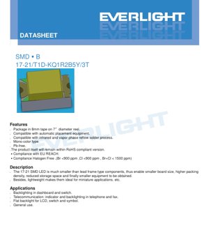
The 17-21/T1D-KQ1R2B5Y/3T is a compact, surface-mount device (SMD) LED designed for modern electronic applications requiring miniaturization and high reliability. This mono-color LED emits a pure white light, achieved through an InGaN chip encapsulated in a yellow diffused resin. Its primary advantage lies in its significantly reduced footprint compared to traditional lead-frame LEDs, enabling higher component packing density on printed circuit boards (PCBs), reduced equipment storage space, and ultimately contributing to the development of smaller, lighter end-user devices. The component is fully RoHS compliant, adheres to EU REACH regulations, and is manufactured as a halogen-free product, with bromine and chlorine content strictly controlled below industry standards.
1.1 Core Advantages and Target Market
The design philosophy behind the 17-21 SMD LED centers on enabling miniaturization. Its small physical dimensions directly translate to smaller required board space, allowing designers to create more compact products. The lightweight nature of the package makes it particularly suitable for portable and miniature applications where every gram matters. The device is supplied on 8mm tape mounted on 7-inch diameter reels, ensuring compatibility with high-speed, automated pick-and-place assembly equipment, which is critical for mass production. Its compatibility with both infrared and vapor phase reflow soldering processes provides flexibility in manufacturing. The primary target markets include consumer electronics, automotive interiors (specifically dashboard and switch backlighting), telecommunications equipment for status indicators, and general backlighting for LCDs and control panels.
2. Technical Parameter Deep-Dive
This section provides a detailed, objective analysis of the key electrical, optical, and thermal parameters defined in the datasheet, explaining their significance for circuit design and reliability.
2.1 Absolute Maximum Ratings
The Absolute Maximum Ratings define the stress limits beyond which permanent damage to the LED may occur. These are not conditions for normal operation but rather thresholds that must never be exceeded.
- Reverse Voltage (VR): 5V - Applying a reverse bias voltage greater than 5V can cause immediate junction breakdown. The datasheet explicitly notes that the device is not designed for reverse operation; this rating is primarily for the IR (reverse current) test condition. In application, external circuit protection (like a diode in parallel) is often necessary if reverse voltage is a possibility.
- Forward Current (IF): 10mA - This is the maximum continuous DC current recommended for reliable long-term operation. Exceeding this current increases junction temperature, accelerates lumen depreciation, and significantly shortens the device's lifespan.
- Peak Forward Current (IFP): 100mA - The LED can withstand short current pulses (with a duty cycle of 1/10 at 1kHz) up to 100mA. This is relevant for pulsed operation or momentary surges but should not be used for calculating steady-state power dissipation.
- Power Dissipation (Pd): 40mW - This is the maximum power the package can dissipate as heat at an ambient temperature (Ta) of 25°C. The actual power dissipated is calculated as Forward Voltage (VF) * Forward Current (IF). Operating near or above this limit requires careful thermal management.
- Operating & Storage Temperature: The device is rated for operation from -40°C to +85°C and can be stored from -40°C to +90°C. This wide range makes it suitable for automotive and industrial environments.
- Soldering Temperature: Two profiles are specified: 260°C for 10 seconds for reflow soldering (typical for Pb-free processes), and 350°C for 3 seconds for hand soldering. Adherence to these limits is critical to prevent damage to the internal die bond or the plastic package.
2.2 Electro-Optical Characteristics
These parameters are measured under standard test conditions (Ta=25°C, IF=5mA) and define the LED's performance.
- Luminous Intensity (Iv): 72.0 - 180.0 mcd (Typical) - This is the amount of visible light emitted in a specific direction. The very wide range (72 to 180 mcd) indicates that the LEDs are sorted into different "bins" based on measured output, which is detailed in a later section. The test current of 5mA is below the maximum rating, providing a safety margin for measurement.
- Viewing Angle (2θ1/2): 150° (Typical) - This is the angle at which the luminous intensity is half of the intensity at 0° (on-axis). A 150° viewing angle is very wide, producing a diffuse, lambertian-like emission pattern suitable for area illumination and backlighting where even light distribution is desired, rather than a focused beam.
- Forward Voltage (VF): 2.7V - 3.1V (Max) - This is the voltage drop across the LED when driven at the test current of 5mA. The variation is due to semiconductor process tolerances and is also managed through binning. A current-limiting resistor must always be used in series with the LED to set the operating current, as the VF is not a fixed value.
- Reverse Current (IR): 50 μA (Max) - This is the leakage current when 5V reverse bias is applied. It is typically very small in a healthy device.
3. Binning System Explanation
To ensure consistency in mass production, LEDs are tested and sorted into performance groups or "bins." The 17-21/T1D-KQ1R2B5Y/3T uses a multi-parameter binning system, as indicated by the code "KQ1R2B5Y".
3.1 Luminous Intensity Binning
The luminous intensity is sorted into four distinct bins (Q1, Q2, R1, R2). When specifying or ordering, the "R2" in the part number indicates the selected bin.
- Bin Q1: 72.0 - 90.0 mcd
- Bin Q2: 90.0 - 112.0 mcd
- Bin R1: 112.0 - 140.0 mcd
- Bin R2: 140.0 - 180.0 mcd
This allows designers to choose a brightness level appropriate for their application, with higher bins typically used where maximum light output is critical.
3.2 Forward Voltage Binning
Forward voltage is binned in 0.1V steps from 2.7V to 3.1V. The "B5" in the part number corresponds to one of these bins. Matching VF bins in a design can help ensure uniform current sharing when multiple LEDs are connected in parallel.
- Bin 29: 2.7 - 2.8V
- Bin 30: 2.8 - 2.9V
- Bin 31: 2.9 - 3.0V
- Bin 32: 3.0 - 3.1V
3.3 Chromaticity Coordinate Binning
The color of the white light is defined by its chromaticity coordinates (x, y) on the CIE 1931 diagram. The datasheet defines four quadrangular bins (3, 4, 5, 6) on this chart. The "Y" in the part number likely references the yellow diffused resin and the associated color bin (e.g., bin 5). The specified tolerance is ±0.01 in both x and y coordinates, which is a standard tolerance for white LEDs and ensures a consistent perceived color within a batch.
4. Mechanical and Package Information
4.1 Package Dimensions
The 17-21 SMD LED has a compact rectangular package. Key dimensions (in mm) include a typical body size of approximately 1.6mm in length and 0.8mm in width, with a height of around 0.6mm. The exact dimensions, including pad placement and tolerances (±0.1mm unless otherwise noted), are provided in the detailed package drawing. The cathode is clearly marked, which is essential for correct orientation during assembly. The small size necessitates precise PCB pad design to ensure proper soldering and mechanical stability.
4.2 Packaging and Handling
The components are delivered in moisture-sensitive device (MSD) packaging. They are supplied on embossed carrier tape (8mm pitch) wound onto 7-inch reels, with 3000 pieces per reel. The packaging includes a desiccant and is sealed within an aluminum moisture-proof bag. The reel label contains critical information: Customer Part Number (CPN), Manufacturer Part Number (P/N), quantity (QTY), and the specific bin codes for Luminous Intensity (CAT), Chromaticity (HUE), and Forward Voltage (REF).
5. Soldering and Assembly Guidelines
Proper handling and soldering are crucial for the reliability of SMD components.
5.1 Storage and Moisture Sensitivity
The LED is moisture sensitive (MSL classification implied). The bag should not be opened until the components are ready for use. After opening, unused LEDs must be stored at ≤30°C and ≤60% RH and used within 168 hours (7 days). If this window is exceeded or the desiccant indicates saturation, a bake-out at 60±5°C for 24 hours is required before use to remove absorbed moisture and prevent "popcorning" during reflow soldering.
5.2 Soldering Process
Reflow Soldering: A Pb-free reflow profile with a peak temperature of 260°C for up to 10 seconds is specified. The component should not undergo more than two reflow cycles. Stress on the LED body during heating must be avoided.
Hand Soldering: If necessary, hand soldering can be performed with an iron tip temperature ≤350°C for ≤3 seconds per terminal, using a low-power iron (≤25W). A cooling interval of >2 seconds between terminals is recommended. The datasheet strongly cautions that hand soldering often leads to damage.
Repair: Repair after soldering is discouraged. If unavoidable, a specialized double-head soldering iron must be used to simultaneously heat both terminals, preventing thermal stress on the die. The impact on LED characteristics must be evaluated beforehand.
6. Application Suggestions and Design Considerations
6.1 Typical Application Scenarios
- Backlighting: Ideal for dashboard instrument clusters, membrane switches, keypads, and symbols due to its wide viewing angle and even light distribution.
- Status Indicators: Perfect for power, connectivity, or function status lights in telecommunication equipment (phones, faxes), consumer electronics, and industrial controls.
- LCD Backlighting: Can be used for edge-lit or direct-lit backlighting in small monochrome or color LCD displays.
- General Purpose Indication: Any application requiring a compact, reliable, bright white indicator light.
6.2 Critical Design Considerations
- Current Limiting is Mandatory: An LED is a current-driven device. A series resistor must always be used to set the forward current. The datasheet warns that without it, a small change in supply voltage can cause a large, destructive change in current. The resistor value is calculated using Ohm's Law: R = (V_supply - VF_LED) / I_desired. Always use the maximum VF from the bin or datasheet for a conservative design.
- Thermal Management: While the package is small, power dissipation (up to 40mW) generates heat. For continuous operation at high currents (near 10mA), ensure the PCB has adequate thermal relief, especially if multiple LEDs are clustered. High junction temperatures reduce light output and lifespan.
- ESD Protection: The device has an ESD HBM rating of 150V, which is relatively low. Standard ESD precautions should be followed during handling and assembly.
- Optical Design: The 150° viewing angle and yellow diffused resin create a soft, wide beam. For focused illumination, external lenses or light guides would be required. The diffused resin helps in achieving uniform appearance when used behind a diffuser panel.
7. Technical Comparison and Differentiation
The 17-21 package sits in a category of very small SMD LEDs. Its key differentiators are its combination of a relatively high luminous intensity (up to 180 mcd) within an extremely small footprint (1.6x0.8mm). Compared to larger SMD LEDs (e.g., 3528, 5050), it offers superior space savings but may have lower total light output or power handling. Compared to even smaller chip LEDs, it offers easier handling due to its packaged form and integrated lens. The explicit binning for intensity, voltage, and chromaticity provides a level of performance consistency that is critical for applications requiring uniform appearance, such as backlighting arrays.
8. Frequently Asked Questions (Based on Technical Parameters)
Q: Why is the forward current limited to 10mA if it can handle 100mA pulses?
A: The 10mA rating is for continuous operation, ensuring long-term reliability and maintaining specified optical performance. The 100mA pulse rating is for short durations (e.g., 0.1ms every 1ms). Continuous operation at high current increases junction temperature, causing accelerated degradation of the phosphor and semiconductor, leading to premature dimming or failure.
Q: How do I choose the right current-limiting resistor?
A: Use the formula R = (V_supply - VF) / IF. For a 5V supply and a target current of 5mA, using the maximum VF of 3.1V for safety: R = (5 - 3.1) / 0.005 = 380 Ohms. The nearest standard value (390 Ohms) would be a good choice. Always verify power rating of the resistor: P = I^2 * R.
Q: Can I drive this LED directly from a microcontroller GPIO pin?
A: Possibly, but with caution. A typical GPIO pin can source/sink 20-25mA. You must include a series resistor. Also, ensure the microcontroller's output voltage is high enough to overcome the LED's VF (2.7-3.1V). A 3.3V microcontroller may work at the lower end of the VF range, but a 5V supply is more reliable. Never connect the LED directly between the pin and ground without a resistor.
Q: What does "Pb-free" and "Halogen-Free" mean for my application?
A: "Pb-free" means the solderable finishes do not contain lead, complying with environmental regulations like RoHS. "Halogen-Free" (Br <900ppm, Cl <900ppm, Br+Cl <1500ppm) means the plastic packaging material contains minimal halogens, which reduces the emission of toxic fumes if the device is exposed to extreme heat or fire, improving environmental and safety profiles.
9. Practical Design and Usage Case
Scenario: Designing a backlit keypad for a medical device.
The design requires 12 white indicator lights behind silicone rubber keys. Space is extremely limited on the double-sided PCB. The 17-21 LED is selected for its minimal footprint. The designer chooses the R2 luminous intensity bin to ensure good visibility in a brightly lit environment. All LEDs are specified from the same VF bin (e.g., 30) to promote even brightness when connected in a parallel configuration driven by a single current-limiting resistor per parallel branch (not a single resistor for all 12). The PCB layout places the thermal relief pads as per the datasheet drawing. The assembly house is instructed to follow the specified reflow profile and to keep the components in their sealed bag until the moment before placement. After assembly, the wide 150° viewing angle ensures each key is evenly illuminated without hot spots.
10. Operating Principle and Technology Trends
10.1 Basic Operating Principle
This is a phosphor-converted white LED. The core is a semiconductor chip made of Indium Gallium Nitride (InGaN) that emits light in the blue or near-ultraviolet spectrum when forward biased (electroluminescence). This primary light is then absorbed by a phosphor layer—a yellow-emitting phosphor in this case, suspended in the diffused resin encapsulant. The phosphor re-emits light at longer wavelengths (yellow). The combination of the unconverted blue light from the chip and the converted yellow light from the phosphor results in the perception of "white" light. The exact shade (cool white, pure white, warm white) is determined by the composition and amount of phosphor used, which is controlled during manufacturing to hit the specified chromaticity bins.
10.2 Objective Technology Trends
The general trend in SMD LED technology continues toward several key objectives: Increased Efficiency (lm/W): Improving the light output per unit of electrical power input, reducing energy consumption and thermal load. Higher Reliability and Lifetime: Enhancing materials and packaging to withstand higher temperatures and more operating hours with minimal lumen depreciation. Improved Color Consistency and Rendering: Tighter binning tolerances and the development of phosphors that offer higher Color Rendering Index (CRI) values for more natural-looking white light. Further Miniaturization: The development of even smaller package footprints while maintaining or increasing light output. Integrated Solutions: The growth of LEDs with built-in current regulators, controllers, or multiple chips in a single package to simplify circuit design. The 17-21 LED represents a mature, cost-effective point in this ongoing evolution, optimized for reliable performance in space-constrained, high-volume applications.
LED Specification Terminology
Complete explanation of LED technical terms
Photoelectric Performance
| Term | Unit/Representation | Simple Explanation | Why Important |
|---|---|---|---|
| Luminous Efficacy | lm/W (lumens per watt) | Light output per watt of electricity, higher means more energy efficient. | Directly determines energy efficiency grade and electricity cost. |
| Luminous Flux | lm (lumens) | Total light emitted by source, commonly called "brightness". | Determines if the light is bright enough. |
| Viewing Angle | ° (degrees), e.g., 120° | Angle where light intensity drops to half, determines beam width. | Affects illumination range and uniformity. |
| CCT (Color Temperature) | K (Kelvin), e.g., 2700K/6500K | Warmth/coolness of light, lower values yellowish/warm, higher whitish/cool. | Determines lighting atmosphere and suitable scenarios. |
| CRI / Ra | Unitless, 0–100 | Ability to render object colors accurately, Ra≥80 is good. | Affects color authenticity, used in high-demand places like malls, museums. |
| SDCM | MacAdam ellipse steps, e.g., "5-step" | Color consistency metric, smaller steps mean more consistent color. | Ensures uniform color across same batch of LEDs. |
| Dominant Wavelength | nm (nanometers), e.g., 620nm (red) | Wavelength corresponding to color of colored LEDs. | Determines hue of red, yellow, green monochrome LEDs. |
| Spectral Distribution | Wavelength vs intensity curve | Shows intensity distribution across wavelengths. | Affects color rendering and quality. |
Electrical Parameters
| Term | Symbol | Simple Explanation | Design Considerations |
|---|---|---|---|
| Forward Voltage | Vf | Minimum voltage to turn on LED, like "starting threshold". | Driver voltage must be ≥Vf, voltages add up for series LEDs. |
| Forward Current | If | Current value for normal LED operation. | Usually constant current drive, current determines brightness & lifespan. |
| Max Pulse Current | Ifp | Peak current tolerable for short periods, used for dimming or flashing. | Pulse width & duty cycle must be strictly controlled to avoid damage. |
| Reverse Voltage | Vr | Max reverse voltage LED can withstand, beyond may cause breakdown. | Circuit must prevent reverse connection or voltage spikes. |
| Thermal Resistance | Rth (°C/W) | Resistance to heat transfer from chip to solder, lower is better. | High thermal resistance requires stronger heat dissipation. |
| ESD Immunity | V (HBM), e.g., 1000V | Ability to withstand electrostatic discharge, higher means less vulnerable. | Anti-static measures needed in production, especially for sensitive LEDs. |
Thermal Management & Reliability
| Term | Key Metric | Simple Explanation | Impact |
|---|---|---|---|
| Junction Temperature | Tj (°C) | Actual operating temperature inside LED chip. | Every 10°C reduction may double lifespan; too high causes light decay, color shift. |
| Lumen Depreciation | L70 / L80 (hours) | Time for brightness to drop to 70% or 80% of initial. | Directly defines LED "service life". |
| Lumen Maintenance | % (e.g., 70%) | Percentage of brightness retained after time. | Indicates brightness retention over long-term use. |
| Color Shift | Δu′v′ or MacAdam ellipse | Degree of color change during use. | Affects color consistency in lighting scenes. |
| Thermal Aging | Material degradation | Deterioration due to long-term high temperature. | May cause brightness drop, color change, or open-circuit failure. |
Packaging & Materials
| Term | Common Types | Simple Explanation | Features & Applications |
|---|---|---|---|
| Package Type | EMC, PPA, Ceramic | Housing material protecting chip, providing optical/thermal interface. | EMC: good heat resistance, low cost; Ceramic: better heat dissipation, longer life. |
| Chip Structure | Front, Flip Chip | Chip electrode arrangement. | Flip chip: better heat dissipation, higher efficacy, for high-power. |
| Phosphor Coating | YAG, Silicate, Nitride | Covers blue chip, converts some to yellow/red, mixes to white. | Different phosphors affect efficacy, CCT, and CRI. |
| Lens/Optics | Flat, Microlens, TIR | Optical structure on surface controlling light distribution. | Determines viewing angle and light distribution curve. |
Quality Control & Binning
| Term | Binning Content | Simple Explanation | Purpose |
|---|---|---|---|
| Luminous Flux Bin | Code e.g., 2G, 2H | Grouped by brightness, each group has min/max lumen values. | Ensures uniform brightness in same batch. |
| Voltage Bin | Code e.g., 6W, 6X | Grouped by forward voltage range. | Facilitates driver matching, improves system efficiency. |
| Color Bin | 5-step MacAdam ellipse | Grouped by color coordinates, ensuring tight range. | Guarantees color consistency, avoids uneven color within fixture. |
| CCT Bin | 2700K, 3000K etc. | Grouped by CCT, each has corresponding coordinate range. | Meets different scene CCT requirements. |
Testing & Certification
| Term | Standard/Test | Simple Explanation | Significance |
|---|---|---|---|
| LM-80 | Lumen maintenance test | Long-term lighting at constant temperature, recording brightness decay. | Used to estimate LED life (with TM-21). |
| TM-21 | Life estimation standard | Estimates life under actual conditions based on LM-80 data. | Provides scientific life prediction. |
| IESNA | Illuminating Engineering Society | Covers optical, electrical, thermal test methods. | Industry-recognized test basis. |
| RoHS / REACH | Environmental certification | Ensures no harmful substances (lead, mercury). | Market access requirement internationally. |
| ENERGY STAR / DLC | Energy efficiency certification | Energy efficiency and performance certification for lighting. | Used in government procurement, subsidy programs, enhances competitiveness. |