Table of Contents
- 1. Product Overview
- 1.1 Core Advantages and Target Market
- 2. In-Depth Technical Parameter Analysis
- 2.1 Absolute Maximum Ratings
- 2.2 Electro-Optical Characteristics
- 3. Binning System Explanation
- 4. Performance Curve Analysis
- 5. Mechanical and Package Information
- 5.1 Package Dimensions
- 5.2 Polarity Identification
- 6. Soldering and Assembly Guidelines
- 6.1 Storage and Moisture Sensitivity
- 6.2 Reflow Soldering Profile
- 6.3 Hand Soldering and Rework
- 7. Packaging and Ordering Information
- 7.1 Packaging Specification
- 7.2 Label Explanation
- 8. Application Design Suggestions
- 8.1 Typical Application Circuits
- 8.2 Design Considerations
- 9. Technical Comparison and Differentiation
- 10. Frequently Asked Questions (FAQ)
- 11. Practical Design and Usage Case
- 12. Operating Principle Introduction
- 13. Technology Trends and Developments
1. Product Overview
The 19-217 is a surface-mount device (SMD) LED designed for general-purpose indicator and backlighting applications. It utilizes an AlGaInP chip to produce a brilliant red light output. Its compact SMD package enables significant advantages in modern electronic design, including reduced board space, higher component packing density, and overall miniaturization of end equipment. The device is compliant with key environmental and safety standards, including RoHS, REACH, and halogen-free requirements.
1.1 Core Advantages and Target Market
The primary advantages of this LED stem from its miniature SMD form factor. Compared to traditional lead-frame LEDs, it allows for smaller printed circuit board (PCB) designs, reduced storage space requirements, and lighter final products. This makes it particularly suitable for applications where space and weight are critical constraints. The device is targeted at a broad range of markets including consumer electronics, telecommunications equipment (e.g., phones, fax machines), automotive dashboard and switch backlighting, and general indicator applications where a reliable, compact red light source is needed.
2. In-Depth Technical Parameter Analysis
This section provides a detailed, objective interpretation of the key electrical, optical, and thermal parameters defined in the datasheet. Understanding these limits and typical values is crucial for reliable circuit design.
2.1 Absolute Maximum Ratings
The Absolute Maximum Ratings define the stress limits beyond which permanent damage to the device may occur. These are not operating conditions.
- Reverse Voltage (VR): 5V - Applying a reverse bias voltage exceeding 5V can cause junction breakdown.
- Forward Current (IF): 25mA - The maximum continuous DC current that can be passed through the LED.
- Peak Forward Current (IFP): 60mA - A pulsed current limit (1/10 duty cycle, 1kHz) for brief, high-intensity flashes. Exceeding the continuous current rating without proper pulsing will lead to overheating.
- Power Dissipation (Pd): 60mW - The maximum power the package can dissipate as heat, calculated as Forward Voltage (VF) * Forward Current (IF).
- ESD (HBM): 2000V - The LED has a Human Body Model electrostatic discharge rating of 2kV. Proper ESD handling precautions are necessary during assembly.
- Operating & Storage Temperature: -40°C to +85°C / -40°C to +90°C - Specifies the full environmental range for use and non-operating storage.
- Soldering Temperature: The device can withstand reflow soldering with a peak temperature of 260°C for up to 10 seconds, or hand soldering at 350°C for up to 3 seconds per terminal.
2.2 Electro-Optical Characteristics
These parameters are measured at a standard test condition of Ta=25°C and IF=20mA, unless otherwise specified. They define the typical performance of the LED.
- Luminous Intensity (Iv): 45.0 - 112 mcd (Typ. not specified) - The amount of visible light emitted. The wide range indicates a binning system is used (see Section 3). The test current is 20mA.
- Viewing Angle (2θ1/2): 120° (Typical) - The angle at which the luminous intensity is half of the intensity at 0° (on-axis). This is a very wide viewing angle, suitable for applications requiring broad visibility.
- Peak Wavelength (λp): 632 nm (Typical) - The wavelength at which the optical output power is maximum. For AlGaInP red LEDs, this typically falls in the orange-red to red region.
- Dominant Wavelength (λd): 624 nm (Typical) - The single wavelength perceived by the human eye that matches the color of the LED light. It is often slightly shorter than the peak wavelength for red LEDs.
- Spectral Bandwidth (Δλ): 20 nm (Typical) - The width of the emitted spectrum at half the maximum power (FWHM). A value of 20nm indicates a relatively pure color.
- Forward Voltage (VF): 1.7V - 2.4V (Typ. 2.0V) - The voltage drop across the LED when driven at 20mA. Designers must use this to calculate the required current-limiting resistor value. The typical value of 2.0V is a key design parameter.
- Reverse Current (IR): 10 μA Max. - The small leakage current that flows when the specified reverse voltage (5V) is applied.
3. Binning System Explanation
The datasheet outlines a luminous intensity binning system to ensure consistency in brightness for production applications. The specific device code "P1Q2" in the part number refers to its bin.
- Bin Code P1: Luminous Intensity from 45.0 mcd to 57.0 mcd.
- Bin Code P2: Luminous Intensity from 57.0 mcd to 72.0 mcd.
- Bin Code Q1: Luminous Intensity from 72.0 mcd to 90.0 mcd.
- Bin Code Q2: Luminous Intensity from 90.0 mcd to 112 mcd.
The part number suffix "P1Q2/3T" indicates this specific device falls into the Q2 bin for luminous intensity. Designers can select the appropriate bin based on the required brightness level for their application. The datasheet also notes a general tolerance of ±11% on luminous intensity within a bin.
4. Performance Curve Analysis
While the PDF references "Typical Electro-Optical Characteristics Curves," the specific graphs are not provided in the text. Based on standard LED behavior, these curves would typically include:
- IV Curve (Current vs. Voltage): Shows the exponential relationship between forward voltage and forward current. The "knee" voltage is around the typical VF of 2.0V. This curve is essential for designing the driver circuit.
- Luminous Intensity vs. Forward Current: Demonstrates how light output increases with current, typically in a near-linear relationship within the operating range, before efficiency drops at very high currents due to heating.
- Luminous Intensity vs. Ambient Temperature: Shows the derating of light output as the junction temperature increases. For most LEDs, output decreases as temperature rises.
- Spectral Distribution: A plot of relative intensity versus wavelength, showing the peak at ~632nm and the ~20nm bandwidth.
Designers should consult the full graphical datasheet from the manufacturer for these detailed curves to optimize performance over temperature and drive conditions.
5. Mechanical and Package Information
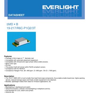
5.1 Package Dimensions
The LED is housed in a standard SMD package. The drawing in the datasheet provides critical dimensions including body length, width, height, and the placement of the cathode/anode terminals. The cathode is typically identified by a visual marker such as a notch, green dot, or truncated corner on the package. The dimensional tolerance is generally ±0.1mm unless otherwise noted. Precise footprint layout is necessary for successful automated pick-and-place and soldering.
5.2 Polarity Identification
Correct polarity is essential for LED operation. The datasheet's package diagram will clearly indicate the cathode (negative) terminal. Mounting the LED in reverse bias will prevent it from lighting and, if the reverse voltage rating is exceeded, may damage the device.
6. Soldering and Assembly Guidelines
Proper handling is critical to maintain reliability. The datasheet provides detailed instructions.
6.1 Storage and Moisture Sensitivity
The LEDs are packaged in a moisture-resistant bag with desiccant. The bag should not be opened until the components are ready for use. If the bag is opened and components are not used immediately, they have a "floor life" of 1 year under controlled conditions (≤30°C, ≤60% RH). Exceeding this or if the desiccant indicator changes color, a baking treatment (60±5°C for 24 hours) is required before reflow soldering to prevent "popcorning" damage from moisture vaporization.
6.2 Reflow Soldering Profile
A lead-free reflow profile is specified:
- Pre-heating: 150-200°C for 60-120 seconds.
- Time Above Liquidus (217°C): 60-150 seconds.
- Peak Temperature: 260°C maximum, held for no more than 10 seconds.
- Ramp-up Rate: Maximum 6°C/second.
- Ramp-down Rate: Maximum 3°C/second.
6.3 Hand Soldering and Rework
If hand soldering is necessary, the iron tip temperature must be below 350°C, applied for no more than 3 seconds per terminal. A low-power iron (≤25W) is recommended. A cooling interval of at least 2 seconds should be allowed between soldering each terminal. Rework is strongly discouraged, but if unavoidable, a specialized double-head soldering iron should be used to simultaneously heat both terminals and avoid mechanical stress on the solder joints.
7. Packaging and Ordering Information
7.1 Packaging Specification
The LEDs are supplied in industry-standard 8mm wide embossed carrier tape, wound onto a 7-inch diameter reel. Each reel contains 3000 pieces. The reel, tape, and cover tape dimensions are provided in the datasheet to ensure compatibility with automated assembly equipment.
7.2 Label Explanation
The reel label contains several key fields:
- P/N: Product Number (e.g., 19-217/R6C-P1Q2/3T).
- QTY: Packing Quantity (3000 pcs).
- CAT: Luminous Intensity Rank (e.g., Q2).
- HUE: Chromaticity Coordinates & Dominant Wavelength Rank.
- REF: Forward Voltage Rank.
- LOT No: Manufacturing Lot Number for traceability.
8. Application Design Suggestions
8.1 Typical Application Circuits
The most common drive method is a simple series resistor. The resistor value (R) is calculated using Ohm's Law: R = (Vsupply - VF) / IF. For example, with a 5V supply, a typical VF of 2.0V, and a desired IF of 20mA: R = (5V - 2.0V) / 0.020A = 150 Ω. The resistor power rating should be at least (Vsupply - VF) * IF = 0.06W; a 1/8W or 1/10W resistor is sufficient. This resistor is mandatory to prevent over-current, as the LED's exponential IV characteristic means a small voltage increase causes a large current surge that can instantly destroy the device.
8.2 Design Considerations
- Current Drive: Always drive with a constant current or a voltage source with a series resistor. Never connect directly to a voltage source.
- Thermal Management: While the package is small, ensuring adequate PCB copper area around the thermal pads (if any) or general board ventilation helps maintain lower junction temperature, preserving light output and longevity.
- ESD Protection: Implement ESD protection on input lines if the LED is in a user-accessible location, and follow ESD-safe handling procedures during assembly.
9. Technical Comparison and Differentiation
The 19-217's primary differentiation lies in its combination of a very wide 120-degree viewing angle and its specific brilliant red color point (λd ~624nm) from the AlGaInP material system. Compared to older technologies or narrower-angle LEDs, it provides more uniform off-axis visibility, which is advantageous for panel indicators and backlighting where the viewer may not be directly in front of the device. Its compliance with modern environmental standards (RoHS, Halogen-Free) is also a key requirement for most contemporary electronics manufacturing.
10. Frequently Asked Questions (FAQ)
Q: Can I drive this LED at 30mA for more brightness?
A: No. The Absolute Maximum Rating for continuous forward current is 25mA. Exceeding this rating risks overheating and premature failure. For higher brightness, select an LED from a higher luminous intensity bin (e.g., Q2) or a different product rated for higher current.
Q: The datasheet shows a typical VF of 2.0V, but my circuit measures 2.2V. Is this normal?
A: Yes. The Forward Voltage has a specified range from 1.7V to 2.4V. A value of 2.2V is well within the maximum limit and is normal due to manufacturing variations. Your current-limiting resistor calculation should use the maximum VF (2.4V) to guarantee the current never exceeds 25mA under worst-case conditions.
Q: Do I need to bake the LEDs if the bag has been opened for a week?
A: It depends on the storage environment. If they were stored in a controlled environment meeting the floor life conditions (≤30°C, ≤60% RH), baking may not be necessary. However, if the storage conditions are unknown or humid, performing the recommended bake (60°C for 24 hours) is a safe practice to prevent soldering defects.
11. Practical Design and Usage Case
Scenario: Designing a status indicator panel with multiple red LEDs.
A designer is creating a control panel that requires 10 uniform red status indicators. They select the 19-217/Q2 bin LED for consistent brightness. The panel is powered by a 3.3V rail. Using the maximum VF of 2.4V to ensure safe operation under all conditions, they calculate the series resistor: R = (3.3V - 2.4V) / 0.020A = 45 Ω. The nearest standard value is 47 Ω. The actual current with a typical VF of 2.0V would be ~27.7mA, which is slightly above the absolute maximum. Therefore, to stay within the 25mA limit under all conditions, they should use a larger resistor. Recalculating with a target of 20mA at max VF: R = (3.3V - 2.4V) / 0.020A = 45 Ω. At typical VF (2.0V), the current would be (3.3V-2.0V)/47Ω = 27.7mA, which is too high. A better approach is to design for the typical case but verify the max current: Choose R = (3.3V - 2.0V) / 0.020A = 65 Ω (use 68 Ω). Max current at VF_min (1.7V) = (3.3V-1.7V)/68Ω = 23.5mA (safe). This case highlights the importance of considering the full VF range in resistor calculation.
12. Operating Principle Introduction
Light Emitting Diodes (LEDs) are semiconductor devices that emit light through electroluminescence. When a forward voltage is applied across the p-n junction, electrons from the n-type region and holes from the p-type region are injected into the active region. When these charge carriers (electrons and holes) recombine, they release energy. In an AlGaInP (Aluminum Gallium Indium Phosphide) LED like the 19-217, this energy is released primarily as photons (light) in the red portion of the visible spectrum. The specific wavelengths (peak at 632nm, dominant at 624nm) are determined by the precise bandgap energy of the semiconductor material, which is engineered during the crystal growth process. The wide 120-degree viewing angle is achieved through the shape and material of the epoxy lens that encapsulates the semiconductor chip.
13. Technology Trends and Developments
The trend in SMD indicator LEDs continues towards higher efficiency, smaller package sizes, and improved reliability. While the 19-217 uses a proven AlGaInP technology for red, newer materials and chip designs can offer higher luminous efficacy (more light output per electrical watt). There is also a growing emphasis on tighter binning tolerances for both color and intensity to meet the demands of applications requiring high uniformity, such as full-color displays and automotive lighting clusters. Furthermore, the drive for miniaturization persists, pushing packages smaller than the traditional 2.0mm x 1.25mm footprint. The environmental compliance standards (Halogen-Free, REACH) highlighted in this datasheet are now baseline requirements for virtually all electronic components sold globally.
LED Specification Terminology
Complete explanation of LED technical terms
Photoelectric Performance
| Term | Unit/Representation | Simple Explanation | Why Important |
|---|---|---|---|
| Luminous Efficacy | lm/W (lumens per watt) | Light output per watt of electricity, higher means more energy efficient. | Directly determines energy efficiency grade and electricity cost. |
| Luminous Flux | lm (lumens) | Total light emitted by source, commonly called "brightness". | Determines if the light is bright enough. |
| Viewing Angle | ° (degrees), e.g., 120° | Angle where light intensity drops to half, determines beam width. | Affects illumination range and uniformity. |
| CCT (Color Temperature) | K (Kelvin), e.g., 2700K/6500K | Warmth/coolness of light, lower values yellowish/warm, higher whitish/cool. | Determines lighting atmosphere and suitable scenarios. |
| CRI / Ra | Unitless, 0–100 | Ability to render object colors accurately, Ra≥80 is good. | Affects color authenticity, used in high-demand places like malls, museums. |
| SDCM | MacAdam ellipse steps, e.g., "5-step" | Color consistency metric, smaller steps mean more consistent color. | Ensures uniform color across same batch of LEDs. |
| Dominant Wavelength | nm (nanometers), e.g., 620nm (red) | Wavelength corresponding to color of colored LEDs. | Determines hue of red, yellow, green monochrome LEDs. |
| Spectral Distribution | Wavelength vs intensity curve | Shows intensity distribution across wavelengths. | Affects color rendering and quality. |
Electrical Parameters
| Term | Symbol | Simple Explanation | Design Considerations |
|---|---|---|---|
| Forward Voltage | Vf | Minimum voltage to turn on LED, like "starting threshold". | Driver voltage must be ≥Vf, voltages add up for series LEDs. |
| Forward Current | If | Current value for normal LED operation. | Usually constant current drive, current determines brightness & lifespan. |
| Max Pulse Current | Ifp | Peak current tolerable for short periods, used for dimming or flashing. | Pulse width & duty cycle must be strictly controlled to avoid damage. |
| Reverse Voltage | Vr | Max reverse voltage LED can withstand, beyond may cause breakdown. | Circuit must prevent reverse connection or voltage spikes. |
| Thermal Resistance | Rth (°C/W) | Resistance to heat transfer from chip to solder, lower is better. | High thermal resistance requires stronger heat dissipation. |
| ESD Immunity | V (HBM), e.g., 1000V | Ability to withstand electrostatic discharge, higher means less vulnerable. | Anti-static measures needed in production, especially for sensitive LEDs. |
Thermal Management & Reliability
| Term | Key Metric | Simple Explanation | Impact |
|---|---|---|---|
| Junction Temperature | Tj (°C) | Actual operating temperature inside LED chip. | Every 10°C reduction may double lifespan; too high causes light decay, color shift. |
| Lumen Depreciation | L70 / L80 (hours) | Time for brightness to drop to 70% or 80% of initial. | Directly defines LED "service life". |
| Lumen Maintenance | % (e.g., 70%) | Percentage of brightness retained after time. | Indicates brightness retention over long-term use. |
| Color Shift | Δu′v′ or MacAdam ellipse | Degree of color change during use. | Affects color consistency in lighting scenes. |
| Thermal Aging | Material degradation | Deterioration due to long-term high temperature. | May cause brightness drop, color change, or open-circuit failure. |
Packaging & Materials
| Term | Common Types | Simple Explanation | Features & Applications |
|---|---|---|---|
| Package Type | EMC, PPA, Ceramic | Housing material protecting chip, providing optical/thermal interface. | EMC: good heat resistance, low cost; Ceramic: better heat dissipation, longer life. |
| Chip Structure | Front, Flip Chip | Chip electrode arrangement. | Flip chip: better heat dissipation, higher efficacy, for high-power. |
| Phosphor Coating | YAG, Silicate, Nitride | Covers blue chip, converts some to yellow/red, mixes to white. | Different phosphors affect efficacy, CCT, and CRI. |
| Lens/Optics | Flat, Microlens, TIR | Optical structure on surface controlling light distribution. | Determines viewing angle and light distribution curve. |
Quality Control & Binning
| Term | Binning Content | Simple Explanation | Purpose |
|---|---|---|---|
| Luminous Flux Bin | Code e.g., 2G, 2H | Grouped by brightness, each group has min/max lumen values. | Ensures uniform brightness in same batch. |
| Voltage Bin | Code e.g., 6W, 6X | Grouped by forward voltage range. | Facilitates driver matching, improves system efficiency. |
| Color Bin | 5-step MacAdam ellipse | Grouped by color coordinates, ensuring tight range. | Guarantees color consistency, avoids uneven color within fixture. |
| CCT Bin | 2700K, 3000K etc. | Grouped by CCT, each has corresponding coordinate range. | Meets different scene CCT requirements. |
Testing & Certification
| Term | Standard/Test | Simple Explanation | Significance |
|---|---|---|---|
| LM-80 | Lumen maintenance test | Long-term lighting at constant temperature, recording brightness decay. | Used to estimate LED life (with TM-21). |
| TM-21 | Life estimation standard | Estimates life under actual conditions based on LM-80 data. | Provides scientific life prediction. |
| IESNA | Illuminating Engineering Society | Covers optical, electrical, thermal test methods. | Industry-recognized test basis. |
| RoHS / REACH | Environmental certification | Ensures no harmful substances (lead, mercury). | Market access requirement internationally. |
| ENERGY STAR / DLC | Energy efficiency certification | Energy efficiency and performance certification for lighting. | Used in government procurement, subsidy programs, enhances competitiveness. |