Table of Contents
- 1. Product Overview
- 2. Technical Parameter Deep Dive
- 2.1 Absolute Maximum Ratings
- 2.2 Electro-Optical Characteristics
- 3. Binning System Explanation
- 3.1 Luminous Intensity Binning
- 3.2 Dominant Wavelength Binning
- 3.3 Forward Voltage Binning
- 4. Performance Curve Analysis
- 5. Mechanical and Package Information
- 6. Soldering and Assembly Guidelines
- 7. Packaging and Ordering Information
- 8. Application Suggestions
- 8.1 Typical Application Scenarios
- 8.2 Design Considerations
- 9. Technical Comparison & Differentiation
- 10. Frequently Asked Questions (Based on Technical Parameters)
- 11. Practical Design and Usage Case
- 12. Principle Introduction
- 13. Development Trends
1. Product Overview
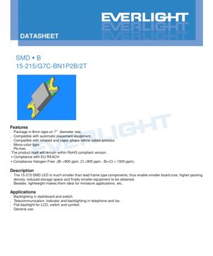
The 15-215/G7C-BN1P2B/2T is a surface-mount device (SMD) LED utilizing an AlGaInP (Aluminum Gallium Indium Phosphide) semiconductor chip to emit a Brilliant Yellow Green light. This LED is characterized by its compact size, which facilitates smaller printed circuit board (PCB) designs, higher component packing density, and ultimately enables the development of more miniature electronic equipment. Its lightweight construction further enhances its suitability for applications where space and weight are critical constraints.
The device is packaged on 8mm tape wound onto a 7-inch diameter reel, making it fully compatible with standard automated pick-and-place assembly equipment. It is designed for use with both infrared and vapor phase reflow soldering processes. The product is compliant with key environmental and safety regulations, being lead-free (Pb-free), compliant with the EU RoHS directive, EU REACH regulations, and meeting halogen-free standards (Bromine <900 ppm, Chlorine <900 ppm, Br+Cl < 1500 ppm).
2. Technical Parameter Deep Dive
2.1 Absolute Maximum Ratings
The absolute maximum ratings define the limits beyond which permanent damage to the device may occur. These ratings are specified at an ambient temperature (Ta) of 25°C. The maximum reverse voltage (VR) is 5V. The maximum continuous forward current (IF) is 25 mA. For pulsed operation, a peak forward current (IFP) of 60 mA is permissible under a duty cycle of 1/10 at 1 kHz. The maximum power dissipation (Pd) is 60 mW. The device can withstand an electrostatic discharge (ESD) of 2000V per the Human Body Model (HBM). The operational temperature range (Topr) is from -40°C to +85°C, while the storage temperature range (Tstg) is from -40°C to +90°C. For soldering, it can endure reflow soldering at 260°C for 10 seconds or hand soldering at 350°C for a maximum of 3 seconds.
2.2 Electro-Optical Characteristics
The core performance is defined under standard test conditions (Ta=25°C, IF=20mA). The luminous intensity (Iv) has a typical range. The device features a wide viewing angle (2θ1/2) of approximately 140 degrees. The peak wavelength (λp) is around 575 nm, with a dominant wavelength (λd) ranging from 567.5 nm to 575.5 nm. The spectral bandwidth (Δλ) is typically 20 nm. The forward voltage (VF) ranges from 1.75V to 2.35V. The reverse current (IR) is a maximum of 10 μA when a reverse voltage (VR) of 5V is applied. It is crucial to note that the device is not designed for operation under reverse bias; the VR rating is solely for testing the IR parameter.
3. Binning System Explanation
To ensure consistency in production, LEDs are sorted into bins based on key parameters. This allows designers to select parts that meet specific performance criteria for their application.
3.1 Luminous Intensity Binning
Luminous intensity is categorized into four bins (N1, N2, P1, P2) measured at IF=20mA. The bins define minimum and maximum values to guarantee a certain brightness level. Designers must account for an additional ±11% tolerance on the luminous intensity within a bin.
3.2 Dominant Wavelength Binning
The color, defined by dominant wavelength, is sorted into four bins (C15, C16, C17, C18), each covering a 2 nm range from 567.5 nm to 575.5 nm. A tolerance of ±1 nm applies to the dominant wavelength within a bin.
3.3 Forward Voltage Binning
Forward voltage is grouped into three bins (0, 1, 2), each spanning a 0.2V range from 1.75V to 2.35V. A tolerance of ±0.1V applies to the forward voltage within a bin. This binning is critical for designing consistent current-driving circuits, especially when multiple LEDs are connected in parallel.
4. Performance Curve Analysis
The datasheet provides several characteristic curves that illustrate device behavior under varying conditions. The Relative Luminous Intensity vs. Forward Current curve shows how light output increases with current, typically in a sub-linear fashion at higher currents due to heating and efficiency droop. The Forward Current Derating Curve is essential for thermal management; it indicates the maximum allowable forward current must be reduced as the ambient temperature increases above 25°C to prevent exceeding the maximum junction temperature and power dissipation limits. The Spectrum Distribution graph depicts the relative radiant power as a function of wavelength, centered around 575 nm with the characteristic 20 nm bandwidth. The Forward Current vs. Forward Voltage (I-V Curve) demonstrates the exponential relationship typical of a diode; a small increase in voltage leads to a large increase in current, underscoring the necessity for current-limiting circuitry. The Radiation Diagram (polar plot) visually represents the spatial distribution of light intensity, confirming the 140-degree viewing angle.
5. Mechanical and Package Information
The package drawing provides critical dimensions for PCB footprint design. Key measurements include the overall length and width, the size and position of the solder pads, and the component height. Tolerances are typically ±0.1mm unless otherwise specified. The polarity is indicated on the device itself, which must be correctly aligned with the corresponding polarity marking on the PCB footprint to ensure proper operation.
6. Soldering and Assembly Guidelines
Proper handling and soldering are vital for reliability. The device is supplied in moisture-sensitive packaging. The bag must not be opened until the components are ready for use. Once opened, LEDs should be stored at ≤30°C and ≤60% relative humidity and used within 168 hours (7 days). If this time is exceeded or the desiccant indicator shows saturation, a baking treatment at 60±5°C for 24 hours is required before use.
For Pb-free reflow soldering, a specific temperature profile must be followed: pre-heating between 150-200°C for 60-120 seconds, a time above liquidus (217°C) of 60-150 seconds, a peak temperature not exceeding 260°C held for a maximum of 10 seconds, and controlled cooling rates. Reflow soldering should not be performed more than twice. During hand soldering, the iron tip temperature must be below 350°C, contact time per terminal should not exceed 3 seconds, and a suitable interval should be left between soldering each terminal. Repair after initial soldering is discouraged, but if unavoidable, a specialized double-head soldering iron should be used to simultaneously heat both terminals and avoid mechanical stress.
7. Packaging and Ordering Information
The LEDs are delivered in a moisture-resistant packing system. They are loaded into carrier tape, which is then wound onto a 7-inch reel. Each reel contains 2000 pieces. The reel, along with desiccant, is sealed inside an aluminum moisture-proof bag. The bag label contains essential information for traceability and identification, including the product number, quantity, and the specific bin codes for luminous intensity (CAT), dominant wavelength (HUE), and forward voltage (REF).
8. Application Suggestions
8.1 Typical Application Scenarios
The Brilliant Yellow Green color and SMD format make this LED suitable for various indicator and backlighting roles. Primary applications include backlighting for instrument cluster dashboards and membrane switches, status indicators and keypad backlighting in telecommunication devices like phones and fax machines, and flat backlighting for small LCD panels, switches, and symbols. Its general-purpose nature also allows for use in consumer electronics, industrial controls, and portable devices.
8.2 Design Considerations
Current Drive: An external current-limiting resistor is mandatory. The exponential I-V characteristic means even a small variation in supply voltage can cause a large, potentially destructive, change in forward current. The resistor value must be calculated based on the supply voltage, the LED's forward voltage (considering the bin and tolerance), and the desired operating current (not exceeding 25 mA continuous).
Thermal Management: While the power dissipation is low, proper PCB layout is important. Ensure adequate copper area around the solder pads to act as a heat sink, especially if operating at high ambient temperatures or near the maximum current. Adhere to the current derating curve.
ESD Protection: Although rated for 2000V HBM, standard ESD precautions should be observed during handling and assembly.
9. Technical Comparison & Differentiation
Compared to traditional leaded LEDs, this SMD type offers significant advantages in size, weight, and suitability for automated assembly, leading to lower overall manufacturing costs. Within the SMD LED landscape, the use of AlGaInP material for yellow-green emission typically offers higher luminous efficiency and better color saturation than older technologies like GaP. The wide 140-degree viewing angle is a key feature for applications requiring broad visibility, as opposed to narrower-angle LEDs used for focused illumination. Its compliance with modern environmental standards (RoHS, Halogen-Free) is a baseline requirement for most contemporary electronic products.
10. Frequently Asked Questions (Based on Technical Parameters)
Q: What resistor value should I use with a 5V supply?
A: You must use the maximum forward voltage from the bin (e.g., 2.35V from Bin 2) and the desired current (e.g., 20mA). Using Ohm's Law: R = (Vsupply - Vf) / If = (5V - 2.35V) / 0.020A = 132.5 Ohms. A standard 130 or 150 Ohm resistor would be appropriate, ensuring the current does not exceed 25 mA even at the minimum Vf.
Q: Can I drive this LED without a current-limiting resistor using a constant voltage source?
A: No. This will almost certainly destroy the LED due to the uncontrolled current flow resulting from the diode's exponential I-V characteristic.
Q: How does temperature affect brightness?
A: Luminous intensity typically decreases as the junction temperature increases. The derating curve indirectly reflects this by requiring lower currents at high ambient temperatures to prevent overheating, which would further reduce efficiency and lifespan.
Q: What is the difference between peak wavelength and dominant wavelength?
A: Peak wavelength (λp) is the wavelength at which the spectral power distribution is maximum. Dominant wavelength (λd) is the single wavelength of monochromatic light that matches the perceived color of the LED. For a narrow-band emitter like this, they are often close, but λd is more relevant for color specification.
11. Practical Design and Usage Case
Case: Designing a multi-LED status indicator panel. A designer is creating a control panel with 10 yellow-green status indicators. To ensure uniform brightness, they should specify LEDs from the same luminous intensity bin (e.g., all P1). To ensure consistent color appearance, they should specify LEDs from the same dominant wavelength bin (e.g., all C17). To simplify the driver circuit and ensure even current distribution if LEDs are placed in parallel, specifying LEDs from the same forward voltage bin (e.g., all 1) is highly recommended. The driving circuit would consist of a voltage regulator (e.g., 5V) and a single current-limiting resistor for each LED (or a dedicated LED driver IC for better control and dimming capability). The PCB layout would group the LEDs together but provide sufficient copper pour for heat dissipation, especially if they are to be illuminated simultaneously for extended periods.
12. Principle Introduction
This LED operates on the principle of electroluminescence in a semiconductor p-n junction. When a forward voltage is applied, electrons from the n-type AlGaInP region are injected across the junction into the p-type region, and holes are injected in the opposite direction. These charge carriers recombine in the active region near the junction. In a direct bandgap semiconductor like AlGaInP, this recombination releases energy in the form of photons (light). The specific composition of the Aluminum, Gallium, Indium, and Phosphide atoms determines the bandgap energy, which directly dictates the wavelength (color) of the emitted light—in this case, Brilliant Yellow Green (~575 nm). The epoxy resin encapsulant serves to protect the semiconductor chip, shape the light output beam (creating the 140-degree viewing angle), and provide mechanical stability.
13. Development Trends
The general trend in SMD LEDs like this one continues towards higher luminous efficacy (more light output per electrical watt), improved color consistency and tighter binning tolerances, and enhanced reliability under harsh environmental conditions. Packaging is evolving to allow for even smaller footprints and lower profiles while maintaining or improving thermal performance. There is also a strong drive towards full-spectrum tunability and intelligent, addressable LEDs integrated with control circuitry. The underlying material science for AlGaInP LEDs is mature, but ongoing research focuses on optimizing efficiency at higher current densities and improving longevity. The emphasis on environmental compliance (halogen-free, RoHS) is now standard and will continue to be a baseline requirement for all electronic components.
LED Specification Terminology
Complete explanation of LED technical terms
Photoelectric Performance
| Term | Unit/Representation | Simple Explanation | Why Important |
|---|---|---|---|
| Luminous Efficacy | lm/W (lumens per watt) | Light output per watt of electricity, higher means more energy efficient. | Directly determines energy efficiency grade and electricity cost. |
| Luminous Flux | lm (lumens) | Total light emitted by source, commonly called "brightness". | Determines if the light is bright enough. |
| Viewing Angle | ° (degrees), e.g., 120° | Angle where light intensity drops to half, determines beam width. | Affects illumination range and uniformity. |
| CCT (Color Temperature) | K (Kelvin), e.g., 2700K/6500K | Warmth/coolness of light, lower values yellowish/warm, higher whitish/cool. | Determines lighting atmosphere and suitable scenarios. |
| CRI / Ra | Unitless, 0–100 | Ability to render object colors accurately, Ra≥80 is good. | Affects color authenticity, used in high-demand places like malls, museums. |
| SDCM | MacAdam ellipse steps, e.g., "5-step" | Color consistency metric, smaller steps mean more consistent color. | Ensures uniform color across same batch of LEDs. |
| Dominant Wavelength | nm (nanometers), e.g., 620nm (red) | Wavelength corresponding to color of colored LEDs. | Determines hue of red, yellow, green monochrome LEDs. |
| Spectral Distribution | Wavelength vs intensity curve | Shows intensity distribution across wavelengths. | Affects color rendering and quality. |
Electrical Parameters
| Term | Symbol | Simple Explanation | Design Considerations |
|---|---|---|---|
| Forward Voltage | Vf | Minimum voltage to turn on LED, like "starting threshold". | Driver voltage must be ≥Vf, voltages add up for series LEDs. |
| Forward Current | If | Current value for normal LED operation. | Usually constant current drive, current determines brightness & lifespan. |
| Max Pulse Current | Ifp | Peak current tolerable for short periods, used for dimming or flashing. | Pulse width & duty cycle must be strictly controlled to avoid damage. |
| Reverse Voltage | Vr | Max reverse voltage LED can withstand, beyond may cause breakdown. | Circuit must prevent reverse connection or voltage spikes. |
| Thermal Resistance | Rth (°C/W) | Resistance to heat transfer from chip to solder, lower is better. | High thermal resistance requires stronger heat dissipation. |
| ESD Immunity | V (HBM), e.g., 1000V | Ability to withstand electrostatic discharge, higher means less vulnerable. | Anti-static measures needed in production, especially for sensitive LEDs. |
Thermal Management & Reliability
| Term | Key Metric | Simple Explanation | Impact |
|---|---|---|---|
| Junction Temperature | Tj (°C) | Actual operating temperature inside LED chip. | Every 10°C reduction may double lifespan; too high causes light decay, color shift. |
| Lumen Depreciation | L70 / L80 (hours) | Time for brightness to drop to 70% or 80% of initial. | Directly defines LED "service life". |
| Lumen Maintenance | % (e.g., 70%) | Percentage of brightness retained after time. | Indicates brightness retention over long-term use. |
| Color Shift | Δu′v′ or MacAdam ellipse | Degree of color change during use. | Affects color consistency in lighting scenes. |
| Thermal Aging | Material degradation | Deterioration due to long-term high temperature. | May cause brightness drop, color change, or open-circuit failure. |
Packaging & Materials
| Term | Common Types | Simple Explanation | Features & Applications |
|---|---|---|---|
| Package Type | EMC, PPA, Ceramic | Housing material protecting chip, providing optical/thermal interface. | EMC: good heat resistance, low cost; Ceramic: better heat dissipation, longer life. |
| Chip Structure | Front, Flip Chip | Chip electrode arrangement. | Flip chip: better heat dissipation, higher efficacy, for high-power. |
| Phosphor Coating | YAG, Silicate, Nitride | Covers blue chip, converts some to yellow/red, mixes to white. | Different phosphors affect efficacy, CCT, and CRI. |
| Lens/Optics | Flat, Microlens, TIR | Optical structure on surface controlling light distribution. | Determines viewing angle and light distribution curve. |
Quality Control & Binning
| Term | Binning Content | Simple Explanation | Purpose |
|---|---|---|---|
| Luminous Flux Bin | Code e.g., 2G, 2H | Grouped by brightness, each group has min/max lumen values. | Ensures uniform brightness in same batch. |
| Voltage Bin | Code e.g., 6W, 6X | Grouped by forward voltage range. | Facilitates driver matching, improves system efficiency. |
| Color Bin | 5-step MacAdam ellipse | Grouped by color coordinates, ensuring tight range. | Guarantees color consistency, avoids uneven color within fixture. |
| CCT Bin | 2700K, 3000K etc. | Grouped by CCT, each has corresponding coordinate range. | Meets different scene CCT requirements. |
Testing & Certification
| Term | Standard/Test | Simple Explanation | Significance |
|---|---|---|---|
| LM-80 | Lumen maintenance test | Long-term lighting at constant temperature, recording brightness decay. | Used to estimate LED life (with TM-21). |
| TM-21 | Life estimation standard | Estimates life under actual conditions based on LM-80 data. | Provides scientific life prediction. |
| IESNA | Illuminating Engineering Society | Covers optical, electrical, thermal test methods. | Industry-recognized test basis. |
| RoHS / REACH | Environmental certification | Ensures no harmful substances (lead, mercury). | Market access requirement internationally. |
| ENERGY STAR / DLC | Energy efficiency certification | Energy efficiency and performance certification for lighting. | Used in government procurement, subsidy programs, enhances competitiveness. |