Table of Contents
- 1. Product Overview
- 1.1 Core Features and Compliance
- 1.2 Target Applications
- 2. Technical Parameters: In-Depth Objective Interpretation
- 2.1 Absolute Maximum Ratings
- 2.2 Electro-Optical Characteristics
- 3. Binning System Explanation
- 3.1 Luminous Intensity Binning
- 3.2 Forward Voltage Binning
- 3.3 Chromaticity Coordinate Binning
- 4. Performance Curve Analysis
- 5. Mechanical and Package Information
- 5.1 Package Dimensions
- 5.2 Polarity Identification and Pad Design
- 6. Soldering and Assembly Guidelines
- 6.1 Reflow Soldering Parameters
- 6.2 Storage and Moisture Sensitivity
- 6.3 Hand Soldering and Repair Precautions
- 7. Packaging and Ordering Information
- 7.1 Reel and Tape Specifications
- 7.2 Label Explanation
- 8. Application Suggestions and Design Considerations
- 8.1 Current Limiting and Protection
- 8.2 Thermal Management
- 8.3 ESD Protection
- 9. Technical Comparison and Differentiation
- 10. Frequently Asked Questions Based on Technical Parameters
- 10.1 What resistor value should I use with a 5V supply?
- 10.2 Can I drive this LED without a current-limiting resistor if I use a constant voltage source equal to Vf?
- 10.3 Why is the storage time after opening the bag limited to 7 days?
- 11. Practical Design and Usage Case
- 12. Operating Principle Introduction
- 13. Technology Trends
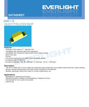
1. Product Overview
The 19-217/T7D-CT2V1N/3T is a compact, surface-mount LED designed for modern electronic applications requiring reliable indicator or backlighting functionality. This mono-color, Pure White LED utilizes an InGaN chip encapsulated in a yellow diffused resin. Its primary advantage lies in its significantly reduced footprint compared to traditional lead-frame components, enabling higher packing density on PCBs, reduced storage requirements, and ultimately contributing to the miniaturization of end equipment. The lightweight construction further makes it ideal for portable and space-constrained applications.
1.1 Core Features and Compliance
The device is supplied in 8mm tape on 7-inch diameter reels, ensuring compatibility with standard automated pick-and-place assembly equipment. It is designed for use with both infrared and vapor phase reflow soldering processes. The product adheres to several critical environmental and safety standards: it is Pb-free, compliant with the EU RoHS directive, meets EU REACH requirements, and is classified as Halogen-Free, with Bromine (Br) and Chlorine (Cl) content each below 900 ppm and their sum below 1500 ppm. This makes it suitable for use in markets with stringent environmental regulations.
1.2 Target Applications
The LED is versatile and finds use in multiple sectors. Common applications include backlighting for automotive dashboards and switches, indicator and backlighting functions in telecommunication devices such as telephones and fax machines, flat backlighting for LCDs, switches, and symbols, and general-purpose indicator use where a small, bright white light source is required.
2. Technical Parameters: In-Depth Objective Interpretation
This section provides a detailed breakdown of the electrical, optical, and thermal limits and characteristics of the LED, which are fundamental for reliable circuit design and system integration.
2.1 Absolute Maximum Ratings
The Absolute Maximum Ratings define the stress limits beyond which permanent damage to the device may occur. These values are not for continuous operation. The key ratings are: a maximum reverse voltage (VR) of 5V, a continuous forward current (IF) of 30mA, and a peak forward current (IFP) of 40mA permissible only under pulsed conditions (duty cycle 1/10 at 1kHz). The maximum power dissipation (Pd) is 110mW. The device can withstand an Electrostatic Discharge (ESD) of 150V per the Human Body Model (HBM). The operating temperature range (Topr) is from -40°C to +85°C, and the storage temperature (Tstg) ranges from -40°C to +90°C. Soldering temperature limits are specified for two processes: reflow soldering at 260°C for 10 seconds and hand soldering at 350°C for a maximum of 3 seconds.
2.2 Electro-Optical Characteristics
The Electro-Optical Characteristics are measured at a standard test condition of Ta=25°C and an IF of 20mA. The luminous intensity (Iv) has a typical range from 360.0 mcd to 900.0 mcd, with a tolerance of ±11%. The viewing angle (2θ1/2) is 130 degrees, providing a wide beam of light. The forward voltage (VF) ranges from 2.70V to 3.70V. The reverse current (IR) is specified at a maximum of 50 μA when a reverse voltage (VR) of 5V is applied. It is crucial to note that the device is not designed for operation in reverse bias; the VR rating is for IR testing purposes only.
3. Binning System Explanation
To ensure consistency in production, LEDs are sorted into performance bins. This system allows designers to select components that meet specific minimum performance criteria for their application.
3.1 Luminous Intensity Binning
The luminous output is categorized into four bin codes (T2, U1, U2, V1) based on minimum and maximum intensity values measured at IF=20mA. For example, bin code T2 covers intensities from 360.0 mcd to 450.0 mcd, while bin code V1 covers the highest range from 715.0 mcd to 900.0 mcd. Designers must account for the ±11% tolerance within each bin.
3.2 Forward Voltage Binning
The forward voltage is binned into five codes (10, 11, 12, 13, 14), each representing a 0.2V range. Code 10 spans 2.70V to 2.90V, and code 14 spans 3.50V to 3.70V. A tolerance of ±0.1V applies. Selecting LEDs from a specific voltage bin can help in designing more consistent current-limiting circuits, especially in parallel LED arrays.
3.3 Chromaticity Coordinate Binning
The color consistency of the Pure White light is controlled through chromaticity coordinate binning on the CIE 1931 diagram. The datasheet defines four bin codes (1, 2, 3, 4), each as a quadrilateral area on the (x, y) coordinate plane. For instance, Bin 1 is bounded by the points (0.274, 0.226), (0.274, 0.258), (0.294, 0.286), and (0.294, 0.254). The tolerance for these coordinates is ±0.01. This ensures the emitted white light falls within a predictable and narrow color range.
4. Performance Curve Analysis
While the PDF references typical electro-optical characteristic curves and a CIE Chromaticity Diagram on specific pages, the exact graphical data (e.g., IV curves, relative intensity vs. current, intensity vs. temperature) is not provided in the text content. In a complete datasheet, these curves are critical for understanding device behavior under non-standard conditions. Designers typically use such curves to extrapolate performance at different drive currents or ambient temperatures, to understand the spectral power distribution, and to visualize the color point on the chromaticity diagram relative to the defined bins and the Planckian locus.
5. Mechanical and Package Information
5.1 Package Dimensions
The LED has a compact SMD (Surface Mount Device) package. The dimensional drawing indicates key measurements including length, width, and height, with a standard tolerance of ±0.1mm unless otherwise noted. The specific dimensions define the footprint required on the PCB and the clearance needed above the board.
5.2 Polarity Identification and Pad Design
The package includes markings or structural features (like a chamfered corner or a dot) to indicate the cathode (negative) terminal, which is essential for correct orientation during assembly. The recommended land pattern (pad layout) on the PCB is typically provided to ensure proper soldering and mechanical stability.
6. Soldering and Assembly Guidelines
Proper handling and soldering are critical to maintaining LED performance and reliability.
6.1 Reflow Soldering Parameters
The device is rated for Pb-free reflow soldering with a peak temperature of 260°C for 10 seconds. A recommended temperature profile should be followed to gradually heat and cool the device, minimizing thermal shock. Reflow soldering should not be performed more than two times on the same device.
6.2 Storage and Moisture Sensitivity
The LEDs are packaged in moisture-resistant barrier bags with desiccant. The bag must not be opened until the components are ready for use. After opening, unused LEDs should be stored at ≤30°C and ≤60% Relative Humidity (RH) and used within 168 hours (7 days). If this window is exceeded or if the desiccant indicator shows saturation, a baking treatment at 60 ±5°C for 24 hours is required before use to remove absorbed moisture and prevent "popcorning" during reflow.
6.3 Hand Soldering and Repair Precautions
If hand soldering is necessary, the iron tip temperature must be below 350°C, and contact time per terminal should not exceed 3 seconds. A low-power iron (≤25W) is recommended. A cooling interval of at least 2 seconds should be observed between soldering each terminal. Repair after initial soldering is strongly discouraged. If unavoidable, a specialized double-head soldering iron should be used to simultaneously heat both terminals, preventing mechanical stress on the LED die. The potential for characteristic degradation due to repair must be evaluated beforehand.
7. Packaging and Ordering Information
7.1 Reel and Tape Specifications
The components are supplied on 7-inch diameter reels with 8mm wide carrier tape. Each reel contains 3000 pieces. Detailed reel dimensions and carrier tape pocket dimensions are provided to ensure compatibility with automated assembly equipment feeders.
7.2 Label Explanation
The packaging label contains several codes: CPN (Customer's Product Number), P/N (Product Number), QTY (Packing Quantity), CAT (Luminous Intensity Rank/Bin), HUE (Chromaticity Coordinates & Dominant Wavelength Rank), REF (Forward Voltage Rank/Bin), and LOT No (Lot Number for traceability).
8. Application Suggestions and Design Considerations
8.1 Current Limiting and Protection
LEDs are current-driven devices. An external current-limiting resistor is mandatory in series with the LED to prevent thermal runaway and burnout. Even a small increase in forward voltage can cause a large, potentially destructive increase in current. The resistor value should be calculated based on the supply voltage, the LED's forward voltage (using the maximum value from the bin or datasheet for safety), and the desired forward current (not exceeding 30mA continuous).
8.2 Thermal Management
Although the power dissipation is low (110mW max), effective thermal management on the PCB is important for maintaining long-term reliability and stable light output, especially when operating at high ambient temperatures or at high drive currents. Ensuring adequate copper area around the LED pads helps dissipate heat.
8.3 ESD Protection
\pWith an ESD rating of 150V (HBM), the device has moderate sensitivity. Standard ESD precautions should be observed during handling, assembly, and testing. This includes the use of grounded workstations, wrist straps, and conductive containers.
9. Technical Comparison and Differentiation
The 19-217 LED's key differentiators are its combination of a very small form factor, wide 130-degree viewing angle, and compliance with modern environmental standards (RoHS, REACH, Halogen-Free). Compared to larger through-hole LEDs, it enables significant space savings. The defined binning structure for intensity, voltage, and color provides designers with predictable performance, which is a critical advantage in applications requiring visual consistency, such as backlighting arrays or status indicators.
10. Frequently Asked Questions Based on Technical Parameters
10.1 What resistor value should I use with a 5V supply?
Using Ohm's Law (R = (Vsupply - Vf) / If) and assuming a worst-case Vf of 3.7V (from Bin 14) and a target If of 20mA, the calculation is R = (5V - 3.7V) / 0.020A = 65 Ohms. The nearest standard value (e.g., 68 Ohms) should be chosen, and the resistor's power rating (P = I^2 * R) should be checked.
10.2 Can I drive this LED without a current-limiting resistor if I use a constant voltage source equal to Vf?
No. This is strongly discouraged. The forward voltage has a range and varies with temperature. A constant voltage source set to a nominal Vf value does not regulate current. Minor variations could lead to excessive current, exceeding the Absolute Maximum Rating and causing immediate or gradual failure.
10.3 Why is the storage time after opening the bag limited to 7 days?
The plastic packaging of SMD components can absorb moisture from the air. During the high-temperature reflow soldering process, this trapped moisture can rapidly vaporize, creating internal pressure that may crack the package or delaminate internal layers—a phenomenon known as "popcorning." The 7-day limit is the calculated safe exposure time for this level of moisture sensitivity.
11. Practical Design and Usage Case
Consider designing a control panel with multiple white indicator LEDs. To ensure uniform brightness, specify LEDs from the same luminous intensity bin (e.g., all from U1: 450-565 mcd). To simplify the current-limiting circuit design for a common supply voltage, specify LEDs from the same or a narrow forward voltage bin. The wide 130-degree viewing angle ensures the indicators are visible from various angles without requiring secondary optics. The small package size allows them to be placed close to switches or labels. The Halogen-Free and RoHS compliance is essential for selling the final product in global markets.
12. Operating Principle Introduction
This LED is a semiconductor photonic device. Its core is a chip made of Indium Gallium Nitride (InGaN) materials. When a forward voltage exceeding the diode's threshold is applied, electrons and holes recombine in the active region of the semiconductor, releasing energy in the form of photons—light. The specific composition of the InGaN layers determines the wavelength of the emitted light. In this case, the emitted blue light from the chip is partially converted to longer wavelengths by the yellow phosphor contained within the surrounding diffused resin, resulting in the perception of "Pure White" light. The diffused resin also helps scatter the light, creating the wide viewing angle.
13. Technology Trends
The general trend in LED technology continues toward higher efficiency (more lumens per watt), improved color rendering, and greater miniaturization. For SMD indicator-type LEDs, there is a focus on achieving higher brightness in smaller packages, expanding color gamuts, and further improving reliability and thermal performance. Integration of driver circuitry or protection features within the LED package is also an area of development. Environmental compliance, as seen with this device's adherence to Halogen-Free standards, remains a critical driver in component selection across the electronics industry.
LED Specification Terminology
Complete explanation of LED technical terms
Photoelectric Performance
| Term | Unit/Representation | Simple Explanation | Why Important |
|---|---|---|---|
| Luminous Efficacy | lm/W (lumens per watt) | Light output per watt of electricity, higher means more energy efficient. | Directly determines energy efficiency grade and electricity cost. |
| Luminous Flux | lm (lumens) | Total light emitted by source, commonly called "brightness". | Determines if the light is bright enough. |
| Viewing Angle | ° (degrees), e.g., 120° | Angle where light intensity drops to half, determines beam width. | Affects illumination range and uniformity. |
| CCT (Color Temperature) | K (Kelvin), e.g., 2700K/6500K | Warmth/coolness of light, lower values yellowish/warm, higher whitish/cool. | Determines lighting atmosphere and suitable scenarios. |
| CRI / Ra | Unitless, 0–100 | Ability to render object colors accurately, Ra≥80 is good. | Affects color authenticity, used in high-demand places like malls, museums. |
| SDCM | MacAdam ellipse steps, e.g., "5-step" | Color consistency metric, smaller steps mean more consistent color. | Ensures uniform color across same batch of LEDs. |
| Dominant Wavelength | nm (nanometers), e.g., 620nm (red) | Wavelength corresponding to color of colored LEDs. | Determines hue of red, yellow, green monochrome LEDs. |
| Spectral Distribution | Wavelength vs intensity curve | Shows intensity distribution across wavelengths. | Affects color rendering and quality. |
Electrical Parameters
| Term | Symbol | Simple Explanation | Design Considerations |
|---|---|---|---|
| Forward Voltage | Vf | Minimum voltage to turn on LED, like "starting threshold". | Driver voltage must be ≥Vf, voltages add up for series LEDs. |
| Forward Current | If | Current value for normal LED operation. | Usually constant current drive, current determines brightness & lifespan. |
| Max Pulse Current | Ifp | Peak current tolerable for short periods, used for dimming or flashing. | Pulse width & duty cycle must be strictly controlled to avoid damage. |
| Reverse Voltage | Vr | Max reverse voltage LED can withstand, beyond may cause breakdown. | Circuit must prevent reverse connection or voltage spikes. |
| Thermal Resistance | Rth (°C/W) | Resistance to heat transfer from chip to solder, lower is better. | High thermal resistance requires stronger heat dissipation. |
| ESD Immunity | V (HBM), e.g., 1000V | Ability to withstand electrostatic discharge, higher means less vulnerable. | Anti-static measures needed in production, especially for sensitive LEDs. |
Thermal Management & Reliability
| Term | Key Metric | Simple Explanation | Impact |
|---|---|---|---|
| Junction Temperature | Tj (°C) | Actual operating temperature inside LED chip. | Every 10°C reduction may double lifespan; too high causes light decay, color shift. |
| Lumen Depreciation | L70 / L80 (hours) | Time for brightness to drop to 70% or 80% of initial. | Directly defines LED "service life". |
| Lumen Maintenance | % (e.g., 70%) | Percentage of brightness retained after time. | Indicates brightness retention over long-term use. |
| Color Shift | Δu′v′ or MacAdam ellipse | Degree of color change during use. | Affects color consistency in lighting scenes. |
| Thermal Aging | Material degradation | Deterioration due to long-term high temperature. | May cause brightness drop, color change, or open-circuit failure. |
Packaging & Materials
| Term | Common Types | Simple Explanation | Features & Applications |
|---|---|---|---|
| Package Type | EMC, PPA, Ceramic | Housing material protecting chip, providing optical/thermal interface. | EMC: good heat resistance, low cost; Ceramic: better heat dissipation, longer life. |
| Chip Structure | Front, Flip Chip | Chip electrode arrangement. | Flip chip: better heat dissipation, higher efficacy, for high-power. |
| Phosphor Coating | YAG, Silicate, Nitride | Covers blue chip, converts some to yellow/red, mixes to white. | Different phosphors affect efficacy, CCT, and CRI. |
| Lens/Optics | Flat, Microlens, TIR | Optical structure on surface controlling light distribution. | Determines viewing angle and light distribution curve. |
Quality Control & Binning
| Term | Binning Content | Simple Explanation | Purpose |
|---|---|---|---|
| Luminous Flux Bin | Code e.g., 2G, 2H | Grouped by brightness, each group has min/max lumen values. | Ensures uniform brightness in same batch. |
| Voltage Bin | Code e.g., 6W, 6X | Grouped by forward voltage range. | Facilitates driver matching, improves system efficiency. |
| Color Bin | 5-step MacAdam ellipse | Grouped by color coordinates, ensuring tight range. | Guarantees color consistency, avoids uneven color within fixture. |
| CCT Bin | 2700K, 3000K etc. | Grouped by CCT, each has corresponding coordinate range. | Meets different scene CCT requirements. |
Testing & Certification
| Term | Standard/Test | Simple Explanation | Significance |
|---|---|---|---|
| LM-80 | Lumen maintenance test | Long-term lighting at constant temperature, recording brightness decay. | Used to estimate LED life (with TM-21). |
| TM-21 | Life estimation standard | Estimates life under actual conditions based on LM-80 data. | Provides scientific life prediction. |
| IESNA | Illuminating Engineering Society | Covers optical, electrical, thermal test methods. | Industry-recognized test basis. |
| RoHS / REACH | Environmental certification | Ensures no harmful substances (lead, mercury). | Market access requirement internationally. |
| ENERGY STAR / DLC | Energy efficiency certification | Energy efficiency and performance certification for lighting. | Used in government procurement, subsidy programs, enhances competitiveness. |