Table of Contents
- 1. Product Overview
- 1.1 Core Features and Compliance
- 1.2 Target Applications
- 2. Technical Parameters: In-Depth Objective Interpretation
- 2.1 Absolute Maximum Ratings
- 2.2 Electro-Optical Characteristics
- 3. Binning System Explanation
- 3.1 Luminous Intensity Binning
- 3.2 Dominant Wavelength Binning
- 3.3 Forward Voltage Binning
- 4. Performance Curve Analysis
- 5. Mechanical and Package Information
- 5.1 Package Dimensions and Polarity
- 5.2 Moisture Sensitivity and Packaging
- 5.3 Reel and Tape Specifications
- 6. Soldering and Assembly Guidelines
- 6.1 Storage and Handling
- 6.2 Reflow Soldering Profile
- 6.3 Hand Soldering and Rework
- 7. Application Suggestions and Design Considerations
- 7.1 Current Limiting is Mandatory
- 7.2 Thermal Management
- 7.3 Optical Design
- 8. Technical Comparison and Differentiation
- 8.1 Principle of Operation
- 9. Frequently Asked Questions (Based on Technical Parameters)
- 10. Practical Design and Usage Case
- 11. Technology Trends
1. Product Overview
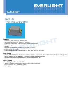
This document details the specifications for a surface-mount Deep Red LED in the compact 17-21 package. This component is designed for modern electronic assembly, offering a significant reduction in size and weight compared to traditional lead-frame LEDs. Its primary advantages include enabling smaller printed circuit board (PCB) designs, higher component packing density, and ultimately contributing to more compact and lightweight end-user equipment.
1.1 Core Features and Compliance
The LED is supplied on 8mm tape wound onto a 7-inch diameter reel, making it fully compatible with automated pick-and-place assembly equipment. It is qualified for use with both infrared (IR) and vapor phase reflow soldering processes. The device is a mono-color type, emitting a deep red light. It is constructed using Pb-free materials and is compliant with key environmental and safety regulations, including the EU RoHS directive, EU REACH regulations, and halogen-free requirements (Br <900 ppm, Cl <900 ppm, Br+Cl < 1500 ppm).
1.2 Target Applications
This LED is suitable for a variety of indicator and backlighting applications. Common uses include backlighting for instrument panel dashboards and switches, status indicators and keypad backlighting in telecommunication devices such as telephones and fax machines, flat backlighting for LCDs, and general-purpose indicator applications where a small, reliable red light source is required.
2. Technical Parameters: In-Depth Objective Interpretation
The following sections provide a detailed, objective analysis of the LED's electrical, optical, and thermal characteristics based on the data sheet parameters. All ratings are specified at an ambient temperature (Ta) of 25°C unless otherwise noted.
2.1 Absolute Maximum Ratings
These ratings define the limits beyond which permanent damage to the device may occur. Operation under or at these conditions is not guaranteed and should be avoided in circuit design.
- Reverse Voltage (VR): 5V. Exceeding this voltage in the reverse direction can cause junction breakdown.
- Continuous Forward Current (IF): 25 mA. This is the maximum DC current recommended for reliable long-term operation.
- Peak Forward Current (IFP): 60 mA. This is permissible only under pulsed conditions with a duty cycle of 1/10 at 1 kHz. It is not for continuous use.
- Power Dissipation (Pd): 60 mW. This is the maximum power the package can dissipate without exceeding its thermal limits.
- Electrostatic Discharge (ESD) Human Body Model (HBM): 2000V. This indicates the device's sensitivity to static electricity; proper ESD handling procedures must be followed.
- Operating Temperature (Topr): -40°C to +85°C. The ambient temperature range over which the device is specified to operate.
- Storage Temperature (Tstg): -40°C to +90°C. The temperature range for storing the device when not powered.
- Soldering Temperature (Tsol): For reflow soldering, a peak temperature of 260°C for a maximum of 10 seconds is specified. For hand soldering, the iron tip temperature should not exceed 350°C for a maximum of 3 seconds per terminal.
2.2 Electro-Optical Characteristics
These parameters define the light output and electrical behavior of the LED under normal operating conditions (IF=20mA, Ta=25°C).
- Luminous Intensity (Iv): Ranges from a minimum of 36.00 mcd to a maximum of 90.00 mcd. The typical value is not specified, indicating performance is managed through a binning system (see Section 3).
- Viewing Angle (2θ1/2): The typical full viewing angle at half intensity is 140 degrees, providing a wide emission pattern.
- Peak Wavelength (λp): The typical wavelength at which the optical power output is maximum is 639 nanometers (nm), placing it in the deep red region of the spectrum.
- Dominant Wavelength (λd): The perceived color wavelength ranges from 625.5 nm to 637.5 nm. This is also managed through binning.
- Spectral Bandwidth (Δλ): The typical full width at half maximum (FWHM) of the emission spectrum is 20 nm.
- Forward Voltage (VF): Ranges from 1.75V to 2.35V at 20mA. This parameter is binned.
- Reverse Current (IR): Maximum of 10 μA when a reverse voltage of 5V is applied. The datasheet explicitly notes the device is not designed for reverse operation; this test parameter is for quality assurance only.
Important Notes: The datasheet specifies manufacturing tolerances: Luminous Intensity (±11%), Dominant Wavelength (±1nm), and Forward Voltage (±0.1V). These apply to the binned values.
3. Binning System Explanation
To ensure consistency in mass production, LEDs are sorted (binned) based on key performance parameters. This allows designers to select parts that meet specific brightness and color requirements for their application.
3.1 Luminous Intensity Binning
LEDs are categorized into four bins (N2, P1, P2, Q1) based on their measured luminous intensity at IF=20mA. For example, a Q1 bin LED will have an intensity between 72.00 and 90.00 mcd.
3.2 Dominant Wavelength Binning
The perceived color (hue) is controlled through three wavelength bins (E6, E7, E8). An E6 bin LED has a dominant wavelength between 625.50 nm and 629.50 nm, resulting in a slightly different shade of red compared to an E8 bin (633.50 nm to 637.50 nm).
3.3 Forward Voltage Binning
Forward voltage is binned into three groups (0, 1, 2). This is crucial for designing current-limiting circuits, especially when driving multiple LEDs in series, to ensure uniform current distribution. A bin 0 LED has a VF between 1.75V and 1.95V, while a bin 2 LED is between 2.15V and 2.35V.
4. Performance Curve Analysis
While the provided PDF excerpt indicates a section for "Typical Electro-Optical Characteristics Curves," the specific graphs (e.g., IV curve, relative intensity vs. current, relative intensity vs. temperature, spectral distribution) are not included in the text content. In a complete datasheet, these curves are essential for design. They typically show:
- Forward Current vs. Forward Voltage (IV Curve): Shows the non-linear relationship, helping to determine the dynamic resistance and the necessary drive voltage for a given current.
- Relative Luminous Intensity vs. Forward Current: Demonstrates how light output increases with current, often showing saturation effects at higher currents.
- Relative Luminous Intensity vs. Ambient Temperature: Shows the decrease in light output as the junction temperature rises, which is critical for thermal management.
- Normalized Spectral Distribution: A graph plotting relative intensity against wavelength, visually confirming the peak wavelength (639nm) and spectral bandwidth (20nm).
Designers should consult the full datasheet with graphs to accurately model the LED's behavior under non-standard conditions (different currents or temperatures).
5. Mechanical and Package Information
5.1 Package Dimensions and Polarity
The LED uses the standard 17-21 SMD package footprint. The key dimensions (in millimeters) are critical for PCB land pattern design. The package has a marked cathode for polarity identification. A typical land pattern would have two pads corresponding to the anode and cathode terminals, with the recommended solder pad size and spacing to ensure proper soldering and mechanical stability. The exact dimensions should be taken from the "Package Dimension" drawing in the datasheet.
5.2 Moisture Sensitivity and Packaging
The device is packaged in a moisture-resistant barrier bag with desiccant to prevent absorption of atmospheric moisture, which can cause "popcorning" (package cracking) during the high-temperature reflow soldering process. The label on the bag contains crucial information for traceability and application: Customer Product Number (CPN), Product Number (P/N), Packing Quantity (QTY), and the specific bin codes for Luminous Intensity (CAT), Dominant Wavelength (HUE), and Forward Voltage (REF).
5.3 Reel and Tape Specifications
The components are supplied on embossed carrier tape wound onto a 7-inch reel. The tape dimensions (pocket size, pitch) and reel dimensions (hub diameter, flange diameter) are standardized to be compatible with automated assembly equipment. The loaded quantity is specified as 3000 pieces per reel.
6. Soldering and Assembly Guidelines
Adherence to these guidelines is critical for assembly yield and long-term reliability.
6.1 Storage and Handling
- Do not open the moisture-proof bag until ready for use.
- After opening, unused LEDs should be stored at ≤30°C and ≤60% Relative Humidity (RH).
- The "floor life" after bag opening is 168 hours (7 days). Unused parts after this period must be re-baked (60±5°C for 24 hours) and re-bagged with fresh desiccant before use.
- Always follow ESD (Electrostatic Discharge) safe handling procedures.
6.2 Reflow Soldering Profile
A Pb-free reflow profile is specified. Key parameters include:
- Pre-heating: 150-200°C for 60-120 seconds.
- Time Above Liquidus (217°C): 60-150 seconds.
- Peak Temperature: Maximum of 260°C.
- Time Within 5°C of Peak: Maximum of 10 seconds.
- Maximum Ramp-Up Rate: 6°C/second.
- Time Above 255°C: Maximum of 30 seconds.
- Maximum Cooling Rate: 3°C/second.
Critical Rule: Reflow soldering should not be performed more than two times on the same LED.
6.3 Hand Soldering and Rework
If hand soldering is unavoidable, use a soldering iron with a tip temperature ≤350°C and apply heat to each terminal for ≤3 seconds. Use a low-power iron (≤25W) and allow a cooling interval of ≥2 seconds between terminals. The datasheet strongly discourages rework after the LED is soldered. If absolutely necessary, a specialized double-head soldering iron must be used to simultaneously heat both terminals during removal to avoid mechanical stress, and the effect on LED characteristics must be verified.
7. Application Suggestions and Design Considerations
7.1 Current Limiting is Mandatory
LEDs are current-driven devices. The datasheet explicitly warns that a series current-limiting resistor must be used. The forward voltage has a negative temperature coefficient and a small variation can cause a large change in current due to the diode's exponential IV characteristic, potentially leading to thermal runaway and failure.
7.2 Thermal Management
While the package is small, the 60mW power dissipation limit must be respected. Operating at high ambient temperatures or high currents will reduce light output and lifespan. Ensure adequate PCB copper area or thermal vias are used if operating near maximum ratings.
7.3 Optical Design
The 140° viewing angle provides a wide, diffuse light pattern suitable for area illumination or indicators that need to be visible from various angles. For more focused light, external lenses or reflectors would be required.
8. Technical Comparison and Differentiation
The primary differentiator of this 17-21 Deep Red LED is its combination of a specific semiconductor material (AIGaInP) and a very compact surface-mount package.
- vs. Older Through-Hole LEDs: Offers massive space savings, weight reduction, and compatibility with high-speed automated assembly, leading to lower overall manufacturing cost.
- vs. Other SMD Red LEDs: The use of AIGaInP technology typically offers higher efficiency and better performance stability over temperature compared to some other material systems for red emission. The specific 639nm peak/deep red color may be chosen for its visual distinctiveness or its effectiveness in certain sensor applications.
- vs. Larger SMD Packages (e.g., 3528, 5050): The 17-21 package is significantly smaller, enabling ultra-miniaturized designs but generally at a lower total light output due to its smaller die size and thermal limits.
8.1 Principle of Operation
Light is produced through a process called electroluminescence within the AIGaInP (Aluminum Gallium Indium Phosphide) semiconductor chip. When a forward voltage is applied, electrons and holes are injected into the active region of the semiconductor junction. When these charge carriers recombine, they release energy in the form of photons (light). The specific composition of the AIGaInP alloy determines the bandgap energy, which directly defines the wavelength (color) of the emitted light—in this case, deep red at approximately 639 nm.
9. Frequently Asked Questions (Based on Technical Parameters)
Q: Can I drive this LED directly from a 3.3V or 5V logic supply?
A: No. You must always use a series current-limiting resistor. The required resistor value is calculated using Ohm's Law: R = (V_supply - VF_LED) / I_desired. Using the maximum VF (2.35V) for a conservative design with a 3.3V supply and 20mA target: R = (3.3 - 2.35) / 0.02 = 47.5Ω. A standard 47Ω or 51Ω resistor would be appropriate.
Q: Why is the luminous intensity given as a range with bins?
A: Due to inherent variations in the semiconductor manufacturing process, individual LEDs have slightly different performances. Binning sorts them into groups with guaranteed minimum and maximum values, allowing designers to select the appropriate brightness grade for their cost and performance needs.
Q: What happens if I exceed the 7-day floor life after opening the bag?
A: The absorbed moisture can turn to steam during reflow, potentially causing internal delamination or cracking. The parts must be reconditioned by baking at 60°C for 24 hours before use.
Q: Is this LED suitable for automotive dashboard lighting?
A> While "dashboard backlighting" is listed as an application, the datasheet includes an "Application Restrictions" section. It cautions that high-reliability applications like automotive safety/security systems may require a different, more rigorously qualified product. For non-critical dashboard illumination, it may be suitable, but for safety-critical indicators, a product specifically qualified to automotive standards (e.g., AEC-Q102) should be sourced.
10. Practical Design and Usage Case
Scenario: Designing a compact status indicator panel. A designer needs multiple deep red status LEDs on a densely populated control board. They select this 17-21 LED for its small size. They specify the Q1 brightness bin and E7 wavelength bin to ensure bright, consistent color across all indicators. On the PCB layout, they use the recommended land pattern from the datasheet. They design the drive circuit using a 3.3V regulator, a 51Ω current-limiting resistor for each LED (resulting in ~18-20mA), and place small thermal relief pads. During assembly, they ensure the factory-sealed reel is used within the floor life and follow the specified reflow profile. This results in a reliable, compact indicator system.
11. Technology Trends
The general trend in LED technology, including for indicators, is towards several key areas:
- Increased Efficiency: Ongoing material science improvements aim to produce more light (lumens) per unit of electrical input power (watts), reducing energy consumption and thermal load.
- Miniaturization: Packages continue to shrink (e.g., from 17-21 to even smaller footprints like 10-05) to enable ever-smaller electronic devices.
- Higher Reliability and Robustness: Improvements in packaging materials and die attach technologies enhance lifespan and resistance to thermal cycling and moisture.
- Integration: There is a trend towards integrating multiple LEDs (e.g., RGB), control ICs, and even passive components into single, smarter module packages.
- Standardization and Compliance: Stricter and more widespread environmental regulations (RoHS, REACH, halogen-free) continue to drive material changes across the industry.
LED Specification Terminology
Complete explanation of LED technical terms
Photoelectric Performance
| Term | Unit/Representation | Simple Explanation | Why Important |
|---|---|---|---|
| Luminous Efficacy | lm/W (lumens per watt) | Light output per watt of electricity, higher means more energy efficient. | Directly determines energy efficiency grade and electricity cost. |
| Luminous Flux | lm (lumens) | Total light emitted by source, commonly called "brightness". | Determines if the light is bright enough. |
| Viewing Angle | ° (degrees), e.g., 120° | Angle where light intensity drops to half, determines beam width. | Affects illumination range and uniformity. |
| CCT (Color Temperature) | K (Kelvin), e.g., 2700K/6500K | Warmth/coolness of light, lower values yellowish/warm, higher whitish/cool. | Determines lighting atmosphere and suitable scenarios. |
| CRI / Ra | Unitless, 0–100 | Ability to render object colors accurately, Ra≥80 is good. | Affects color authenticity, used in high-demand places like malls, museums. |
| SDCM | MacAdam ellipse steps, e.g., "5-step" | Color consistency metric, smaller steps mean more consistent color. | Ensures uniform color across same batch of LEDs. |
| Dominant Wavelength | nm (nanometers), e.g., 620nm (red) | Wavelength corresponding to color of colored LEDs. | Determines hue of red, yellow, green monochrome LEDs. |
| Spectral Distribution | Wavelength vs intensity curve | Shows intensity distribution across wavelengths. | Affects color rendering and quality. |
Electrical Parameters
| Term | Symbol | Simple Explanation | Design Considerations |
|---|---|---|---|
| Forward Voltage | Vf | Minimum voltage to turn on LED, like "starting threshold". | Driver voltage must be ≥Vf, voltages add up for series LEDs. |
| Forward Current | If | Current value for normal LED operation. | Usually constant current drive, current determines brightness & lifespan. |
| Max Pulse Current | Ifp | Peak current tolerable for short periods, used for dimming or flashing. | Pulse width & duty cycle must be strictly controlled to avoid damage. |
| Reverse Voltage | Vr | Max reverse voltage LED can withstand, beyond may cause breakdown. | Circuit must prevent reverse connection or voltage spikes. |
| Thermal Resistance | Rth (°C/W) | Resistance to heat transfer from chip to solder, lower is better. | High thermal resistance requires stronger heat dissipation. |
| ESD Immunity | V (HBM), e.g., 1000V | Ability to withstand electrostatic discharge, higher means less vulnerable. | Anti-static measures needed in production, especially for sensitive LEDs. |
Thermal Management & Reliability
| Term | Key Metric | Simple Explanation | Impact |
|---|---|---|---|
| Junction Temperature | Tj (°C) | Actual operating temperature inside LED chip. | Every 10°C reduction may double lifespan; too high causes light decay, color shift. |
| Lumen Depreciation | L70 / L80 (hours) | Time for brightness to drop to 70% or 80% of initial. | Directly defines LED "service life". |
| Lumen Maintenance | % (e.g., 70%) | Percentage of brightness retained after time. | Indicates brightness retention over long-term use. |
| Color Shift | Δu′v′ or MacAdam ellipse | Degree of color change during use. | Affects color consistency in lighting scenes. |
| Thermal Aging | Material degradation | Deterioration due to long-term high temperature. | May cause brightness drop, color change, or open-circuit failure. |
Packaging & Materials
| Term | Common Types | Simple Explanation | Features & Applications |
|---|---|---|---|
| Package Type | EMC, PPA, Ceramic | Housing material protecting chip, providing optical/thermal interface. | EMC: good heat resistance, low cost; Ceramic: better heat dissipation, longer life. |
| Chip Structure | Front, Flip Chip | Chip electrode arrangement. | Flip chip: better heat dissipation, higher efficacy, for high-power. |
| Phosphor Coating | YAG, Silicate, Nitride | Covers blue chip, converts some to yellow/red, mixes to white. | Different phosphors affect efficacy, CCT, and CRI. |
| Lens/Optics | Flat, Microlens, TIR | Optical structure on surface controlling light distribution. | Determines viewing angle and light distribution curve. |
Quality Control & Binning
| Term | Binning Content | Simple Explanation | Purpose |
|---|---|---|---|
| Luminous Flux Bin | Code e.g., 2G, 2H | Grouped by brightness, each group has min/max lumen values. | Ensures uniform brightness in same batch. |
| Voltage Bin | Code e.g., 6W, 6X | Grouped by forward voltage range. | Facilitates driver matching, improves system efficiency. |
| Color Bin | 5-step MacAdam ellipse | Grouped by color coordinates, ensuring tight range. | Guarantees color consistency, avoids uneven color within fixture. |
| CCT Bin | 2700K, 3000K etc. | Grouped by CCT, each has corresponding coordinate range. | Meets different scene CCT requirements. |
Testing & Certification
| Term | Standard/Test | Simple Explanation | Significance |
|---|---|---|---|
| LM-80 | Lumen maintenance test | Long-term lighting at constant temperature, recording brightness decay. | Used to estimate LED life (with TM-21). |
| TM-21 | Life estimation standard | Estimates life under actual conditions based on LM-80 data. | Provides scientific life prediction. |
| IESNA | Illuminating Engineering Society | Covers optical, electrical, thermal test methods. | Industry-recognized test basis. |
| RoHS / REACH | Environmental certification | Ensures no harmful substances (lead, mercury). | Market access requirement internationally. |
| ENERGY STAR / DLC | Energy efficiency certification | Energy efficiency and performance certification for lighting. | Used in government procurement, subsidy programs, enhances competitiveness. |