Table of Contents
- 1. Product Overview
- 2. Technical Parameter Deep Dive
- 2.1 Absolute Maximum Ratings
- 2.2 Electro-Optical Characteristics
- 3. Binning System Explanation
- 3.1 Luminous Intensity Binning
- 3.2 Dominant Wavelength Binning
- 3.3 Forward Voltage Binning
- 4. Performance Curve Analysis
- 5. Mechanical and Package Information
- 5.1 Package Dimensions
- 5.2 Polarity Identification
- 6. Soldering and Assembly Guidelines
- 6.1 Reflow Soldering Profile
- 6.2 Hand Soldering
- 6.3 Storage and Handling
- 6.4 Precautions
- 7. Packaging and Ordering Information
- 8. Application Recommendations
- 8.1 Typical Application Scenarios
- 8.2 Design Considerations
- 9. Technical Comparison and Differentiation
- 10. Frequently Asked Questions (FAQ)
- 11. Practical Design and Usage Case
- 12. Operating Principle Introduction
- 13. Technology Trends and Developments
1. Product Overview
The 17-21 SMD LED is a compact, surface-mount device designed for high-density electronic assemblies. Its primary function is to emit pure green light, making it suitable for a variety of indicator and backlighting applications. The core advantage of this component lies in its miniature footprint, which enables significant reductions in board size and equipment dimensions. The lightweight construction further enhances its suitability for space-constrained and portable devices. The product is fully compliant with modern environmental standards, being Pb-free, RoHS compliant, REACH compliant, and Halogen-Free, ensuring its use in global markets with strict regulatory requirements.
2. Technical Parameter Deep Dive
2.1 Absolute Maximum Ratings
The device is rated for a maximum reverse voltage (VR) of 5V. The continuous forward current (IF) should not exceed 25mA, while a peak forward current (IFP) of 60mA is permissible under pulsed conditions (duty cycle 1/10 at 1kHz). The maximum power dissipation (Pd) is 60mW. The operating temperature range is specified from -40°C to +85°C, with a storage temperature range from -40°C to +90°C. The LED can withstand reflow soldering at 260°C for up to 10 seconds or hand soldering at 350°C for up to 3 seconds.
2.2 Electro-Optical Characteristics
Under standard test conditions (Ta=25°C, IF=20mA), the luminous intensity (Iv) ranges from a minimum of 7.20 mcd to a maximum of 22.50 mcd. The device features a wide viewing angle (2θ1/2) of 140 degrees, providing broad illumination. The peak wavelength (λp) is 561 nm, with a dominant wavelength (λd) range between 557.50 nm and 567.50 nm, defining its pure green color. The spectral bandwidth (Δλ) is typically 20 nm. The forward voltage (VF) ranges from 1.55V to 2.35V at the test current. The reverse current (IR) is a maximum of 10 μA when a 5V reverse bias is applied, though the device is not designed for reverse operation.
3. Binning System Explanation
The product is categorized into bins for key parameters to ensure consistency in application design.
3.1 Luminous Intensity Binning
Luminous intensity is sorted into four bin codes: K0 (7.20-11.50 mcd), L1 (11.50-14.50 mcd), L2 (14.50-18.00 mcd), and M1 (18.00-22.50 mcd). A tolerance of ±11% applies.
3.2 Dominant Wavelength Binning
Dominant wavelength is sorted into five bin codes: C10 (557.50-559.50 nm), C11 (559.50-561.50 nm), C12 (561.50-563.50 nm), C13 (563.50-565.50 nm), and C14 (565.50-567.50 nm). A tolerance of ±1nm applies.
3.3 Forward Voltage Binning
Forward voltage is sorted into three bin codes: 0 (1.75-1.95 V), 1 (1.95-2.15 V), and 2 (2.15-2.35 V). A tolerance of ±0.1V applies.
4. Performance Curve Analysis
While specific graphical curves are referenced in the datasheet, typical performance trends can be inferred from the parameters. The forward voltage will exhibit a logarithmic relationship with forward current. Luminous intensity is directly proportional to forward current within the specified limits but will decrease with increasing junction temperature. The dominant wavelength may experience a slight shift (typically towards longer wavelengths) as the junction temperature rises. Understanding these relationships is crucial for designing stable and efficient driver circuits.
5. Mechanical and Package Information
5.1 Package Dimensions
The 17-21 SMD LED has a compact package with dimensions of approximately 1.6mm in length, 0.8mm in width, and 0.6mm in height (tolerance ±0.1mm). The package includes a clear cathode mark for correct polarity identification during assembly. The detailed dimensional drawing provides exact measurements for pad layout design to ensure proper soldering and thermal management.
5.2 Polarity Identification
A distinct mark on the package body indicates the cathode terminal. Correct orientation is essential for circuit functionality and to prevent damage from reverse bias.
6. Soldering and Assembly Guidelines
6.1 Reflow Soldering Profile
For Pb-free soldering, a specific temperature profile must be followed: pre-heating between 150-200°C for 60-120 seconds, time above 217°C for 60-150 seconds, peak temperature at 260°C maximum for 10 seconds maximum, with controlled heating and cooling rates (6°C/sec max heating above 255°C, 3°C/sec max cooling). Reflow soldering should not be performed more than twice.
6.2 Hand Soldering
If hand soldering is necessary, the iron tip temperature must be below 350°C, applied for no more than 3 seconds per terminal. Use a soldering iron with a capacity of 25W or less. Allow an interval of at least 2 seconds between soldering each terminal to prevent thermal damage.
6.3 Storage and Handling
The LEDs are packaged in moisture-resistant bags with desiccant. The bag must not be opened until the components are ready for use. After opening, unused LEDs should be stored at ≤30°C and ≤60% RH and used within 168 hours (7 days). If this window is exceeded or the desiccant indicator changes color, a baking treatment at 60±5°C for 24 hours is required before use.
6.4 Precautions
An external current-limiting resistor is mandatory for operation, as the LED's exponential I-V characteristic makes it highly sensitive to voltage variations, which can lead to overcurrent and failure. Avoid applying mechanical stress to the LED during heating or bending the PCB after soldering. Repair after soldering is not recommended, but if unavoidable, a specialized double-head soldering iron should be used to simultaneously heat both terminals, minimizing thermal stress.
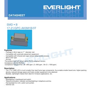
7. Packaging and Ordering Information
The LEDs are supplied on 8mm wide carrier tape, wound onto 7-inch diameter reels. Each reel contains 3000 pieces. The packaging includes moisture-proof aluminum bags with desiccant and labels. The label contains key information: Customer's Product Number (CPN), Product Number (P/N), Packing Quantity (QTY), Luminous Intensity Rank (CAT), Chromaticity/Dominant Wavelength Rank (HUE), Forward Voltage Rank (REF), and Lot Number (LOT No).
8. Application Recommendations
8.1 Typical Application Scenarios
This LED is well-suited for backlighting applications in automotive dashboards and switches. In telecommunications, it serves as status indicators and keypad backlights in phones and fax machines. It is also applicable for flat backlighting of LCDs, switches, and symbols, as well as general-purpose indicator use.
8.2 Design Considerations
Designers must incorporate a suitable current-limiting resistor in series with the LED. The resistor value should be calculated based on the supply voltage, the forward voltage bin of the LED (using the maximum value for safety), and the desired operating current (≤20mA for continuous operation). Consider the luminous intensity bin when designing for required brightness levels. Ensure the PCB pad layout matches the package dimensions to prevent tombstoning or poor solder joints.
9. Technical Comparison and Differentiation
The primary differentiation of the 17-21 LED is its extremely small form factor (1.6x0.8mm) compared to traditional leaded LEDs, enabling higher packing density. The use of an AIGaInP chip material provides efficient pure green emission. The wide 140-degree viewing angle offers more uniform illumination compared to narrower-angle devices. Its full compliance with Pb-free, RoHS, REACH, and Halogen-Free standards makes it a future-proof choice for global electronics manufacturing.
10. Frequently Asked Questions (FAQ)
Q: What is the purpose of the binning codes?
A: Binning ensures electrical and optical consistency within a batch. Designers can select specific bins (e.g., for brightness or voltage) to achieve uniform performance in their end products, especially when multiple LEDs are used in an array.
Q: Why is a current-limiting resistor mandatory?
A: LEDs are diodes with a non-linear I-V curve. A small increase in voltage beyond the forward voltage can cause a large, potentially destructive increase in current. A series resistor provides a linear, predictable method to set the operating current.
Q: Can I use this LED for automotive exterior lighting?
A: No. The datasheet includes an application restriction stating that this product is not intended for high-reliability applications like automotive safety/security systems, military/aerospace, or medical equipment without prior consultation and qualification.
Q: How many times can I reflow solder this component?
A: The maximum recommended is two reflow cycles. Each cycle subjects the component to thermal stress, which can degrade internal materials and solder joint integrity over time.
11. Practical Design and Usage Case
Consider designing a low-power status indicator panel for a consumer device. Using the 17-21 LED in bin M1 (highest brightness) and bin C12 (specific green hue), a designer can create a uniform, bright display. By calculating the series resistor for a 3.3V supply (R = (3.3V - 2.35V) / 0.02A ≈ 47.5Ω, use 47Ω), they ensure stable operation at ~20mA. The LEDs would be placed on tape and reel for automated pick-and-place assembly, following the specified reflow profile. The final panel benefits from the LED's small size, allowing for a sleek design, and its wide viewing angle ensures the indicator is visible from various positions.
12. Operating Principle Introduction
This LED operates on the principle of electroluminescence in a semiconductor p-n junction. The chip material is Aluminum Indium Gallium Phosphide (AIGaInP). When a forward voltage exceeding the junction's built-in potential is applied, electrons and holes are injected across the junction. Their recombination releases energy in the form of photons (light). The specific bandgap energy of the AIGaInP alloy determines the wavelength of the emitted light, in this case, pure green (~561 nm). The clear resin encapsulant protects the chip and acts as a lens, shaping the light output to achieve the specified 140-degree viewing angle.
13. Technology Trends and Developments
The trend in SMD LEDs like the 17-21 continues towards higher efficiency (more lumens per watt), smaller package sizes for increased density, and improved color consistency and stability over temperature and lifetime. There is also a strong drive for broader adoption of environmentally friendly materials and manufacturing processes, as evidenced by this product's compliance with multiple green standards. Integration with intelligent drivers and controls for smart lighting applications is another growing area, though at the component level, the focus remains on providing reliable, high-performance light sources for increasingly miniaturized and power-sensitive electronic devices.
LED Specification Terminology
Complete explanation of LED technical terms
Photoelectric Performance
| Term | Unit/Representation | Simple Explanation | Why Important |
|---|---|---|---|
| Luminous Efficacy | lm/W (lumens per watt) | Light output per watt of electricity, higher means more energy efficient. | Directly determines energy efficiency grade and electricity cost. |
| Luminous Flux | lm (lumens) | Total light emitted by source, commonly called "brightness". | Determines if the light is bright enough. |
| Viewing Angle | ° (degrees), e.g., 120° | Angle where light intensity drops to half, determines beam width. | Affects illumination range and uniformity. |
| CCT (Color Temperature) | K (Kelvin), e.g., 2700K/6500K | Warmth/coolness of light, lower values yellowish/warm, higher whitish/cool. | Determines lighting atmosphere and suitable scenarios. |
| CRI / Ra | Unitless, 0–100 | Ability to render object colors accurately, Ra≥80 is good. | Affects color authenticity, used in high-demand places like malls, museums. |
| SDCM | MacAdam ellipse steps, e.g., "5-step" | Color consistency metric, smaller steps mean more consistent color. | Ensures uniform color across same batch of LEDs. |
| Dominant Wavelength | nm (nanometers), e.g., 620nm (red) | Wavelength corresponding to color of colored LEDs. | Determines hue of red, yellow, green monochrome LEDs. |
| Spectral Distribution | Wavelength vs intensity curve | Shows intensity distribution across wavelengths. | Affects color rendering and quality. |
Electrical Parameters
| Term | Symbol | Simple Explanation | Design Considerations |
|---|---|---|---|
| Forward Voltage | Vf | Minimum voltage to turn on LED, like "starting threshold". | Driver voltage must be ≥Vf, voltages add up for series LEDs. |
| Forward Current | If | Current value for normal LED operation. | Usually constant current drive, current determines brightness & lifespan. |
| Max Pulse Current | Ifp | Peak current tolerable for short periods, used for dimming or flashing. | Pulse width & duty cycle must be strictly controlled to avoid damage. |
| Reverse Voltage | Vr | Max reverse voltage LED can withstand, beyond may cause breakdown. | Circuit must prevent reverse connection or voltage spikes. |
| Thermal Resistance | Rth (°C/W) | Resistance to heat transfer from chip to solder, lower is better. | High thermal resistance requires stronger heat dissipation. |
| ESD Immunity | V (HBM), e.g., 1000V | Ability to withstand electrostatic discharge, higher means less vulnerable. | Anti-static measures needed in production, especially for sensitive LEDs. |
Thermal Management & Reliability
| Term | Key Metric | Simple Explanation | Impact |
|---|---|---|---|
| Junction Temperature | Tj (°C) | Actual operating temperature inside LED chip. | Every 10°C reduction may double lifespan; too high causes light decay, color shift. |
| Lumen Depreciation | L70 / L80 (hours) | Time for brightness to drop to 70% or 80% of initial. | Directly defines LED "service life". |
| Lumen Maintenance | % (e.g., 70%) | Percentage of brightness retained after time. | Indicates brightness retention over long-term use. |
| Color Shift | Δu′v′ or MacAdam ellipse | Degree of color change during use. | Affects color consistency in lighting scenes. |
| Thermal Aging | Material degradation | Deterioration due to long-term high temperature. | May cause brightness drop, color change, or open-circuit failure. |
Packaging & Materials
| Term | Common Types | Simple Explanation | Features & Applications |
|---|---|---|---|
| Package Type | EMC, PPA, Ceramic | Housing material protecting chip, providing optical/thermal interface. | EMC: good heat resistance, low cost; Ceramic: better heat dissipation, longer life. |
| Chip Structure | Front, Flip Chip | Chip electrode arrangement. | Flip chip: better heat dissipation, higher efficacy, for high-power. |
| Phosphor Coating | YAG, Silicate, Nitride | Covers blue chip, converts some to yellow/red, mixes to white. | Different phosphors affect efficacy, CCT, and CRI. |
| Lens/Optics | Flat, Microlens, TIR | Optical structure on surface controlling light distribution. | Determines viewing angle and light distribution curve. |
Quality Control & Binning
| Term | Binning Content | Simple Explanation | Purpose |
|---|---|---|---|
| Luminous Flux Bin | Code e.g., 2G, 2H | Grouped by brightness, each group has min/max lumen values. | Ensures uniform brightness in same batch. |
| Voltage Bin | Code e.g., 6W, 6X | Grouped by forward voltage range. | Facilitates driver matching, improves system efficiency. |
| Color Bin | 5-step MacAdam ellipse | Grouped by color coordinates, ensuring tight range. | Guarantees color consistency, avoids uneven color within fixture. |
| CCT Bin | 2700K, 3000K etc. | Grouped by CCT, each has corresponding coordinate range. | Meets different scene CCT requirements. |
Testing & Certification
| Term | Standard/Test | Simple Explanation | Significance |
|---|---|---|---|
| LM-80 | Lumen maintenance test | Long-term lighting at constant temperature, recording brightness decay. | Used to estimate LED life (with TM-21). |
| TM-21 | Life estimation standard | Estimates life under actual conditions based on LM-80 data. | Provides scientific life prediction. |
| IESNA | Illuminating Engineering Society | Covers optical, electrical, thermal test methods. | Industry-recognized test basis. |
| RoHS / REACH | Environmental certification | Ensures no harmful substances (lead, mercury). | Market access requirement internationally. |
| ENERGY STAR / DLC | Energy efficiency certification | Energy efficiency and performance certification for lighting. | Used in government procurement, subsidy programs, enhances competitiveness. |