Table of Contents
- 1. Product Overview
- 1.1 Core Features and Compliance
- 1.2 Target Applications
- 2. Technical Specifications Deep Dive
- 2.1 Absolute Maximum Ratings
- 2.2 Electro-Optical Characteristics
- 3. Binning System Explanation
- 3.1 Luminous Intensity Binning
- 3.2 Forward Voltage Binning
- 3.3 Chromaticity Coordinate Binning
- 4. Performance Curve Analysis
- 4.1 Forward Current vs. Forward Voltage (I-V Curve)
- 4.2 Relative Luminous Intensity vs. Forward Current
- 4.3 Relative Luminous Intensity vs. Ambient Temperature
- 4.4 Forward Current Derating Curve
- 4.5 Spectrum Distribution
- 4.6 Radiation Pattern
- 5. Mechanical and Package Information
- 5.1 Package Dimensions
- 5.2 Polarity Identification
- 6. Soldering and Assembly Guidelines
- 6.1 Current Limiting Requirement
- 6.2 Storage and Moisture Sensitivity
- 6.3 Reflow Soldering Profile
- 7. Packaging and Ordering Information
- 7.1 Reel and Tape Specifications
- 7.2 Label Explanation
- 8. Application Design Considerations
- 8.1 Driving Circuit Design
- 8.2 Thermal Management
- 8.3 Optical Integration
- 9. Technical Comparison and Positioning
- 10. Frequently Asked Questions (FAQ)
- 10.1 What resistor do I need for a 3.3V supply?
- 10.2 Can I drive it with a PWM signal for dimming?
- 10.3 Why is the luminous intensity given in mcd instead of lumens?
- 10.4 What does the "T1D" in the part number signify?
- 11. Design-in Case Study: Dashboard Switch Backlighting
- 12. Technology Principle
- 13. Industry Trends
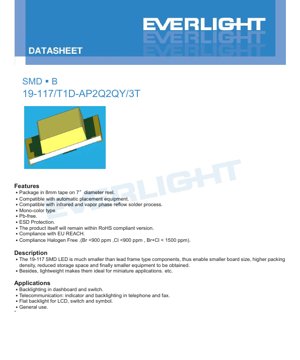
1. Product Overview
This document details the specifications for a surface-mount device (SMD) LED identified as 19-117/T1D-AP2Q2QY/3T. This component is a mono-color, pure white LED designed for modern electronic assembly processes. Its compact SMD package offers significant advantages over traditional lead-frame components, enabling the design of smaller printed circuit boards (PCBs), higher component packing density, and ultimately more compact end-user equipment. The lightweight nature of the package further makes it suitable for miniature and portable applications.
1.1 Core Features and Compliance
The LED is supplied on 8mm tape wound onto a 7-inch diameter reel, making it fully compatible with standard automated pick-and-place equipment for high-volume manufacturing. It is designed to be processed using both infrared and vapor phase reflow soldering techniques. The device is constructed using lead-free (Pb-free) materials and incorporates Electrostatic Discharge (ESD) protection. It complies with key environmental and safety regulations, including the EU's RoHS (Restriction of Hazardous Substances) directive, REACH (Registration, Evaluation, Authorisation and Restriction of Chemicals) regulation, and is classified as Halogen-Free, with Bromine (Br) and Chlorine (Cl) content below 900 ppm each and their sum below 1500 ppm.
1.2 Target Applications
This LED is versatile and finds use in various illumination and indication roles. Primary applications include backlighting for instrument panel dashboards and membrane switches. In telecommunications equipment, it can serve as status indicators or backlights for devices like telephones and fax machines. It is also suitable for providing flat backlighting for liquid crystal displays (LCDs), switch panels, and symbols. Its general-purpose nature allows for use in a wide array of consumer and industrial electronics where a compact, reliable white light source is required.
2. Technical Specifications Deep Dive
This section provides a detailed analysis of the electrical, optical, and thermal limits and characteristics of the LED. Understanding these parameters is crucial for reliable circuit design and ensuring long-term performance.
2.1 Absolute Maximum Ratings
The Absolute Maximum Ratings define the stress limits beyond which permanent damage to the device may occur. These ratings are specified at an ambient temperature (Ta) of 25\u00b0C and must not be exceeded under any operating conditions. The key limits are:
- Reverse Voltage (VR): 5V. Applying a reverse bias voltage higher than this can break down the LED's semiconductor junction.
- Continuous Forward Current (IF): 10mA. This is the maximum DC current that can be passed through the LED continuously.
- Peak Forward Current (IFP): 100mA. This is the maximum allowable pulsed current, specified at a duty cycle of 1/10 and a frequency of 1 kHz. It is suitable for brief, high-intensity flashes.
- Power Dissipation (Pd): 40mW. This is the maximum amount of power the device can dissipate as heat, calculated as Forward Voltage (VF) \u00d7 Forward Current (IF).
- ESD Withstand (HBM): 2000V. The device can withstand electrostatic discharge up to this level per the Human Body Model (HBM), indicating good handling robustness.
- Operating Temperature (Topr): -40\u00b0C to +85\u00b0C. The ambient temperature range over which the LED is designed to function.
- Storage Temperature (Tstg): -40\u00b0C to +90\u00b0C. The temperature range for storing the device when not powered.
- Soldering Temperature: The package can withstand reflow soldering with a peak temperature of 260\u00b0C for up to 10 seconds, or hand soldering at 350\u00b0C for up to 3 seconds.
2.2 Electro-Optical Characteristics
The Electro-Optical Characteristics are measured at Ta=25\u00b0C and a standard test current (IF) of 5mA. These represent the typical performance parameters.
- Luminous Intensity (Iv): The light output ranges from a minimum of 57.0 millicandelas (mcd) to a maximum of 112.0 mcd. The typical value falls within this range, and specific bins are defined (see Section 3). The tolerance is \u00b111%.
- Viewing Angle (2\u03b81/2): The typical viewing angle, defined as the angle where intensity drops to half of its peak value, is 130 degrees. This indicates a wide, diffuse emission pattern suitable for area illumination.
- Forward Voltage (VF): The voltage drop across the LED when conducting 5mA typically ranges from 2.70V to 3.20V. The tolerance is \u00b10.05V. This parameter is critical for designing the current-limiting circuitry.
3. Binning System Explanation
To ensure consistency in mass production, LEDs are sorted into "bins" based on key performance parameters. This allows designers to select parts that meet specific brightness and electrical requirements for their application.
3.1 Luminous Intensity Binning
The luminous output is categorized into three bins (P2, Q1, Q2) when measured at IF=5mA:
- Bin P2: 57.0 mcd (Min) to 72.0 mcd (Max)
- Bin Q1: 72.0 mcd (Min) to 90.0 mcd (Max)
- Bin Q2: 90.0 mcd (Min) to 112.0 mcd (Max)
The specific bin code (e.g., Q2 in the part number 19-117/T1D-AP2Q2QY/3T) indicates the guaranteed minimum light output for that particular unit.
3.2 Forward Voltage Binning
The forward voltage is categorized into five bins (29 to 33) at IF=5mA:
- Bin 29: 2.70V to 2.80V
- Bin 30: 2.80V to 2.90V
- Bin 31: 2.90V to 3.00V
- Bin 32: 3.00V to 3.10V
- Bin 33: 3.10V to 3.20V
This binning helps in designing power supplies and predicting current draw more accurately across a batch of LEDs.
3.3 Chromaticity Coordinate Binning
The color of the white light is defined by its chromaticity coordinates (x, y) on the CIE 1931 diagram. The datasheet defines six bins (1 through 6), each specifying a quadrilateral area on the color chart. The coordinates for the four corners of each bin are provided. This ensures the emitted white light falls within a specific, controlled color space. The tolerance for these coordinates is \u00b10.01.
4. Performance Curve Analysis
Graphical data provides deeper insight into the LED's behavior under varying conditions.
4.1 Forward Current vs. Forward Voltage (I-V Curve)
The I-V curve shows the exponential relationship between current and voltage. For this LED, at a fixed ambient temperature of 25\u00b0C, the forward voltage increases as the current increases. This curve is essential for determining the operating point and the necessary series resistor value to achieve a desired current.
4.2 Relative Luminous Intensity vs. Forward Current
This graph demonstrates how light output increases with forward current. It typically shows a near-linear relationship at lower currents, which may saturate at higher currents due to thermal and efficiency effects. The curve is plotted on a semi-log scale, showing intensity from 10% to 1000% relative to a baseline.
4.3 Relative Luminous Intensity vs. Ambient Temperature
LED efficiency decreases as junction temperature rises. This curve plots the relative light output against ambient temperature (Ta). It typically shows a peak near room temperature, with output declining as temperature increases or decreases significantly. This is critical for applications operating in non-ideal thermal environments.
4.4 Forward Current Derating Curve
To prevent overheating, the maximum allowable continuous forward current must be reduced as the ambient temperature increases. This derating curve specifies the safe operating current for ambient temperatures above 25\u00b0C up to the maximum operating temperature.
4.5 Spectrum Distribution
The spectral power distribution curve shows the intensity of light emitted at each wavelength. For a white LED based on an InGaN blue chip with a yellow phosphor (as indicated in the Device Selection Guide), the spectrum will typically show a dominant blue peak from the chip and a broader yellow/green emission from the phosphor, combining to produce white light.
4.6 Radiation Pattern
A polar diagram illustrates the spatial distribution of light intensity. The provided diagram, with normalized intensity values at various angles, confirms the wide 130-degree viewing angle, showing a Lambertian or near-Lambertian emission pattern where intensity is highest at 0 degrees (perpendicular to the emitting surface) and decreases towards the sides.
5. Mechanical and Package Information
5.1 Package Dimensions
The datasheet includes a detailed mechanical drawing of the LED package. Key dimensions include the overall length, width, and height, as well as the size and position of the solder pads (anode and cathode). The drawing specifies tolerances, typically \u00b10.1mm unless otherwise noted. Correct interpretation of this drawing is vital for PCB footprint design to ensure proper soldering and alignment.
5.2 Polarity Identification
The package drawing clearly indicates which solder pad corresponds to the anode (positive) and cathode (negative). Incorrect polarity connection will prevent the LED from illuminating and may exceed the reverse voltage rating.
6. Soldering and Assembly Guidelines
6.1 Current Limiting Requirement
Critical: An external current-limiting resistor (or constant-current driver) must be used in series with the LED. The LED's forward voltage has a negative temperature coefficient and a small variation can cause a large change in current due to its diode characteristics. Operating without current control will almost certainly lead to thermal runaway and rapid failure.
6.2 Storage and Moisture Sensitivity
The LEDs are packaged in a moisture-resistant barrier bag with desiccant to prevent absorption of atmospheric moisture, which can cause "popcorning" (package cracking) during reflow soldering.
- Before Opening: Store at \u2264 30\u00b0C and \u2264 90% Relative Humidity (RH).
- After Opening: The "floor life" (time components can be exposed to ambient factory conditions) is 1 year at \u2264 30\u00b0C and \u2264 60% RH. Unused parts should be resealed in a moisture-proof bag with fresh desiccant.
- Baking: If the desiccant indicator shows saturation or the exposure time is exceeded, the components must be baked at 60 \u00b1 5\u00b0C for 24 hours to remove moisture before soldering.
6.3 Reflow Soldering Profile
A recommended Pb-free reflow temperature profile is provided:
- Pre-heating: Ramp from ambient to 150-200\u00b0C over 60-120 seconds.
- Soak/Preflow: Maintain above 217\u00b0C (the melting point of Pb-free solder) for 60-150 seconds.
- Reflow: Peak temperature should not exceed 260\u00b0C, and the time above 255\u00b0C should be limited to 30 seconds maximum. The time at the actual peak should be 10 seconds maximum.
- Cooling: The maximum cooling rate is specified as 6\u00b0C/second.
Important Notes: Reflow soldering should not be performed more than two times. Avoid mechanical stress on the LED during heating, and do not warp the PCB after soldering, as this can damage the solder joints or the component itself.
7. Packaging and Ordering Information
7.1 Reel and Tape Specifications
The LEDs are supplied in embossed carrier tape for automated handling.
- Reel: Standard 7-inch (178mm) diameter reel.
- Tape Width: 8mm.
- Pocket Pitch & Quantity: The carrier tape dimensions are specified to hold 3000 pieces per reel.
- Reel Dimensions: Detailed drawings show the reel hub diameter, flange diameter, and overall width.
7.2 Label Explanation
The packaging label contains several codes:
- CPN: Customer's Product Number (optional).
- P/N: The manufacturer's full part number (e.g., 19-117/T1D-AP2Q2QY/3T).
- QTY: Packing quantity on the reel.
- CAT: Luminous Intensity bin rank (e.g., Q2).
- HUE: Chromaticity coordinate and dominant wavelength rank.
- REF: Forward Voltage bin rank (e.g., 29-33).
- LOT No: Traceability lot number.
8. Application Design Considerations
8.1 Driving Circuit Design
The most common drive method is a series resistor. The resistor value (R) is calculated using Ohm's Law: R = (Vsupply - VF) / IF. Choose VF from the maximum rating or a conservative value from the bin range to ensure current does not exceed limits even with component variations. For example, with a 5V supply and using VF_max of 3.2V for a target IF of 5mA: R = (5V - 3.2V) / 0.005A = 360\u03a9. The nearest standard value (e.g., 390\u03a9) would be selected, resulting in a slightly lower current. For precision or varying supply voltages, constant-current drivers are recommended.
8.2 Thermal Management
While the power dissipation is low (max 40mW), effective thermal management on the PCB is still important for maintaining light output and longevity, especially in high ambient temperatures or when driven near maximum current. Ensure the PCB has adequate copper area connected to the LED's thermal pad (if present) or solder pads to act as a heat sink. Follow the current derating curve for elevated temperature operation.
8.3 Optical Integration
The wide 130-degree viewing angle makes this LED suitable for applications requiring even, diffuse illumination over an area, such as behind a light guide or diffuser panel. For more focused light, external lenses or reflectors would be necessary. The yellow-diffused resin helps in scattering light, contributing to the wide viewing angle.
9. Technical Comparison and Positioning
This LED, based on its parameters, is positioned as a general-purpose, low-power white illumination source. Compared to older through-hole LEDs, its SMD format offers significant space savings and manufacturing efficiency. Within the SMD white LED landscape, its key differentiators are its specific combination of a relatively low forward voltage (compatible with 3.3V logic supplies), moderate luminous intensity suitable for indication and local backlighting, and compliance with modern environmental standards (Halogen-Free, Pb-free). It is not a high-power or high-brightness LED for primary lighting but is optimized for reliable, compact secondary lighting and status indication.
10. Frequently Asked Questions (FAQ)
10.1 What resistor do I need for a 3.3V supply?
Using a conservative VF of 3.2V and target IF of 5mA: R = (3.3V - 3.2V) / 0.005A = 20\u03a9. This is a very small resistance, and the current will be highly sensitive to variations in VF and supply voltage. It is recommended to use a constant-current driver or consider using a lower target current (e.g., 3-4mA) for 3.3V systems, or choose an LED with a lower VF bin.
10.2 Can I drive it with a PWM signal for dimming?
Yes, pulse-width modulation (PWM) is an excellent method for dimming LEDs. It involves switching the LED on and off at a frequency high enough to be imperceptible to the human eye (typically >100Hz). The average light output is proportional to the duty cycle. This method maintains the color temperature better than analog (current reduction) dimming. Ensure the peak current in each pulse does not exceed the Peak Forward Current (IFP) rating of 100mA.
10.3 Why is the luminous intensity given in mcd instead of lumens?
Millicandelas (mcd) measure luminous intensity, which is the amount of light emitted in a particular direction. Lumens measure total luminous flux (light output in all directions). For a directional component like an LED with a defined viewing angle, mcd is a common specification. Luminous flux can be approximated if the radiation pattern is known, but for comparison and indication purposes, mcd is standard.
10.4 What does the "T1D" in the part number signify?
While not explicitly decoded in this datasheet, in common industry naming conventions for such SMD LEDs, "T1" often refers to the package size/style (a specific 2-pad SMD footprint), and "D" may refer to the color (Diffused) or other variant. The critical performance parameters are defined by the subsequent bin codes (AP2Q2QY).
11. Design-in Case Study: Dashboard Switch Backlighting
Scenario: Designing backlighting for an automotive dashboard switch that requires uniform, low-level white illumination across a small icon.
Implementation: A single 19-117 LED is placed beneath a translucent switch cap. The LED is driven from the vehicle's 12V system via a series resistor. The resistor is calculated for a safe current of 8mA (below the 10mA maximum) using a high VF of 3.2V: R = (12V - 3.2V) / 0.008A = 1.1k\u03a9. A 1.2k\u03a9 resistor is selected, yielding ~7.3mA. The wide 130-degree viewing angle ensures the icon is evenly lit without hotspots. The LED's operating temperature range (-40\u00b0C to +85\u00b0C) comfortably covers the automotive environment. The Pb-free and halogen-free compliance meets automotive industry standards.
12. Technology Principle
This white LED operates on the principle of phosphor conversion. The core semiconductor element is an Indium Gallium Nitride (InGaN) chip that emits blue light when electrical current passes through its p-n junction (electroluminescence). This blue light is not emitted directly. Instead, it strikes a layer of yellow-emitting phosphor material (e.g., Yttrium Aluminum Garnet doped with Cerium, YAG:Ce) that is deposited on or around the chip. The phosphor absorbs a portion of the blue photons and re-emits photons across a broad spectrum in the yellow region. The combination of the remaining unabsorbed blue light and the newly generated yellow light is perceived by the human eye as white light. The specific ratios of blue and yellow, controlled by the phosphor composition and thickness, determine the correlated color temperature (CCT) of the white light, which is managed through the chromaticity binning process.
13. Industry Trends
The general trend in SMD LEDs for indication and local backlighting continues toward higher efficiency (more lumens or mcd per watt), which allows for either brighter output at the same power or reduced power consumption for the same brightness. There is also a drive toward improved color consistency (tighter binning) and higher reliability under harsh conditions. The adoption of advanced package materials improves thermal performance, allowing for higher drive currents in the same footprint. Furthermore, integration with onboard control circuitry (e.g., driver ICs in the same package) is a growing trend for simplifying system design. The environmental compliance standards highlighted in this datasheet (RoHS, REACH, Halogen-Free) have become baseline requirements in the global electronics industry.
LED Specification Terminology
Complete explanation of LED technical terms
Photoelectric Performance
| Term | Unit/Representation | Simple Explanation | Why Important |
|---|---|---|---|
| Luminous Efficacy | lm/W (lumens per watt) | Light output per watt of electricity, higher means more energy efficient. | Directly determines energy efficiency grade and electricity cost. |
| Luminous Flux | lm (lumens) | Total light emitted by source, commonly called "brightness". | Determines if the light is bright enough. |
| Viewing Angle | ° (degrees), e.g., 120° | Angle where light intensity drops to half, determines beam width. | Affects illumination range and uniformity. |
| CCT (Color Temperature) | K (Kelvin), e.g., 2700K/6500K | Warmth/coolness of light, lower values yellowish/warm, higher whitish/cool. | Determines lighting atmosphere and suitable scenarios. |
| CRI / Ra | Unitless, 0–100 | Ability to render object colors accurately, Ra≥80 is good. | Affects color authenticity, used in high-demand places like malls, museums. |
| SDCM | MacAdam ellipse steps, e.g., "5-step" | Color consistency metric, smaller steps mean more consistent color. | Ensures uniform color across same batch of LEDs. |
| Dominant Wavelength | nm (nanometers), e.g., 620nm (red) | Wavelength corresponding to color of colored LEDs. | Determines hue of red, yellow, green monochrome LEDs. |
| Spectral Distribution | Wavelength vs intensity curve | Shows intensity distribution across wavelengths. | Affects color rendering and quality. |
Electrical Parameters
| Term | Symbol | Simple Explanation | Design Considerations |
|---|---|---|---|
| Forward Voltage | Vf | Minimum voltage to turn on LED, like "starting threshold". | Driver voltage must be ≥Vf, voltages add up for series LEDs. |
| Forward Current | If | Current value for normal LED operation. | Usually constant current drive, current determines brightness & lifespan. |
| Max Pulse Current | Ifp | Peak current tolerable for short periods, used for dimming or flashing. | Pulse width & duty cycle must be strictly controlled to avoid damage. |
| Reverse Voltage | Vr | Max reverse voltage LED can withstand, beyond may cause breakdown. | Circuit must prevent reverse connection or voltage spikes. |
| Thermal Resistance | Rth (°C/W) | Resistance to heat transfer from chip to solder, lower is better. | High thermal resistance requires stronger heat dissipation. |
| ESD Immunity | V (HBM), e.g., 1000V | Ability to withstand electrostatic discharge, higher means less vulnerable. | Anti-static measures needed in production, especially for sensitive LEDs. |
Thermal Management & Reliability
| Term | Key Metric | Simple Explanation | Impact |
|---|---|---|---|
| Junction Temperature | Tj (°C) | Actual operating temperature inside LED chip. | Every 10°C reduction may double lifespan; too high causes light decay, color shift. |
| Lumen Depreciation | L70 / L80 (hours) | Time for brightness to drop to 70% or 80% of initial. | Directly defines LED "service life". |
| Lumen Maintenance | % (e.g., 70%) | Percentage of brightness retained after time. | Indicates brightness retention over long-term use. |
| Color Shift | Δu′v′ or MacAdam ellipse | Degree of color change during use. | Affects color consistency in lighting scenes. |
| Thermal Aging | Material degradation | Deterioration due to long-term high temperature. | May cause brightness drop, color change, or open-circuit failure. |
Packaging & Materials
| Term | Common Types | Simple Explanation | Features & Applications |
|---|---|---|---|
| Package Type | EMC, PPA, Ceramic | Housing material protecting chip, providing optical/thermal interface. | EMC: good heat resistance, low cost; Ceramic: better heat dissipation, longer life. |
| Chip Structure | Front, Flip Chip | Chip electrode arrangement. | Flip chip: better heat dissipation, higher efficacy, for high-power. |
| Phosphor Coating | YAG, Silicate, Nitride | Covers blue chip, converts some to yellow/red, mixes to white. | Different phosphors affect efficacy, CCT, and CRI. |
| Lens/Optics | Flat, Microlens, TIR | Optical structure on surface controlling light distribution. | Determines viewing angle and light distribution curve. |
Quality Control & Binning
| Term | Binning Content | Simple Explanation | Purpose |
|---|---|---|---|
| Luminous Flux Bin | Code e.g., 2G, 2H | Grouped by brightness, each group has min/max lumen values. | Ensures uniform brightness in same batch. |
| Voltage Bin | Code e.g., 6W, 6X | Grouped by forward voltage range. | Facilitates driver matching, improves system efficiency. |
| Color Bin | 5-step MacAdam ellipse | Grouped by color coordinates, ensuring tight range. | Guarantees color consistency, avoids uneven color within fixture. |
| CCT Bin | 2700K, 3000K etc. | Grouped by CCT, each has corresponding coordinate range. | Meets different scene CCT requirements. |
Testing & Certification
| Term | Standard/Test | Simple Explanation | Significance |
|---|---|---|---|
| LM-80 | Lumen maintenance test | Long-term lighting at constant temperature, recording brightness decay. | Used to estimate LED life (with TM-21). |
| TM-21 | Life estimation standard | Estimates life under actual conditions based on LM-80 data. | Provides scientific life prediction. |
| IESNA | Illuminating Engineering Society | Covers optical, electrical, thermal test methods. | Industry-recognized test basis. |
| RoHS / REACH | Environmental certification | Ensures no harmful substances (lead, mercury). | Market access requirement internationally. |
| ENERGY STAR / DLC | Energy efficiency certification | Energy efficiency and performance certification for lighting. | Used in government procurement, subsidy programs, enhances competitiveness. |