1. Product Overview
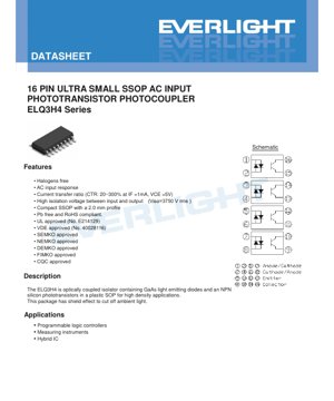
The ELQ3H4 series represents a family of optically coupled isolators designed for high-density applications requiring reliable signal isolation. The core component consists of a Gallium Arsenide (GaAs) light-emitting diode (LED) optically coupled to a silicon NPN phototransistor, all housed within a compact 16-pin Shrink Small Outline Package (SSOP). A key feature of this package is its integrated light shield, which effectively minimizes the impact of ambient light on the phototransistor's performance, enhancing signal integrity in noisy electrical environments.
This device is engineered to accept AC input signals directly, eliminating the need for external rectification circuits in many applications. Its primary value proposition lies in combining a very small form factor (2.0mm profile) with robust isolation performance (3750 Vrms) and compliance with major international safety and environmental standards.
1.1 Core Advantages and Target Market
The ELQ3H4 photocoupler offers several distinct advantages. Its halogen-free construction and compliance with RoHS and Pb-free directives make it suitable for environmentally conscious designs. The device carries approvals from leading safety agencies including UL, VDE, SEMKO, NEMKO, DEMKO, FIMKO, and CQC, facilitating its use in products destined for global markets with stringent regulatory requirements.
The primary target applications are in industrial automation and measurement, where noise immunity and safety are paramount. These include:
- Programmable Logic Controllers (PLCs): For isolating digital I/O signals, communication buses, or analog sensor inputs from the central processing unit.
- Measuring Instruments: Providing isolation in data acquisition systems, multimeters, or oscilloscopes to protect sensitive circuitry from high-voltage test points.
- Hybrid ICs and Power Supplies: Serving as a feedback element in isolated switch-mode power supplies or within custom hybrid modules for gate driving or signal conditioning.
2. In-Depth Technical Parameter Analysis
A thorough understanding of the electrical and optical parameters is crucial for reliable circuit design. The following sections provide a detailed analysis of the key specifications.
2.1 Absolute Maximum Ratings
These ratings define the stress limits beyond which permanent damage to the device may occur. Operation under these conditions is not intended. Key limits for the ELQ3H4 include:
- Input (LED Side): A continuous forward current (IF) of ±60mA and a 1μs pulse current (IFP) of 1A. The power dissipation per channel is 70mW, derating at 0.7mW/°C.
- Output (Phototransistor Side): A collector current (IC) of 50mA. The collector-emitter voltage (VCEO) is 80V, while the emitter-collector voltage (VECO) is a lower 7V, indicating the asymmetry of the phototransistor's breakdown characteristics. Output power dissipation is 150mW per channel, derating at 1.4mW/°C.
- Isolation & Environment: The device withstands an isolation voltage (VISO) of 3750 Vrms for one minute. The operating temperature range is from -55°C to +110°C.
2.2 Electrical and Optical Characteristics
These parameters define the device's performance under normal operating conditions (TA=25°C unless noted).
Input Characteristics: The forward voltage (VF) of the GaAs LED is typically 1.2V at IF = 20mA, with a maximum of 1.4V. The input capacitance (Cin) is up to 250pF, which can affect high-frequency switching performance.
Output Characteristics: The collector-emitter dark current (ICEO) is a maximum of 100nA at VCE=20V with the LED off, representing the phototransistor's leakage. The breakdown voltages (BVCEO=80V, BVECO=7V) confirm the asymmetric structure.
Transfer Characteristics (TA = -40 to 85°C): This is the heart of photocoupler performance.
- Current Transfer Ratio (CTR): Defined as (IC / IF) * 100% at specified conditions. The ELQ3H4 has a very wide CTR range of 20% to 300% at IF = 1mA, VCE = 5V. This wide spread necessitates careful circuit design or binning for precise applications.
- CTR Ratio (CTR1/CTR2): This parameter, ranging from 0.5 to 2.0, indicates the matching between channels in a multi-channel device or the consistency of CTR under AC operation. A ratio of 1.0 represents perfect matching.
- Saturation Voltage: VCE(sat) is typically 0.1V (max 0.2V) at IF=20mA, IC=1mA, indicating good switching characteristics when driven into saturation.
- Isolation Parameters: The isolation resistance (RIO) is a minimum of 5 x 10¹⁰ Ω, and the isolation capacitance (CIO) is typically 0.3pF (max 1.0pF). Low capacitance is critical for rejecting high-frequency common-mode noise.
- Switching Speed: Rise time (tr) and fall time (tf) are specified with a maximum of 18μs each under the test condition of VCE=2V, IC=2mA, RL=100Ω. This indicates the device is suitable for low to medium frequency digital signaling, not high-speed data transmission.
3. Performance Curve Analysis
The datasheet references typical electro-optical characteristic curves. While the specific graphs are not reproduced in the provided text, they typically illustrate the following relationships critical for design:
- CTR vs. Forward Current (IF): Shows how the transfer efficiency changes with LED drive current. CTR often decreases at very high IF due to LED efficiency droop.
- CTR vs. Temperature: Illustrates the temperature dependence of the coupling efficiency, which typically decreases as temperature increases.
- Forward Voltage (VF) vs. Temperature: Shows the negative temperature coefficient of the LED's forward voltage.
- Collector Current (IC) vs. Collector-Emitter Voltage (VCE): The output characteristics of the phototransistor for different input currents, similar to a bipolar transistor's curves.
- Switching Time vs. Load Resistance (RL): Demonstrates how the rise and fall times are affected by the output load. Larger RL generally increases rise time due to increased RC time constant.
Designers should consult the full graphical data to optimize operating points for their specific requirements regarding speed, power consumption, and temperature stability.
4. Mechanical and Package Information
4.1 Package Dimensions and Layout
The ELQ3H4 uses a 16-pin SSOP with a low profile of 2.0mm, enabling high-density PCB mounting. The datasheet includes a detailed dimensioned drawing specifying the package's length, width, height, lead pitch, and lead dimensions. Adherence to these mechanical specifications is essential for proper fit on the PCB and into automated assembly equipment.
A recommended pad layout for surface mount assembly is provided. Following this land pattern is critical to ensure reliable solder joint formation, proper mechanical strength, and to avoid issues like tombstoning during reflow soldering. The pattern accounts for solder fillet formation and thermal relief.
4.2 Device Marking and Polarity
The device is marked on the top of the package. The marking follows the format: EL Q3H4 YWW V.
- EL: Manufacturer identifier.
- Q3H4: Device number.
- Y: One-digit year code.
- WW: Two-digit week code.
- V: Optional marking indicating VDE approval.
Proper orientation is vital. The pin-1 indicator on the package (typically a dot, notch, or beveled edge) must be aligned with the pin-1 marker on the PCB footprint. Incorrect insertion will prevent the device from functioning and may cause damage.
5. Soldering and Assembly Guidelines
5.1 Reflow Soldering Conditions
The device is suitable for surface-mount reflow soldering. The datasheet specifies a critical maximum body temperature profile compliant with IPC/JEDEC J-STD-020D. Key parameters include:
- Preheat: 150°C to 200°C over 60-120 seconds.
- Time Above Liquidus (TL=217°C): 60-100 seconds.
- Peak Temperature (TP): 260°C maximum.
- Time within 5°C of Peak: 30 seconds maximum.
- Maximum Reflow Cycles: 3 times.
Strictly adhering to this profile prevents thermal damage to the plastic package, the internal wire bonds, and the semiconductor die. Exceeding the peak temperature or time-at-temperature can lead to delamination, cracking, or parametric shifts.
5.2 Handling and Storage
Standard ESD (Electrostatic Discharge) precautions must be observed, as the internal GaAs LED and silicon phototransistor are susceptible to damage from static electricity. Use grounded workstations and wrist straps. The devices should be stored in their original moisture-barrier bags with desiccant in a controlled environment (typically <40°C/90% RH) to prevent moisture absorption, which can cause \"popcorning\" during reflow.
6. Packaging and Ordering Information
6.1 Model Numbering and Options
The part number structure is: ELQ3H4(Z)-V.
- Z (Packing Option): \"TA\" denotes Tape and Reel packaging. If omitted, the default is Tube packaging.
- V (Approval Option): Denotes VDE approval marking.
Packing Quantities: Tube option contains 40 units per tube. The Tape and Reel (TA) option contains 1000 units per reel.
6.2 Tape and Reel Specifications
Detailed dimensions for the carrier tape are provided, including pocket size (A0, B0, D0, D1), pitch (P0), and reel dimensions. This information is necessary for configuring automated pick-and-place machines correctly. The tape width (W) is 16.0mm ± 0.3mm, and the feed direction is specified.
7. Application Design Considerations
7.1 Input Circuit Design
For AC input operation, the LED can be driven directly by an AC signal. A current-limiting resistor is mandatory to set the desired forward current (IF). Its value must be calculated based on the peak voltage of the AC signal, the LED's VF, and the desired IF. Since the LED is a diode, it will only conduct during half-cycles unless a bridge rectifier is used in front of it for full-wave operation. The wide CTR range means the output current will vary significantly between devices if a fixed IF is used. For more consistent performance, consider using a higher IF (where CTR variation might be lower) or implementing feedback.
3.2 Output Circuit Design
The phototransistor can be used in either a switch or linear mode. For digital switching, the device is driven into saturation (IF high enough to make VCE ≈ VCE(sat)). The load resistor (RL) connected to the collector determines the output voltage swing and affects switching speed (larger RL increases rise time). For analog or linear applications, the phototransistor operates in its active region. However, the nonlinearity of the CTR vs. IF curve and its strong temperature dependence make precise linear operation challenging without compensation.
7.3 Noise Immunity and Layout
To maximize the high isolation capability (3750Vrms, low CIO), careful PCB layout is essential. Maintain adequate creepage and clearance distances between the input and output sides of the circuit as per safety standards. Use a ground plane, but consider splitting the plane under the photocoupler to minimize capacitive coupling across the isolation barrier. Bypass capacitors placed close to the device pins on both sides can help suppress high-frequency noise.
8. Technical Comparison and Selection Guidance
The ELQ3H4's key differentiators are its AC input capability, ultra-small SSOP package, and comprehensive safety certifications. When selecting a photocoupler, compare the following against project requirements:
- vs. DC-Input Photocouplers: The ELQ3H4 simplifies circuits by eliminating external rectifiers for AC signals, saving board space and cost.
- vs. Larger Packages (DIP, etc.): The SSOP offers significant space savings but may have slightly different thermal characteristics and requires more precise assembly.
- vs. High-Speed Optocouplers: Devices with faster logic gates or digital isolators offer much higher data rates (>1 Mbps) but may have different isolation ratings, power requirements, or cost structures.
- vs. Photocouplers with Darlington Output: Darlington configurations offer much higher CTR (500-1000%) but have slower switching speeds and higher saturation voltages.
- CTR Bin Selection: If circuit performance is highly sensitive to gain, inquire about availability of devices binned into narrower CTR ranges (e.g., 100-200%).
9. Frequently Asked Questions (FAQ)
Q1: Can I drive the LED with a voltage source directly?
A1: No. An LED is a current-driven device. Always use a series current-limiting resistor to control IF and prevent damage from overcurrent.
Q2: Why is the output rise time slower than the fall time in the specifications?
A2: This is typical for phototransistors. The rise time is limited by the time required to charge the phototransistor's junction capacitance through the photocurrent. The fall time is governed by the discharge of this capacitance through the external load resistor and the device's internal recombination processes.
Q3: How does temperature affect performance?
A3: CTR generally decreases with increasing temperature. The LED's forward voltage (VF) also decreases. These effects must be accounted for in designs operating over a wide temperature range to ensure reliable switching thresholds or linearity.
Q4: What is the purpose of the \"shield effect\" mentioned?
A4: The opaque plastic package acts as a light shield, blocking ambient light from reaching the phototransistor. This prevents false triggering or offset currents caused by external light sources like room lighting or sunlight.
10. Practical Application Example
Scenario: Isolated AC Mains Detection for a PLC Input Module.
A common use case is detecting the presence of a 120V AC signal from a switch or sensor. The ELQ3H4 is ideal for this.
- Input Circuit: The 120V AC signal is stepped down via a high-value, high-voltage resistor network to limit the current. A reverse-parallel protection diode may be placed across the LED to clamp reverse voltage during the negative half-cycle, although the device is rated for AC operation. The resistor value is chosen to set IF to a nominal 5-10mA, well within the ratings.
- Output Circuit: The phototransistor collector is connected to the PLC's logic supply voltage (e.g., 3.3V or 5V) through a pull-up resistor (RL). The emitter is grounded. When AC is present, the phototransistor turns on during the conducting half-cycles, pulling the collector output low. The PLC's digital input reads this pulsating low signal. Software can then debounce or detect the zero-crossings to confirm AC presence.
- Benefits: This design provides robust galvanic isolation, protecting the sensitive PLC circuitry from mains transients and faults. The compact SSOP package allows many such channels to be placed on a single module.
11. Operating Principle
A photocoupler operates on the principle of optical coupling to achieve electrical isolation. An electrical input signal drives a light-emitting diode (LED), causing it to emit infrared light proportional to the current. This light travels across a short, transparent gap within the package and strikes the base region of a silicon phototransistor. The incident photons generate electron-hole pairs in the base, effectively acting as a base current. This photogenerated current is then amplified by the transistor's gain, producing a collector current that is an electrical replica of the input signal. The key is that the signal transfer occurs through light, with no electrical connection between the input and output, creating the isolation barrier.
12. Technology Trends
The field of signal isolation continues to evolve. While traditional phototransistor-based couplers like the ELQ3H4 remain dominant for cost-effective, medium-speed, and high-isolation applications, several trends are notable:
- Increased Integration: Multi-channel photocouplers in single packages are common, reducing board space and cost per channel.
- Higher Speed Alternatives: For data communication, digital isolators based on CMOS technology and RF or capacitive coupling offer significantly higher data rates (up to hundreds of Mbps), lower power consumption, and better timing consistency, though often at different isolation voltage ratings.
- Enhanced Reliability and Certification: There is a continuous push for higher reliability metrics (FIT rates), wider operating temperature ranges, and obtaining certifications for emerging standards, particularly in automotive (AEC-Q100) and medical applications.
- Package Miniaturization: The drive for smaller, thinner packages continues to enable more compact end products, as seen with the 2.0mm profile SSOP used in the ELQ3H4.
LED Specification Terminology
Complete explanation of LED technical terms
Photoelectric Performance
| Term | Unit/Representation | Simple Explanation | Why Important |
|---|---|---|---|
| Luminous Efficacy | lm/W (lumens per watt) | Light output per watt of electricity, higher means more energy efficient. | Directly determines energy efficiency grade and electricity cost. |
| Luminous Flux | lm (lumens) | Total light emitted by source, commonly called "brightness". | Determines if the light is bright enough. |
| Viewing Angle | ° (degrees), e.g., 120° | Angle where light intensity drops to half, determines beam width. | Affects illumination range and uniformity. |
| CCT (Color Temperature) | K (Kelvin), e.g., 2700K/6500K | Warmth/coolness of light, lower values yellowish/warm, higher whitish/cool. | Determines lighting atmosphere and suitable scenarios. |
| CRI / Ra | Unitless, 0–100 | Ability to render object colors accurately, Ra≥80 is good. | Affects color authenticity, used in high-demand places like malls, museums. |
| SDCM | MacAdam ellipse steps, e.g., "5-step" | Color consistency metric, smaller steps mean more consistent color. | Ensures uniform color across same batch of LEDs. |
| Dominant Wavelength | nm (nanometers), e.g., 620nm (red) | Wavelength corresponding to color of colored LEDs. | Determines hue of red, yellow, green monochrome LEDs. |
| Spectral Distribution | Wavelength vs intensity curve | Shows intensity distribution across wavelengths. | Affects color rendering and quality. |
Electrical Parameters
| Term | Symbol | Simple Explanation | Design Considerations |
|---|---|---|---|
| Forward Voltage | Vf | Minimum voltage to turn on LED, like "starting threshold". | Driver voltage must be ≥Vf, voltages add up for series LEDs. |
| Forward Current | If | Current value for normal LED operation. | Usually constant current drive, current determines brightness & lifespan. |
| Max Pulse Current | Ifp | Peak current tolerable for short periods, used for dimming or flashing. | Pulse width & duty cycle must be strictly controlled to avoid damage. |
| Reverse Voltage | Vr | Max reverse voltage LED can withstand, beyond may cause breakdown. | Circuit must prevent reverse connection or voltage spikes. |
| Thermal Resistance | Rth (°C/W) | Resistance to heat transfer from chip to solder, lower is better. | High thermal resistance requires stronger heat dissipation. |
| ESD Immunity | V (HBM), e.g., 1000V | Ability to withstand electrostatic discharge, higher means less vulnerable. | Anti-static measures needed in production, especially for sensitive LEDs. |
Thermal Management & Reliability
| Term | Key Metric | Simple Explanation | Impact |
|---|---|---|---|
| Junction Temperature | Tj (°C) | Actual operating temperature inside LED chip. | Every 10°C reduction may double lifespan; too high causes light decay, color shift. |
| Lumen Depreciation | L70 / L80 (hours) | Time for brightness to drop to 70% or 80% of initial. | Directly defines LED "service life". |
| Lumen Maintenance | % (e.g., 70%) | Percentage of brightness retained after time. | Indicates brightness retention over long-term use. |
| Color Shift | Δu′v′ or MacAdam ellipse | Degree of color change during use. | Affects color consistency in lighting scenes. |
| Thermal Aging | Material degradation | Deterioration due to long-term high temperature. | May cause brightness drop, color change, or open-circuit failure. |
Packaging & Materials
| Term | Common Types | Simple Explanation | Features & Applications |
|---|---|---|---|
| Package Type | EMC, PPA, Ceramic | Housing material protecting chip, providing optical/thermal interface. | EMC: good heat resistance, low cost; Ceramic: better heat dissipation, longer life. |
| Chip Structure | Front, Flip Chip | Chip electrode arrangement. | Flip chip: better heat dissipation, higher efficacy, for high-power. |
| Phosphor Coating | YAG, Silicate, Nitride | Covers blue chip, converts some to yellow/red, mixes to white. | Different phosphors affect efficacy, CCT, and CRI. |
| Lens/Optics | Flat, Microlens, TIR | Optical structure on surface controlling light distribution. | Determines viewing angle and light distribution curve. |
Quality Control & Binning
| Term | Binning Content | Simple Explanation | Purpose |
|---|---|---|---|
| Luminous Flux Bin | Code e.g., 2G, 2H | Grouped by brightness, each group has min/max lumen values. | Ensures uniform brightness in same batch. |
| Voltage Bin | Code e.g., 6W, 6X | Grouped by forward voltage range. | Facilitates driver matching, improves system efficiency. |
| Color Bin | 5-step MacAdam ellipse | Grouped by color coordinates, ensuring tight range. | Guarantees color consistency, avoids uneven color within fixture. |
| CCT Bin | 2700K, 3000K etc. | Grouped by CCT, each has corresponding coordinate range. | Meets different scene CCT requirements. |
Testing & Certification
| Term | Standard/Test | Simple Explanation | Significance |
|---|---|---|---|
| LM-80 | Lumen maintenance test | Long-term lighting at constant temperature, recording brightness decay. | Used to estimate LED life (with TM-21). |
| TM-21 | Life estimation standard | Estimates life under actual conditions based on LM-80 data. | Provides scientific life prediction. |
| IESNA | Illuminating Engineering Society | Covers optical, electrical, thermal test methods. | Industry-recognized test basis. |
| RoHS / REACH | Environmental certification | Ensures no harmful substances (lead, mercury). | Market access requirement internationally. |
| ENERGY STAR / DLC | Energy efficiency certification | Energy efficiency and performance certification for lighting. | Used in government procurement, subsidy programs, enhances competitiveness. |